
A Thin-Film Pinned-Photodiode Imager Pixel with Fully Monolithic Fabrication and beyond 1Me- Full Well Capacity

 , , , , , , ,
  , add
Show full author list
, add
Show full author list
Abstract
:1. Introduction
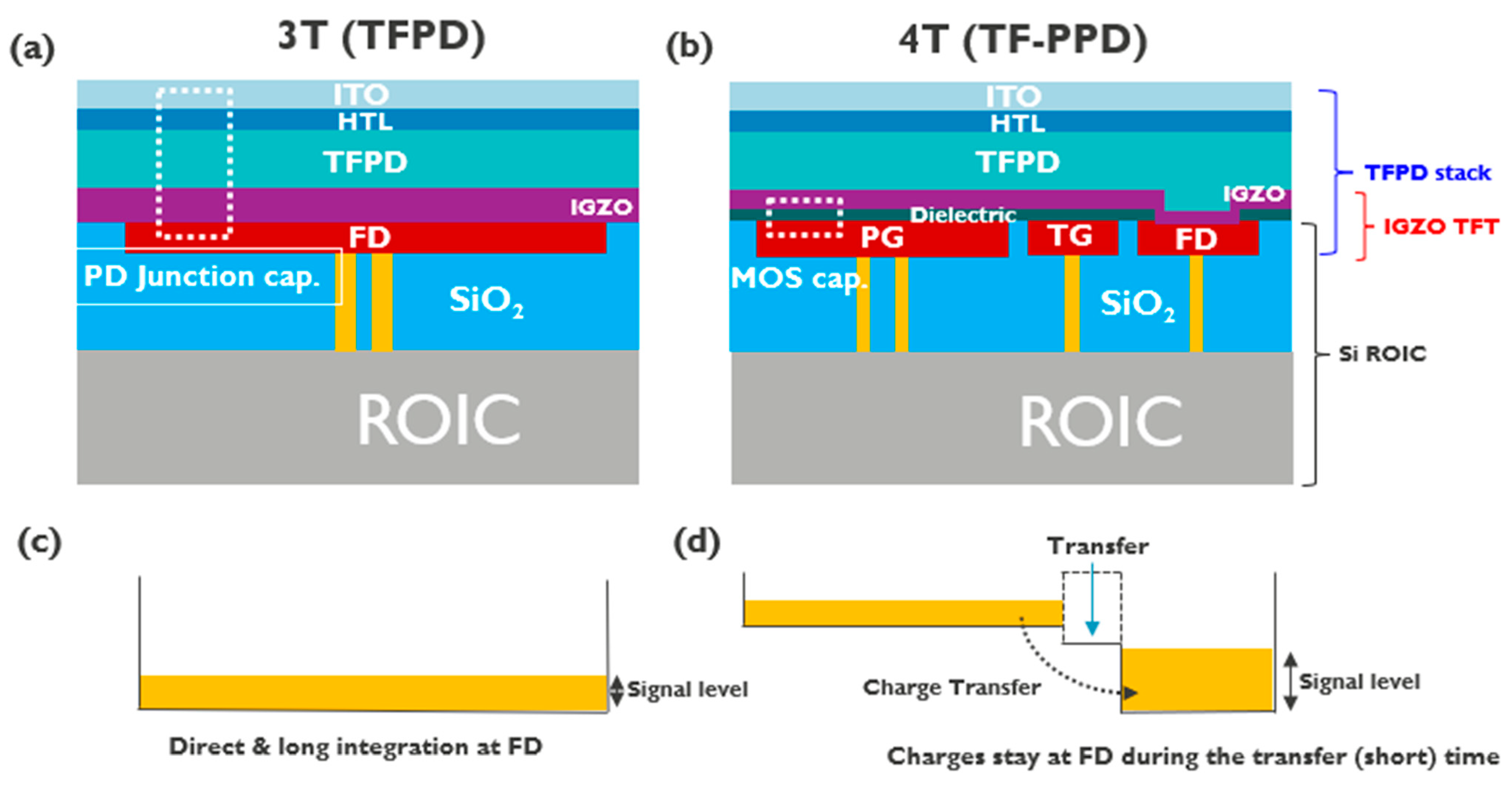
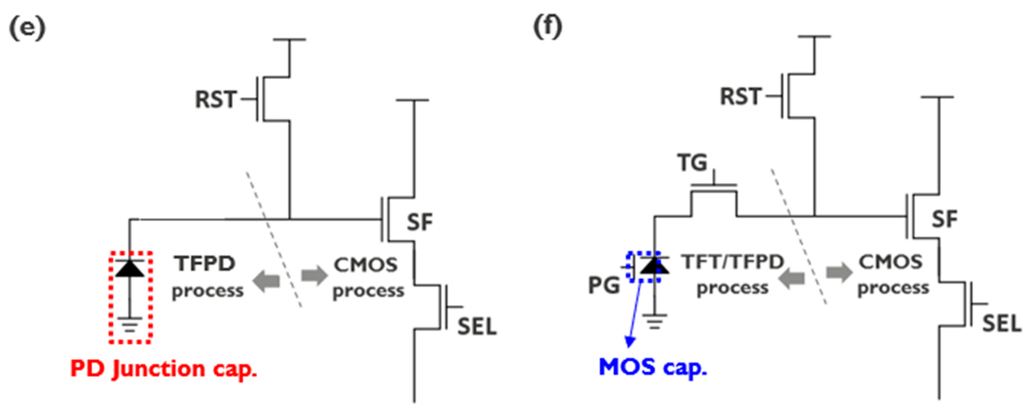
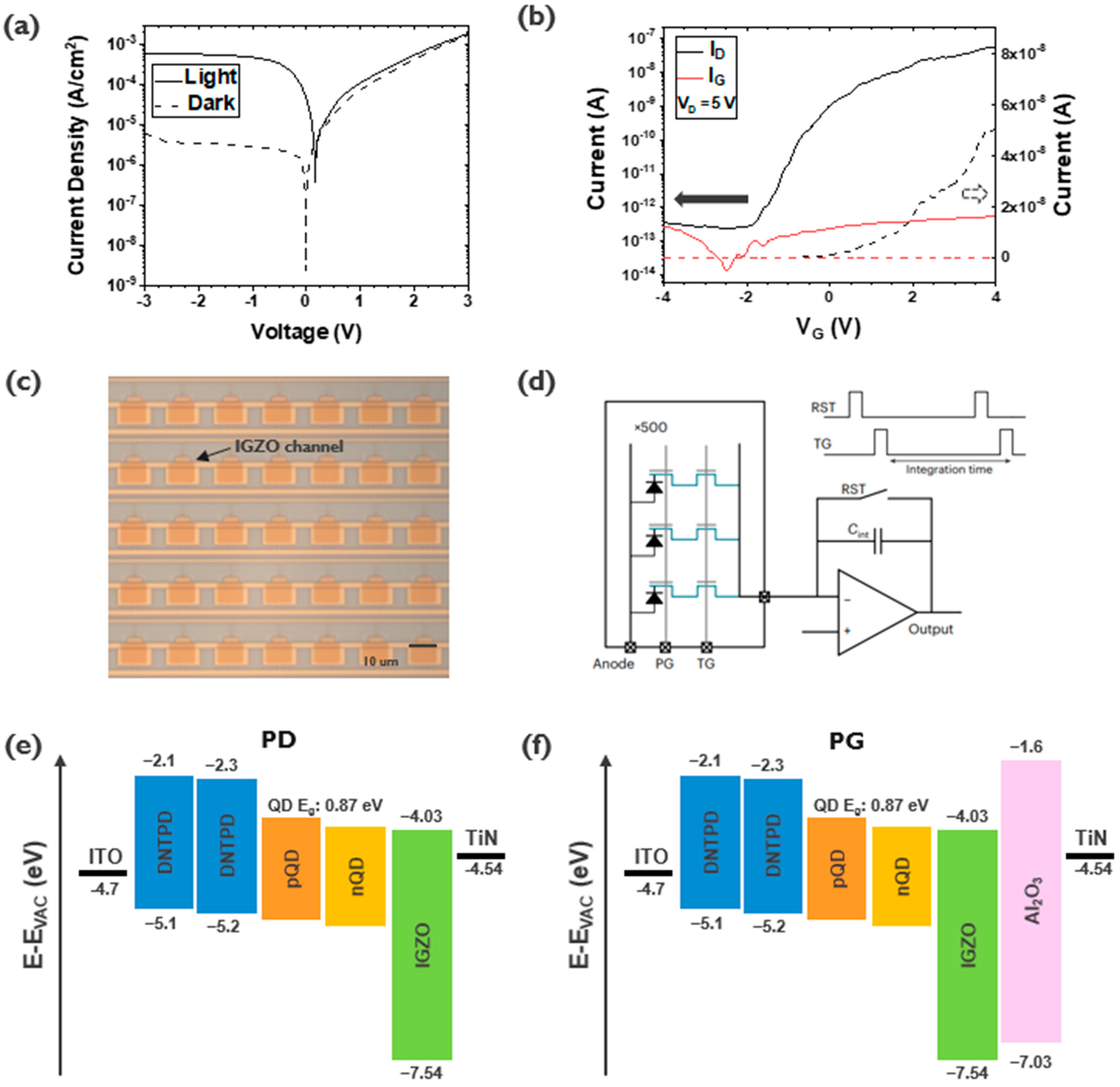
2. Device Configuration and Measurements
3. Simulation and Experimental Results
3.1. TCAD Simulations
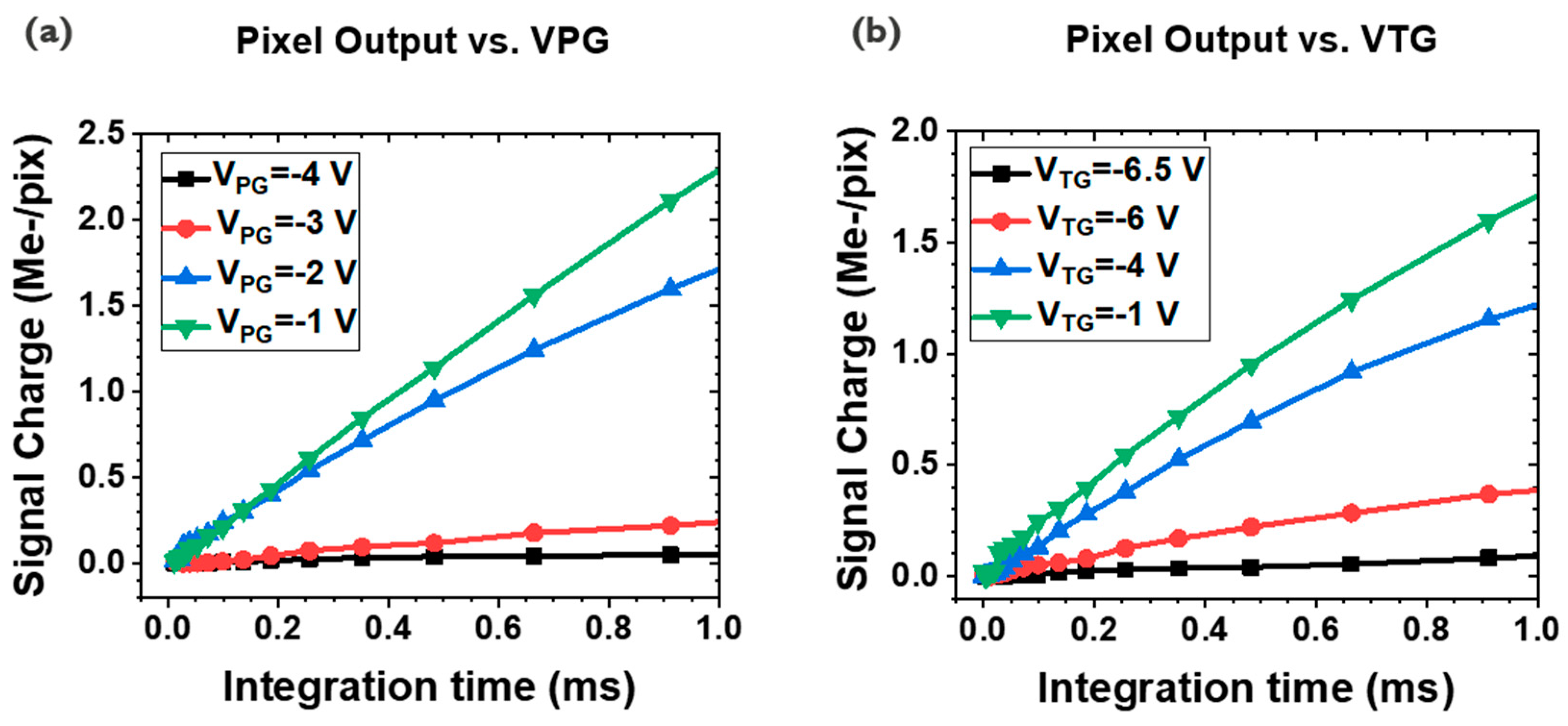
3.2. Pixel Output Responses by the PG and TG Bias Sweep
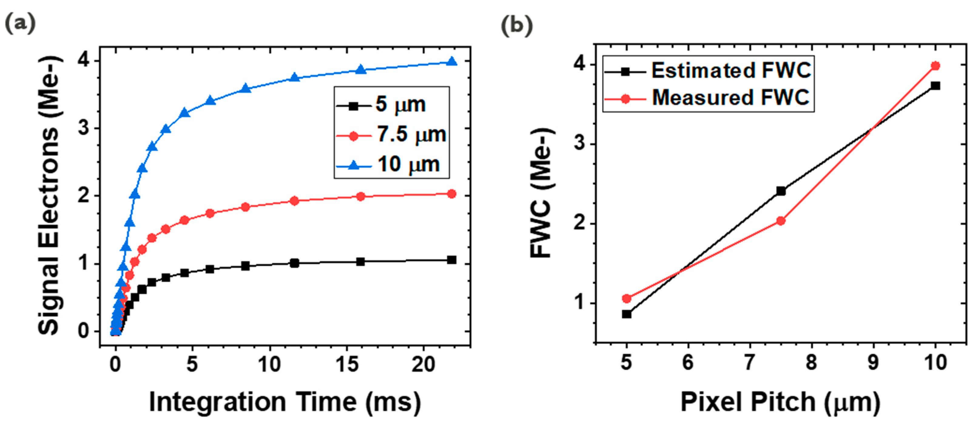
3.3. Full-Well Capacity (FWC)
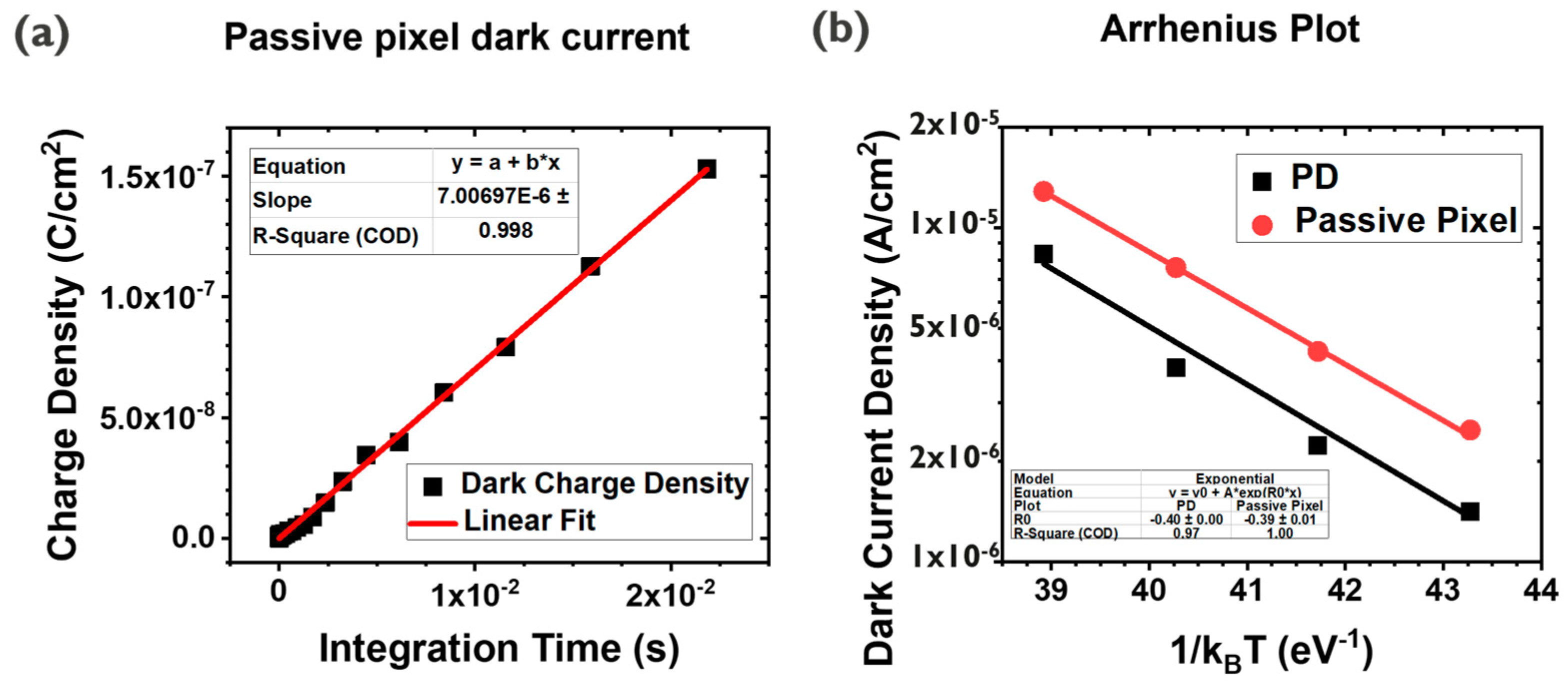
3.4. Dark Current
4. Discussion
5. Conclusions
Author Contributions
Funding
Institutional Review Board Statement
Informed Consent Statement
Data Availability Statement
Acknowledgments
Conflicts of Interest
References
- Takase, M.; Miyake, Y.; Yamada, T.; Tamaki, T.; Murakami, M.; Inoue, Y. First demonstration of 0.9 μm pixel global shutter operation by novel charge control in organic photoconductive film. In Proceedings of the 2015 IEEE International Electron Devices Meeting (IEDM), Washington, DC, USA, 7–9 December 2015; pp. 30.2.1–30.2.4. [Google Scholar]
- Malinowski, P.E.; Pejović, V.; Lieberman, I.; Kim, J.J.; Siddik, A.B.; Georgitzikis, E.; Lim, M.J.; Hagelsieb, L.M.; Hermans, Y.; Monroy, I.P.; et al. Image sensors using thin-film absorbers. Appl. Opt. 2023, 62, F21–F30. [Google Scholar] [CrossRef] [PubMed]
- Malinowski, P.E.; Pejović, V.; Georgitzikis, E.; Kim, J.H.; Lieberman, I.; Papadopoulos, N.; Lim, M.J.; Hagelsieb, L.M.; Chandrasekaran, N.; Puybaret, R.; et al. Colloidal quantum dot image sensors: A new vision for infrared. In Proceedings of the 2022 International Electron Devices Meeting (IEDM), San Francisco, CA, USA, 3–7 December 2022; pp. 19.3.1–19.3.4. [Google Scholar]
- Pejović, V.; Georgitzikis, E.; Lee, J.; Lieberman, I.; Cheyns, D.; Heremans., P.; Malinowski, P.E. Infrared colloidal quantum dot image sensors. IEEE Trans. Electron Devices 2022, 69, 2840–2850. [Google Scholar] [CrossRef]
- Lee, J.; Georgitzikis, E.; Li, Y.; Lin, Z.; Park, J.; Lieberman, I.; Cheyns, D.; Jayapala1, M.; Lambrechts, A.; Thijs, S.; et al. Imaging in short-wave infrared with 1.82 μm pixel quantum dot image sensor. In Proceedings of the 2020 IEEE International Electron Devices Meeting (IEDM), San Francisco, CA, USA, 12–18 December 2020; pp. 16.5.1–16.5.4. [Google Scholar]
- Steckel, J.S.; Josse, E.; Pattantyus-Abraham, A.G.; Bidaud, M.; Mortini, B.; Bilgen, H.; Arnaud, O.; Allegret-Maret, S.; Saguin, F.; Mazet, L.; et al. 1.62 µm global shutter quantum dot image sensor optimized for near and shortwave infrared. In Proceedings of the 2021 IEEE International Electron Devices Meeting (IEDM), San Francisco, CA, USA, 11–16 December 2021; pp. 23.4.1–23.4.4. [Google Scholar]
- Sim, K.M.; Yoon, S.; Cho, J.; Jang, M.S.; Chung, D.S. Facile tuning the detection spectrum of organic thin film photodiode via selective exciton activation. ACS Appl. Mater. Interfaces 2018, 10, 8405–8410. [Google Scholar] [CrossRef] [PubMed]
- Teranishi, N.; Kohono, A.; Ishihara, Y.; Oda, E.; Arai, K. No image lag photodiode structure in the interline CCD image sensor. In Proceedings of the 1982 International Electron Devices Meeting, San Francisco, CA, USA, 13–15 December 1982; pp. 324–327. [Google Scholar]
- Fossum, E.R. Active pixel sensors: Are CCDs dinosaurs? In Proceedings of the IS&T/SPIE’s Symposium on Electronic Imaging: Science and Technology, San Jose, CA, USA, 12 July 1993; Volume 1900, pp. 2–14. [Google Scholar]
- Fossum, E.R.; Hondongwa, D.B. A review of the pinned photodiode for CCD and CMOS image sensors. Dartm. Scholarsh. 2014, 2423, 33–43. [Google Scholar] [CrossRef]
- Lee, J.; Georgitzikis, E.; Hermans, Y.; Papadopoulos, N.; Chandrasekaran, N.; Jin, M.; Siddik, A.B.; Roose, F.D.; Uytterhoeven, G.; Kim, J.H.; et al. Thin-film image sensors with a pinned photodiode structure. Nat. Electron. 2023, 6, 590–598. [Google Scholar] [CrossRef]
- Matsuo, T.; Mori, S.; Ban, A.; Imaya, A. Advantages of IGZO oxide semiconductor. In Proceedings of the SID Symposium Digest of Technical Papers, San Diego, CA, USA, 1–6 June 2014; Volume 45, pp. 83–86. [Google Scholar]
- Yu, E.K.; Jun, S.; Kim, D.H.; Kanicki, J. Density of states of amorphous In-Ga-Zn-O from electrical and optical characterization. J. Appl. Phys. 2014, 116, 154505. [Google Scholar] [CrossRef]
- Seo, M.; Chu, M.; Jung, H.; Kim, S.; Song, J.; Bae, D.; Lee, S.; Lee, J.; Kim, S.; Lee, J.; et al. 2.45 e-RMS low-random-noise, 598.5 mW low-power, and 1.2 kfps high-speed 2-Mp global shutter CMOS image sensor with pixel-level ADC and memory. IEEE J. Solid-State Circuits 2022, 57, 1125–1137. [Google Scholar] [CrossRef]
- Janbu, Ø.; Johansson, R.; Martinussen, T.; Solhusvik, J. A 1.17-megapixel CMOS image sensor with 1.5 A/D conversions per digital CDS pixel readout and four in-pixel gain steps. IEEE J. Solid-State Circuits 2019, 54, 2568–2578. [Google Scholar] [CrossRef]
- Kalyanam, P.; Chapman, G.H.; Parameswaran, A.M. Simulating enhanced photo carrier collection in the multifinger photogate active pixel sensors. In Proceedings of the Sensors, Cameras, and Systems for Industrial, Scientific, and Consumer Applications XII, San Francisco, CA, USA, 25–27 January 2011. [Google Scholar]
- Tanner, C.M.; Perng, Y.; Frewin, C.; Saddow, S.E.; Chang, J.P. Electrical performance of gate dielectric films deposited by atomic layer deposition on 4H-SiC. Appl. Phys. Lett. 2007, 91, 203510. [Google Scholar] [CrossRef]
- Wilk, G.D.; Wallace, R.M.; Anthony, J.M. High-κ gate dielectrics: Current status and materials properties considerations. J. Appl. Phys. 2001, 89, 5243–5275. [Google Scholar] [CrossRef]
- Vitale, S.A.; Kedzierski, J.; Healey, P.; Wyatt, P.W.; Keast, C.L. Work-function-tuned TiN metal gate FDSOI transistors for subthreshold operation. IEEE Trans. Electron Devices 2011, 58, 419–426. [Google Scholar] [CrossRef]
- Siddik, A.B.; Georgitzikis, E.; Hermans, Y.; Kang, J.; Kim, J.H.; Pejovic, V.; Lieberman, I.; Malinowski, P.E.; Kadashchuk, A.; Genoe, J.; et al. Interface-engineered organic near-infrared photodetector for imaging applications. ACS Appl. Mater. Interfaces 2023, 15, 30534–30542. [Google Scholar] [CrossRef] [PubMed]
- Kim, J.H.; Pejović, V.; Georgitzikis, E.; Li, Y.; Kim, J.; Malinowski, P.E.; Lieberman, I.; Cheyns, D.; Heremans, P.; Lee, J. Detailed characterization of short-wave infrared colloidal quantum dot image sensors. IEEE Trans. Electron Devices 2022, 69, 2900–2906. [Google Scholar] [CrossRef]
- Murata, M.; Kuroda, R.; Fujihara, Y.; Aoyagi, Y.; Shibata, H.; Shibaguchi, T.; Kamata, Y.; Miura, N.; Kuriyama, N. A 24.3Me− full well capacity CMOS image sensor with lateral overflow integration trench capacitor for high precision near infrared absorption imaging. In Proceedings of the 2018 IEEE International Electron Devices Meeting (IEDM), San Francisco, CA, USA, 1–5 December 2018; pp. 10.3.1–10.3.4. [Google Scholar]
- Lalanne, F.; Malinge, P.; Hérault, D.; Jamin-Mornet, C.; Virollet, N. A 750 K Photocharge linear full well in a 3.2 µm HDR pixel with complementary carrier collection. Sensors 2018, 18, 305. [Google Scholar] [CrossRef] [PubMed]
- Kim, W.; Park, C.; Lee, H.; Lee, I.; Lee, B. A high full well capacity CMOS image sensor for space applications. Sensors 2019, 19, 1505. [Google Scholar] [CrossRef] [PubMed]
- Zaitsu, K.; Matsumoto, A.; Nishida, M.; Tanaka, Y.; Yamashita, H.; Satake, Y.; Watanabe, T.; Araki, K.; Nei, N.; Nakazawa, K.; et al. A 2-layer transistor pixel stacked CMOS image sensor with oxide-based full trench isolation for large full well capacity and high quantum efficiency. In Proceedings of the 2022 IEEE Symposium on VLSI Technology and Circuits (VLSI Technology and Circuits), Honolulu, HI, USA, 12–17 June 2022; pp. 286–287. [Google Scholar]
- Kwon, Y.; Seo, S.; Cho, S.; Choi, S.; Hwang, T.; Kim, Y.; Jin, Y.; Oh, Y.; Keel, M.; Kim, D.; et al. A 2.8 μm pixel for time of flight CMOS image sensor with 20 ke- full-well capacity in a tap and 36% quantum efficiency at 940 nm wavelength. In Proceedings of the 2020 IEEE International Electron Devices Meeting (IEDM), San Francisco, CA, USA, 12–18 December 2020; pp. 33.2.1–33.2.4. [Google Scholar]
- Yun, J.; Lee, S.; Cha, S.; Kim, J.; Lee, J.; Kim, H.; Lee, E.; Kim, S.; Hong, S.; Kim, H.; et al. A 0.6 μm small pixel for high resolution CMOS image sensor with full well capacity of 10,000e- by dual vertical transfer gate technology. In Proceedings of the 2022 IEEE Symposium on VLSI Technology and Circuits (VLSI Technology and Circuits), Honolulu, HI, USA, 12–17 June 2022; pp. 351–352. [Google Scholar]
- Brunetti, A.M.; Musolino, M.; Choubey, B. Staggered pixel layout to reduce area and increase full well capacity in CMOS image sensors. IEEE Trans. Electron Devices 2021, 68, 572–577. [Google Scholar] [CrossRef]
- Takayanagi, I.; Miyauchi, K.; Okura, S.; Mori, K.; Nakamura, J.; Sugawa, S. A 120-ke- full-well capacity 160-µV/e- conversion gain 2.8-µm backside-illuminated pixel with a lateral overflow integration capacitor. Sensors 2019, 19, 5572. [Google Scholar] [CrossRef] [PubMed]
- Kim, H.; Kim, Y.H.; Moon, S.; Kim, H.; Yoo, B.; Park, J.; Kim, S.; Koo, J.; Seo, S.; Shin, H.J.; et al. A 0.64 μm 4-photodiode 1.28 μm 50Mpixel CMOS image sensor with 0.98e- temporal noise and 20Ke- full-well capacity employing quarter-ring source-follower. In Proceedings of the 2023 IEEE International Solid-State Circuits Conference (ISSCC), San Francisco, CA, USA, 19–23 February 2023; pp. 1–3. [Google Scholar]
- Wakashima, S.; Kusuhara, F.; Kuroda, R.; Sugawa, S. A linear response single exposure CMOS image sensor with 0.5e− readout noise and 76ke− full well capacity. In Proceedings of the 2015 Symposium on VLSI Circuits (VLSI Circuits), Kyoto, Japan, 17–19 June 2015; pp. C88–C89. [Google Scholar]
- Venezia, V.C.; Hsiung, A.C.; Ai, K.; Zhao, X.; Lin, Z.; Mao, D.; Yazdani, A.; Webster, E.A.G.; Grant, L.A. 1.5µm dual conversion gain, backside illuminated image sensor using stacked pixel level connections with 13ke-full-well capacitance and 0.8e-noise. In Proceedings of the 2018 IEEE International Electron Devices Meeting (IEDM), San Francisco, CA, USA, 1–5 December 2018; pp. 10.1.1–10.1.4. [Google Scholar]
- Sakai, S.; Tashiro, Y.; Kuroda, R.; Sugawa, S. A 2.8 µm pixel-pitch 55 ke- full-well capacity global-shutter complementary metal oxide semiconductor image sensor using lateral overflow integration capacitor. Jpn. J. Appl. Phys. 2013, 52, 04CE01. [Google Scholar] [CrossRef]
- Kumagai, Y.; Yoshita, R.; Osawa, N.; Ikeda, H.; Yamashita, K.; Abe, T.; Kudo, S.; Yamane, J.; Idekoba, T.; Noudo, S.; et al. Back-illuminated 2.74 µm-pixel-pitch global shutter CMOS image sensor with charge-domain memory achieving 10k e- saturation signal. In Proceedings of the 2018 IEEE International Electron Devices Meeting (IEDM), San Francisco, CA, USA, 1–5 December 2018; pp. 10.6.1–10.6.4. [Google Scholar]
- Sawai, Y.; Isozaki, T.; Yasuda, N.; Miyauchi, K.; Fu, K.; Mori, K. A 5.6 µm stacked voltage domain global shutter pixel with 88ke- linear full well capacity and 85dB single exposure high dynamic range. In Proceedings of the 2021 International Image Sensor Workshop (IISW), Online, 20–23 September 2021. R51. [Google Scholar]
- Choi, S.; Lim, S.; Lim, M.; Bae, H.J.; Choo, K.J.; Park, J.H.; Lee, K.S.; Kim, S.S.; Moon, S.; Son, K.; et al. Back-side illuminated 28M-pixel APS-C sensor with high performance. In Proceedings of the 2015 International Image Sensor Workshop (IISW), Vaals, The Netherlands, 8–11 June 2015. 1-02. [Google Scholar]
- Lee, J.; Kim, S.S.; Baek, I.; Shim, H.; Kim, T.; Kim, T.; Kyoung, J.; Im, D.; Choi, J.; Cho, K.Y.; et al. A 2.1e− temporal noise and −105dB parasitic light sensitivity backside-illuminated 2.3 µm-pixel voltage-domain global shutter CMOS image sensor using high-capacity DRAM capacitor technology. In Proceedings of the 2020 IEEE International Solid-State Circuits Conference—(ISSCC), San Francisco, CA, USA, 16–20 February 2020; pp. 102–104. [Google Scholar]
- Takayanagi, I.; Yoshimura, N.; Mori, K.; Matsuo, S.; Tanaka, S.; Abe, H.; Yasuda, N.; Ishikawa, K.; Okura, S.; Ohsawa, S.; et al. An over 90 dB intra-scene single-exposure dynamic range CMOS image sensor using a 3.0 µm triple-gain pixel fabricated in a standard BSI process. Sensors 2018, 18, 203. [Google Scholar] [CrossRef] [PubMed]
- Uchida, T.; Yamashita, K.; Masagaki, A.; Kawamura, T.; Tokumitsu, C.; Iwabuchi, S.; Onizawa, T.; Ohura, M.; Ansai, H.; Izukashi, K.; et al. A 2.9 µm pixel CMOS image sensor for security cameras with high FWC and 97 dB single-exposure dynamic range. In Proceedings of the 2021 IEEE International Electron Devices Meeting (IEDM), San Francisco, CA, USA, 11–15 December 2021; pp. 30.3.1–30.3.4. [Google Scholar]
- Oh, Y.; Lim, J.; Park, S.; Yoo, D.; Lim, M.; Park, J.; Kim, S.; Jung, M.; Kim, S.; Lee, J.; et al. A 140 dB single-exposure dynamic-range CMOS image sensor with in-Pixel DRAM capacitor. In Proceedings of the 2022 International Electron Devices Meeting (IEDM), San Francisco, CA, USA, 3–7 December 2022; pp. 37.7.1–37.7.4. [Google Scholar]
- Innocent, M.; Velichko, S.; Lloyd, D.; Beck, J.; Hernandez, A.; Vanhoff, B.; Silsby, C.; Oberoi, A.; Singh, G.; Gurindagunta, S.; et al. Automotive 8.3 MP CMOS image sensor with 150 dB dynamic range and light flicker mitigation. In Proceedings of the 2021 IEEE International Electron Devices Meeting (IEDM), San Francisco, CA, USA, 11–15 December 2021; pp. 30.2.1–30.2.4. [Google Scholar]
- Sakano, Y.; Toyoshima, T.; Nakamura, R.; Asatsuma, T.; Hattori, Y.; Yamanaka, T.; Yoshikawa, R.; Kawazu, N.; Matsuura, T.; Iinuma, T.; et al. A 132dB single-exposure-dynamic-range CMOS image sensor with high temperature tolerance. In Proceedings of the 2020 IEEE International Solid- State Circuits Conference—(ISSCC), San Francisco, CA, USA, 16–20 February 2020; pp. 106–108. [Google Scholar]
- Funatsu, R.; Huang, S.; Yamashita, T.; Stevulak, K.; Rysinski, J.; Estrada, D.; Yan, S.; Soeno, T.; Nakamura, T.; Hayashida, T.; et al. 133Mpixel 60fps CMOS image sensor with 32-column shared high-speed column-parallel SAR ADCs. In Proceedings of the 2015 IEEE International Solid-State Circuits Conference—(ISSCC) Digest of Technical Papers, San Francisco, CA, USA, 22–26 February 2015; pp. 1–3. [Google Scholar]
- Takase, M.; Isono, S.; Tomekawa, Y.; Koyanagi, T.; Tokuhara, T.; Harada, M.; Inoue, Y. An over 120 dB wide-dynamic-range 3.0 μm pixel image sensor with in-pixel capacitor of 41.7 fF/um2 and high reliability enabled by BEOL 3D capacitor process. In Proceedings of the 2018 IEEE Symposium on VLSI Technology, Honolulu, HI, USA, 18–22 June 2018; pp. 71–72. [Google Scholar]
- Stark, L.; Raynor, J.M.; Lalanne, F.; Henderson, R.K. Back-illuminated voltage-domain global shutter CMOS image sensor with 3.75 µm pixels and dual in-pixel storage nodes. In Proceedings of the 2016 IEEE Symposium on VLSI Technology, Honolulu, HI, USA, 14–16 June 2016; pp. 1–2. [Google Scholar]
- Nishimura, K.; Sato, Y.; Hirase, J.; Sakaida, R.; Yanagida, M.; Tamaki, T.; Takase, M.; Kanehara, H.; Murakami, M.; Inoue, Y. An over 120dB simultaneous-capture wide-dynamic-range 1.6e− ultra-low-reset-noise organic-photoconductive-film CMOS image sensor. In Proceedings of the 2016 IEEE International Solid-State Circuits Conference (ISSCC), San Francisco, CA, USA, 31 January–4 February 2016; pp. 110–111. [Google Scholar]


| Pixel Pitch | Fill Factor | Estimated FWC | Measured FWC |
|---|---|---|---|
| 5 μm | 46% | 0.9 Me- | 1.1 Me- |
| 73% | 1.4 Me- | 1.4 Me- | |
| 7.5 μm | 57% | 2.4 Me- | 2.0 Me- |
| 88% | 3.7 Me- | 4.2 Me- | |
| 10 μm | 50% | 3.7 Me- | 4.0 Me- |
| 81% | 6.1 Me- | 5.6 Me- |
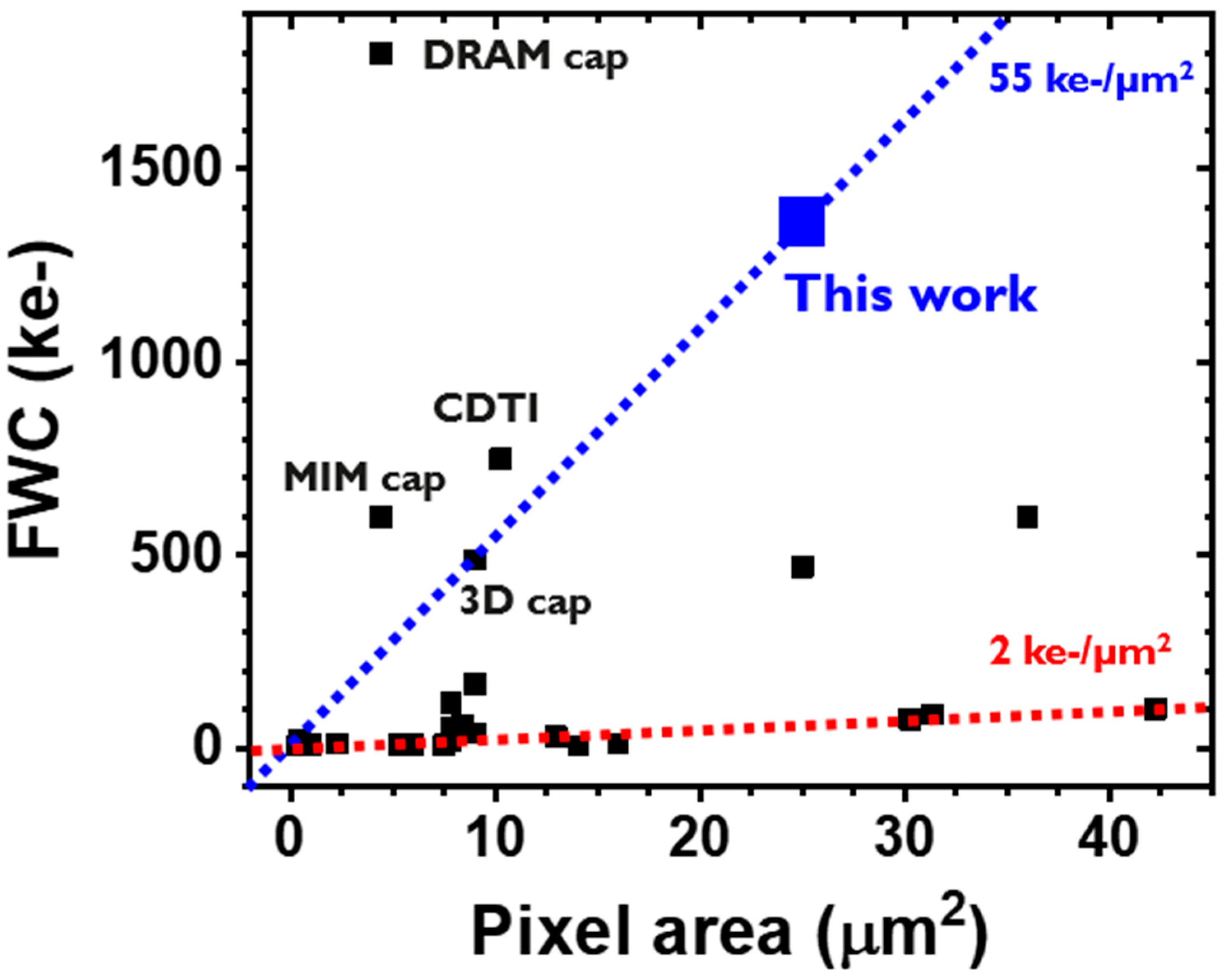
| Ref. | FWC (ke-) | Pixel Pitch (µm) | FWC Density (ke-/µm2) | Remarks |
|---|---|---|---|---|
| This work | 1367 | 5 | 55 | TF-PPD |
| [22] | 24,300 | 16 | 95 | LOFIT Trench cap |
| [23] | 750 | 3.2 | 73 | CDTI, hole collection |
| [24] | 103 | 6.5 | 2 | - |
| [25] | 12 | 1 | 12 | - |
| [26] | 20 | 2.8 | 3 | - |
| [27] | 10 | 0.6 | 28 | - |
| [28] | 8 | 2.4 | 1 | - |
| [29] | 120 | 2.8 | 15 | - |
| [30] | 20 | 0.64 | 49 | - |
| [31] | 76 | 5.5 | 3 | - |
| [32] | 13 | 1.5 | 6 | - |
| [33] | 55 | 2.8 | 7 | - |
| [34] | 10 | 2.74 | 1 | - |
| [35] | 88 | 5.6 | 3 | - |
| [36] | 30 | 3.6 | 2 | - |
| [37] | 12 | 2.3 | 2 | - |
| [38] | 40 | 3 | 4 | - |
| [39] | 60 | 2.9 | 7 | - |
| [40] | 1800 | 2.1 | 408 | DRAM cap |
| [41] | 600 | 2.1 | 136 | MIM cap |
| [42] | 166 | 3 | 18 | Dual PD |
| [5] | 470 | 5 | 19 | TFPD Junction cap |
| [43] | 10 | 2.45 | 2 | - |
| [44] | 489 | 3 | 54 | 3D cap |
| [45] | 8 | 3.75 | 1 | - |
| [46] | 600 | 6 | 17 | TFPD Junction cap |
Disclaimer/Publisher’s Note: The statements, opinions and data contained in all publications are solely those of the individual author(s) and contributor(s) and not of MDPI and/or the editor(s). MDPI and/or the editor(s) disclaim responsibility for any injury to people or property resulting from any ideas, methods, instructions or products referred to in the content. |
© 2023 by the authors. Licensee MDPI, Basel, Switzerland. This article is an open access article distributed under the terms and conditions of the Creative Commons Attribution (CC BY) license (https://creativecommons.org/licenses/by/4.0/).
Share and Cite
Kim, J.H.; Berghmans, F.; Siddik, A.B.; Sutcu, I.; Monroy, I.P.; Yu, J.; Weydts, T.; Georgitzikis, E.; Kang, J.; Baines, Y.; et al. A Thin-Film Pinned-Photodiode Imager Pixel with Fully Monolithic Fabrication and beyond 1Me- Full Well Capacity. Sensors 2023, 23, 8803. https://doi.org/10.3390/s23218803
Kim JH, Berghmans F, Siddik AB, Sutcu I, Monroy IP, Yu J, Weydts T, Georgitzikis E, Kang J, Baines Y, et al. A Thin-Film Pinned-Photodiode Imager Pixel with Fully Monolithic Fabrication and beyond 1Me- Full Well Capacity. Sensors. 2023; 23(21):8803. https://doi.org/10.3390/s23218803
Chicago/Turabian StyleKim, Joo Hyoung, Francois Berghmans, Abu Bakar Siddik, Irem Sutcu, Isabel Pintor Monroy, Jehyeok Yu, Tristan Weydts, Epimitheas Georgitzikis, Jubin Kang, Yannick Baines, and et al. 2023. "A Thin-Film Pinned-Photodiode Imager Pixel with Fully Monolithic Fabrication and beyond 1Me- Full Well Capacity" Sensors 23, no. 21: 8803. https://doi.org/10.3390/s23218803
APA StyleKim, J. H., Berghmans, F., Siddik, A. B., Sutcu, I., Monroy, I. P., Yu, J., Weydts, T., Georgitzikis, E., Kang, J., Baines, Y., Hermans, Y., Chandrasekaran, N., De Roose, F., Uytterhoeven, G., Puybaret, R., Li, Y., Lieberman, I., Karve, G., Cheyns, D., ... Lee, J. (2023). A Thin-Film Pinned-Photodiode Imager Pixel with Fully Monolithic Fabrication and beyond 1Me- Full Well Capacity. Sensors, 23(21), 8803. https://doi.org/10.3390/s23218803