Abstract
A gating circuit for a photonic quantum simulator is introduced. The gating circuit uses a large excess bias voltage of up to 9.9 V and an integrated single-photon avalanche diode (SPAD). Nine channels are monolithically implemented in an application-specific integrated circuit (ASIC) including nine SPADs using 0.18 µm high-voltage CMOS technology. The gating circuit achieves rise and fall times of 480 ps and 280 ps, respectively, and a minimum full-width-at-half-maximum pulse width of 1.26 ns. Thanks to a fast and sensitive comparator, a detection threshold for avalanche events of less than 100 mV is possible. The power consumption of all nine channels is about 250 mW in total. This gating chip is used to characterize the integrated SPADs. A photon detection probability of around 50% at 9.9 V excess bias and for a wavelength of 635 nm is found.
1. Introduction
Avalanche photodiodes operated above their breakdown voltage (in the Geiger mode) are able to detect single photons and are therefore called single-photon avalanche diodes (SPADs). The SPAD is biased with a reverse voltage of VR = VBD + VEX, where VBD is the breakdown voltage and VEX is the so-called excess bias voltage. If a photon hits the SPAD, a detectable current is generated. This is possible because the electric field in the multiplication layer is so high that a single electron–hole pair can trigger a self-sustaining avalanche [1,2]. This avalanche needs to be quenched, i.e., the voltage across the SPAD has to be reduced to or below the breakdown voltage, to enable the SPAD to detect the next photon. The quenching is also important because the reverse current through the SPAD could rise to high values and damage the SPAD. After the dead time, the SPAD is again recharged to VBD + VEx and is ready to detect the next photon.
There are different methods of quenching SPADs, such as passive, active, mixed and gated [3]. Passive quenching is very simple because a high-value resistor in series to the SPAD reduces the reverse voltage of the SPAD if the current rises. After the quenching, the reverse voltage slowly increases again. Active quenching circuits almost immediately quench the SPAD after an avalanche is detected. Fast active quenching reduces the after-pulsing probability [4]. Mixed quenching circuits use the passive and the active part. In the gated mode, the SPAD is charged and quenched with a defined rate.
The gated mode is ideal if the arrival time of the photons is known and periodic [5,6,7]. The gating mode reduces possible dark counts and also reduces the after-pulsing probability (which would have been caused by prior photon absorptions or dark counts) compared to using an active quenching circuit) [8,9]. This mode is therefore best suitable for the detection of the outcoming photons of a quantum simulator [10].
Also important for the application of SPADs in a quantum simulator is a high photon detection probability (PDP) to increase the rate of valid calculations, since this rate depends on PDP to the power of the number of Qubits, i.e., number of photons (Supplementary Information in [11]). The PDP is known to increase with the excess bias voltage VEX [8,12]. However, DCR and APP also increase with VEX. The APP is proportional to the capacitance of the SPAD (more precisely to the total capacitance of the input node of the quencher or gater including the SPAD capacitance) [4]. With SPADs integrated on the quencher or gater chip, the input-node capacitance can be reduced by elimination of the bond pad capacitances, which would be present in the case of off-chip SPADs. Thus, there is a need for fast switching transistors, which favor a small-structure-size technology, and for high breakdown voltages. Both requirements necessitate a compromise and/or a sophisticated circuit topology like cascoding [13]. In recent years, we implemented cascoded switching transistors in active quenchers [14,15] and gaters [16], both in 0.35 µm CMOS technology, to increase the excess bias voltage far above the nominal supply voltage. In this work, we use 0.18 µm high-voltage CMOS and double cascoding for the realization of a gating chip with nine channels, each with an integrated SPAD, to obtain shorter rise and fall times. To the best of the authors’ knowledge, the proposed gating circuit is the first to use double cascoding and supply a maximum excess bias voltage of 9.9 V.
2. Gater Chip
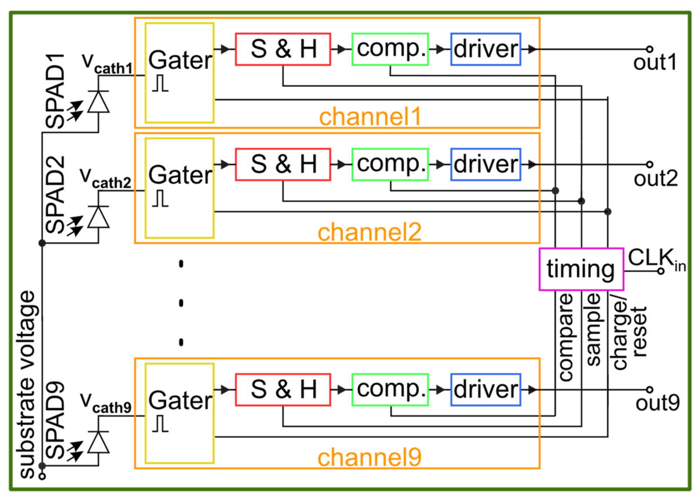
Figure 1 shows the simplified block diagram of the multi-channel gater chip. The proposed system consists of a timing section (violet) and nine separate channels (orange), which all include a double-cascoded gater switch (yellow), a sample and hold stage (red), a sensitive comparator (green) and a series of digital output drivers (blue). The circuit is designed with 1.8 V and 3.3 V MOSFETs in high-voltage 180 nm CMOS technology. The 3.3 V transistors are used to reach a voltage swing of 9.9 V at the cathodes of the SPADs and the faster 1.8 V transistors are employed for all other parts to ensure the best possible timing performance and to reduce power consumption. The driver section of every channel is split into multiple smaller drivers to send the signal across the hole chip with a total metal track length of about 5 mm for each channel. Directly next to the corresponding digital output bonding pad, an output driver is placed.
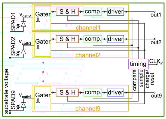
Figure 1.
Block diagram of gating chip with 9 channels and integrated SPADs.
The timing signals for every channel are generated in a central timing block (violet) and distributed via matched delay lines to the channels, which are up to 1 mm away from the timing block. Every channel has a separate bias voltage input for the comparator reference to cope with process and temperature variations. To adjust the performance of the sample and hold stages, a separate bias voltage is used, which is shared to all channels to reduce the number of necessary bond wires. The charging duration of the SPADs and the gating window duration can be adjusted via two separate bias voltages. These voltages control variable delays in the timing section and therefore affect all channels simultaneously. It is possible to charge the SPADs to a lower voltage (VEX < 9.9 V) and therefore also to reach shorter gating windows.
3. Structure of SPAD
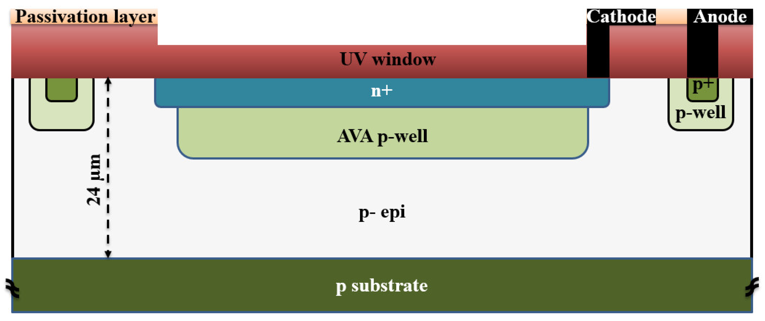
Figure 2 shows the cross-section of the integrated SPAD fabricated in a 0.18 μm high-voltage CMOS process. The SPAD comprises a shallow n+ region and a customized p-well avalanche region formed on a p-type doped epitaxial layer (p- epi) with a doping concentration of ~1.3 × 1013 cm−3 and a thickness of ~24 μm. The thick epi layer is advantageous for a low capacitance (i.e., low APP) and for a high PDP for red and near-infrared light. The diameter of the p-well (50 µm) is considered smaller than that of the n+ cathode (55 µm) to avoid early edge breakdown. An STI with a width of 10.1 µm separates the n+ cathode and the p+ anode ring.
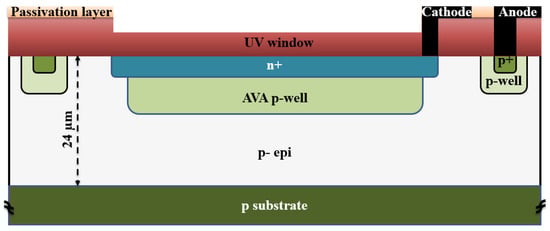
Figure 2.
Schematic cross section of the n+/avalanche-p-well CMOS SPAD (not to scale).
This design features a thick absorption region. When the device is reverse-biased beyond the breakdown voltage, a high electric field is formed at the n+/p-well junction that serves as an avalanche multiplication zone. At this voltage level, a weaker electric field expands from below the p/n junction through the p-well and through the p- epitaxial layer towards the substrate, which serves as the absorption region. All electrons photogenerated in the thick absorption region drift up to the p-well and will pass through the full thickness of the multiplication zone for impact ionization, resulting in a high PDP. The breakdown voltage of this device is 34.4 V according to simulations with Silvaco Atlas [17]. The simulated capacitance of the SPAD is 20 fF. Figure 3 shows a vertical cross-section of the electric field at an excess bias voltage of 10 V, as obtained through Geiger mode device simulation using Atlas.
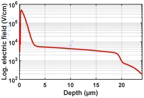
Figure 3.
A vertical cross-section of the electric field at the center of the structure at an excess bias of 10 V.
The electric field strength is larger than 3000 V/cm throughout the thick absorption zone/epitaxial layer. This results in an electron drift velocity larger than 4 × 106 cm/s, leading to a carrier collection time of less than 0.5 ns. Thus, a very short gating pulse at the nanosecond scale should be possible.
4. Gating Circuit
4.1. High-Voltage Cascode Switch
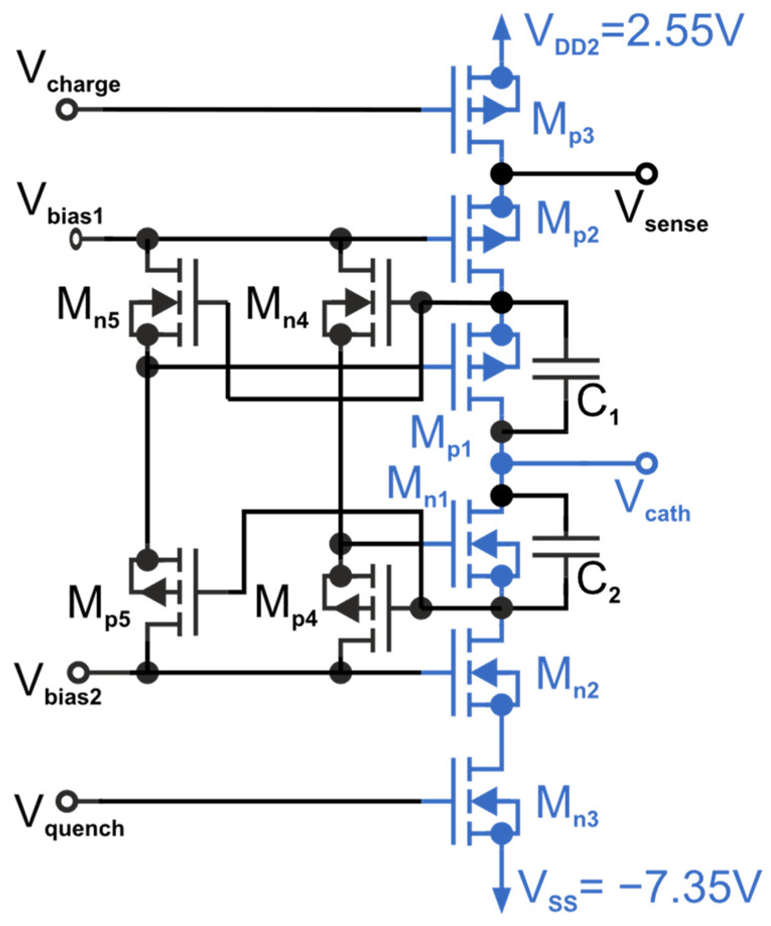
The proposed gating switch for a maximum excess bias of 9.9 V is shown in Figure 4 (marked blue; a modified version of the quenching switch of an active quencher realized in 0.35 µm CMOS and presented in [15]). It is a high-voltage double-cascoded switch (HVCS) with dual adaptive bias voltages. The simple adaptive gate bias of the second cascode transistor used in [15] had to be extended to the dual adaptive gate biasing with a separate adaptive bias with Mn4 and Mp4 for Mn1, as well as Mn5 and Mp5 for Mp1, to keep the voltages during the transition phases in their specified voltage limits. The HVCS is built with standard 3.3 V transistors. The bulks of the MOSFETs Mp1–Mp3 and Mn1–Mn2 are connected to their corresponding sources. The three stacked PMOS MOSFETs Mp1–Mp3 have to withstand 9.9 V, when the SPAD is quenched and the transistors Mn1–Mn3 pull the cathode to −7.35 V. The three stacked NMOS MOSFETs Mn1–Mn3 also have to sustain 9.9 V when the SPAD is charged to 9.9 V and waiting for a photon to arrive. Three transistors for each side are required since the nominal voltage of a single transistor is 3.3 V. The cathode of the SPAD is connected to Vcath and can therefore be switched between −7.35 V and 2.55 V (9.9 V swing). All transistors are isolated to substrate with deep n-wells. To save space, the MOSFETs Mn1–Mn3 as well as Mn5 and Mn4 are in the same deep n-wells. Due to the high voltage difference between the wells and the substrate all corners of the deep n-wells are rounded. The corners of the p-wells of the transistors Mn1, Mn2, Mn3, Mn4, and Mn5 are also rounded to withstand the occurring higher voltages than the nominal 8 V between the p-wells and the deep n-wells.
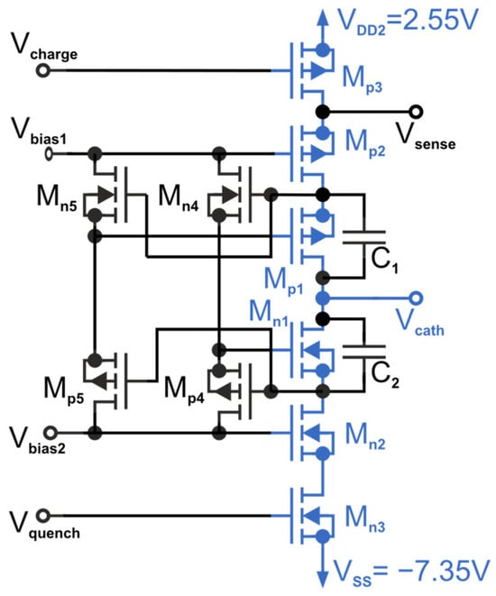
Figure 4.
High-voltage double-cascoded switch (HVCS) with dual adaptive bias shift.
If quenching is initiated (Vquench = Vbias2) and charging is deactivated (Vcharge = VDD2), the transistor Mn3 switches on and the transistor Mp3 switches off. The drains of Mn3 and Mp3 are discharged to −7.35 V and Vbias1 + VTh, respectively. The transistors Mn2 and Mp2, respectively, switch on and off because the gate of Mp2 is at a fixed bias voltage of Vbias1 = −0.75 V and the gate of Mn2 is at a fixed bias voltage of −4.05 V. The drain of Mn2 is discharged to Vss = −7.35 V. Therefore, the transistors Mp4 and Mp5 are in the on-state and shift the voltages on the gate of Mn1 and Mp1 to Vbias2 = −4.05 V. This shift at the gate of Mn1 sets this transistor into the on-state and discharges its drain, and therefore the Vcath output to −7.35 V. Because of the shift at the gate of Mp1 (caused by Mn4 and Mp4), the transistor Mp1 is now in the off-state. The adaptive bias circuitry (Mn4, Mn5, Mp4, Mp5) is necessary to keep the voltages on Mn1 and Mp2 in the process limits. To keep the potential difference on the transistors Mp1 and Mn1 during the fast-switching process also in the range of the absolute maximum voltages, two slightly different adaptive bias voltages with slightly different time behavior are used (dual adaptive bias; Mp5–Mn5 and Mp4–Mnp4). The capacitors C1 and C2 act in combination with the trace resistance as a snubber in [18] to suppress voltage peaks at the blue-marked transistors occurring during the transition between VDD2 and Vss. Without them, voltage peaks over 5 V would occur.
4.2. Sample and Hold and Comparator
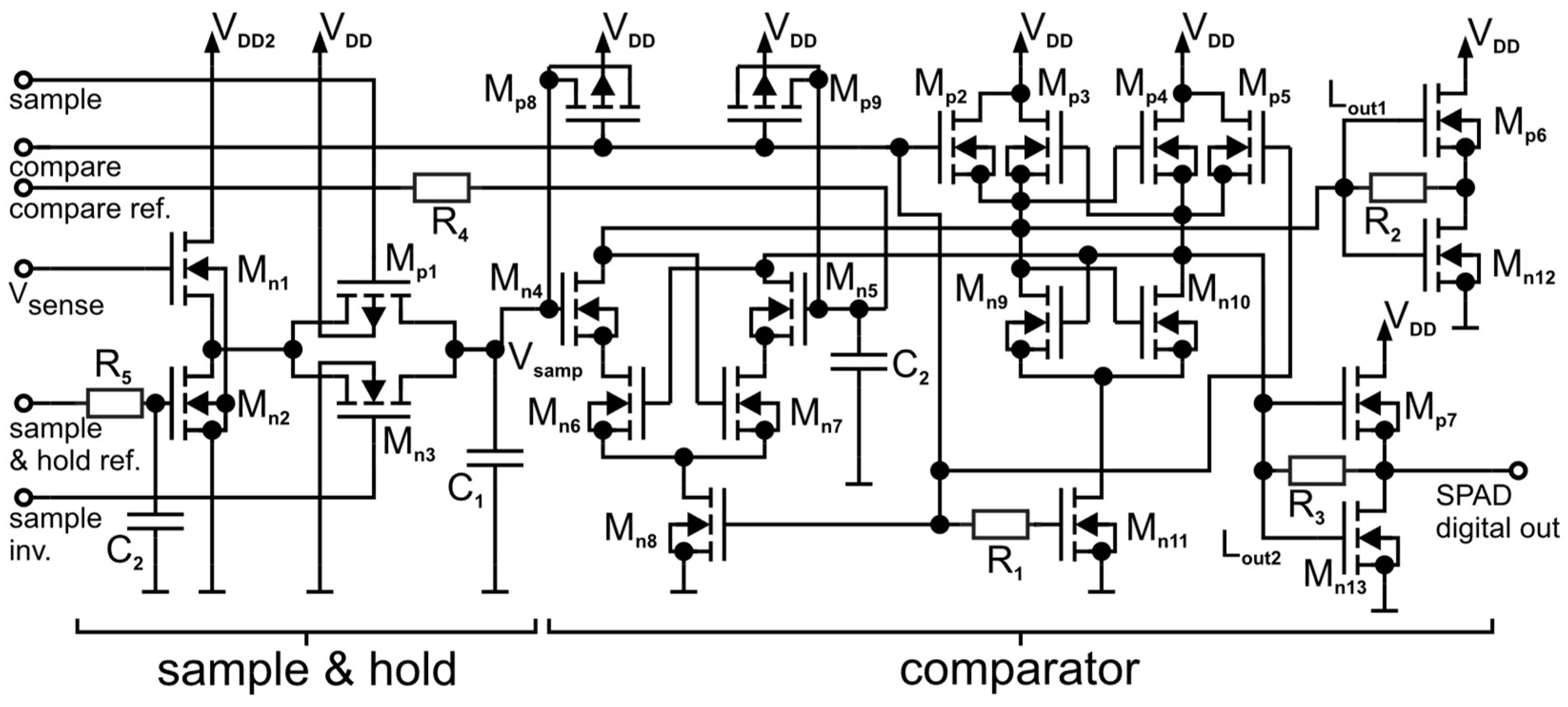
The next stage after the high-voltage cascode switch is the sample and hold circuitry, which is followed by the comparator stage as shown in Figure 5. The voltage on the SPADs cathode is indirectly sensed at the drain of Mp3 at the HVCS (Figure 4). The voltage range of Vsense is between Vbias1 = −0.75 V and VDD2 = 2.55 V, which is a 3.3 V range. To obtain the best possible timing performance and to save energy in the following stages, 1.8 V transistors are used, and only Mn1 in Figure 5 is therefore a 3.3 V MOSFET. A source follower with a current source load (Mn1 and Mn2) is used to shift the voltage range down into the range of 0 V–1.8 V. The “sample & hold ref.” bias input is used to control the current through the source follower and to shift the voltage externally to manage process, voltage, and temperature variations. All nine channels get the same reference voltage to reduce the needed number of pads. The resistor R5 and the capacitor C2 act as a low pass filter to reduce the noise and distortion coming from very long metal traces (up to 7 mm).

Figure 5.
Comparator-, sample- and hold stage-inclusive level shifting (Mn1 is a 3.3 V MOSFET; all other transistors are 1.8 V MOSFET).
The hold capacitance C1 is charged to approximately Vsense when the gating window is open, and the transmission gate Mn3/Mp1 conducts. The transmission gate (Mp1 and Mn3) is used to disconnect the capacitor C1 just before the SPAD is quenched to store the value of Vsense. The stored voltage Vsamp is an indicator if an avalanche was triggered because it indicates if Vsense and therefore Vcath were discharged due to an avalanche. The control signals “sample” and “sample inv.” are generated centralized for all channels in the timing section (see Figure 1). The signals are cross-coupled to ensure a simultaneous transition on both transistors of the transmission gate.
The proposed clocked high-speed comparator (modified compared to that realized in 65 nm CMOS and presented in [16]) is also shown in Figure 5 on the right side. It consists of a latch (Mp3, Mn9, Mp4, Mn10) with two reset MOSFETs Mp2 and Mp5, the input transistors Mn4 and Mn5, two cross-coupled MOSFETS Mn6 and Mn7, two tail transistors Mn8 and Mn11 and two output CMOS inverters with a feedback resistor (Mp6, Mn12, Mp7, Mn13). Only the output of one inverter (Mp7, Mn13) is used. The other is used to ensure a symmetrical load at the latch nodes (Lout1, Lout2). The resistive feedback at the CMOS inverters reduces the slope of the transfer characteristics and therefore reduces the risk of switching the next logic stage on and off multiple times during the decision phase.
In the reset phase (compare = 0 V), Mn8 and Mn11 are switched off and the transistors Mp2 and Mp5 reset the output nodes of the latch to VDD. In the compare phase (compare = VDD = 1.8 V), the reset transistors Mp2 and Mp5 are switched off and Mn8 and Mn11 are switched on to enable the input transistors to decide in which state the latch is pulled. Mn6 and Mn7 are switched on from the rest phase because their gates are pulled to VDD. Mn6 and Mn7 reduce the energy consumption by avoiding static current. In addition, the low-power process module was used. The input MOSFETs Mn4 and Mn5 discharge the nodes Lout1 and Lout2. The voltages at gates of Mn4 and Mn5 determine if Lout1 or Lout2 is discharged fast and determine therefore if the sampled voltage (Vsamp) or the reference voltage (compare ref.) is lower. When the reference voltage is higher than the sampled voltage Vsamp, the node Lou2 is discharged faster via Mn10 and Mn5. If the node Lout2 is equal to VDD–Vth (Vth of Mp3 and Mp4), Mp3 enters into the on mode and the complete latch switches because of the positive feedback to Lou1. The reference voltage is filtered and stabilized with the resistor R4 and the capacitor C2 which act as a low pass filter to reduce the noise and distortion coming from the very long metal traces. To compensate charge injection during the change from reset to the compare phase and therefore obtain a more sensitive comparator, Mp8 and Mp9 (MOSCAPs) inject charge during the transition for compensation purposes.
The clock for the comparator (compare) is centralized and generated for all channels in the timing section (see Figure 1). The compare phase is triggered approximately 1 ns after the transmission gate is closed to reduce distortions from the quenching process to achieve a higher sensitivity. The reset phase is triggered by the negative edge of the chip’s clock input to avoid distortions in the charging phase caused by the big digital output drivers on the chip. The resistor R1 causes a short delay between the gate of Mn11 and the other tail transistor Mn8 and the reset transistors (Mp2 and Mp5). This delay of the compare signal (clock) is caused by the resistance of R1 and the Mn11 gate capacitance. This short delay retards the discharging of Lout1 and Lout2 and therefore increases ΔU0, which increases the robustness of the latch against noise and mismatch. ΔU0 is the initial voltage difference at the latch nodes Lout1 and Lout2 which causes the latch to regenerate [19].
4.3. Layout
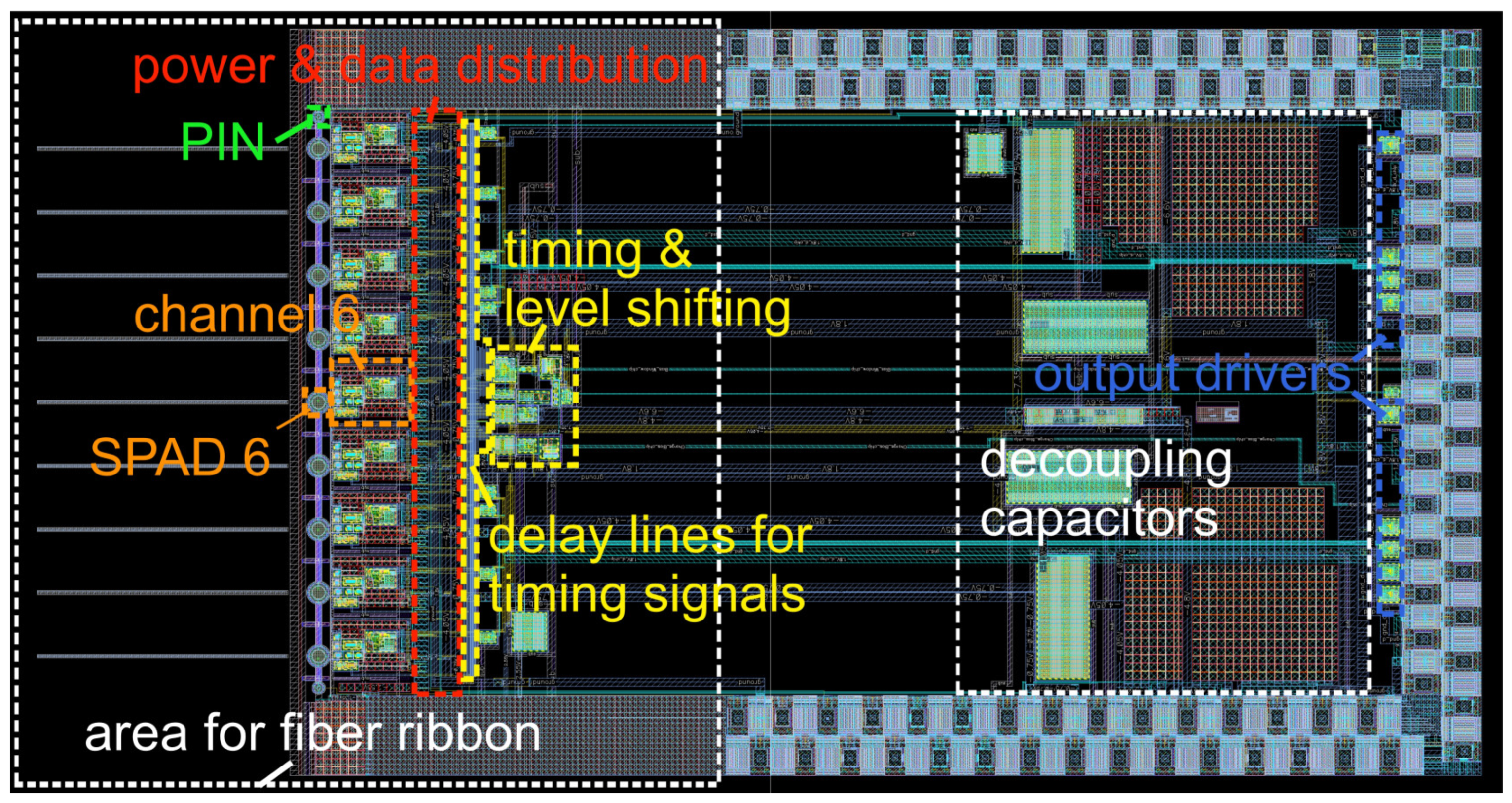
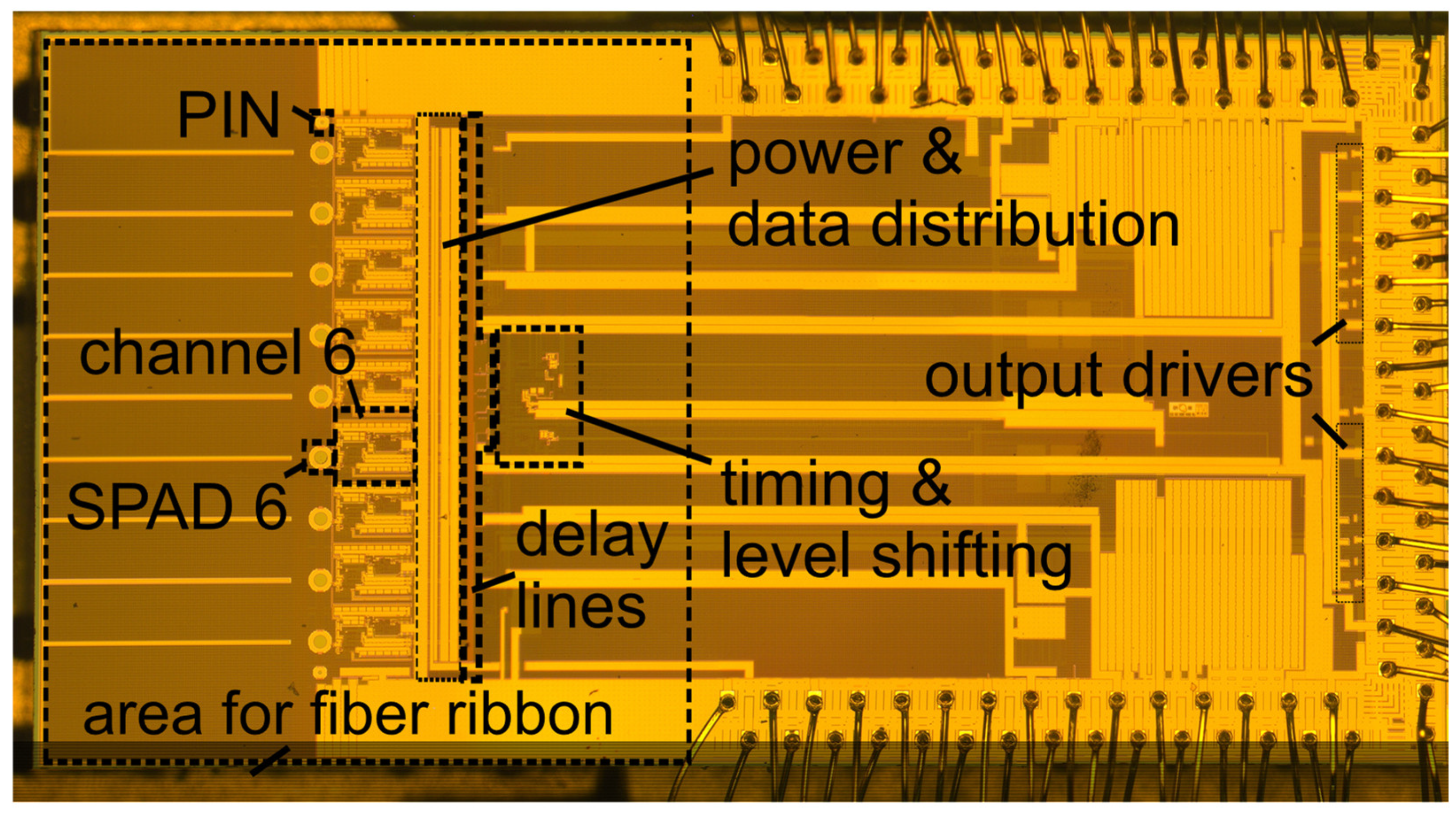
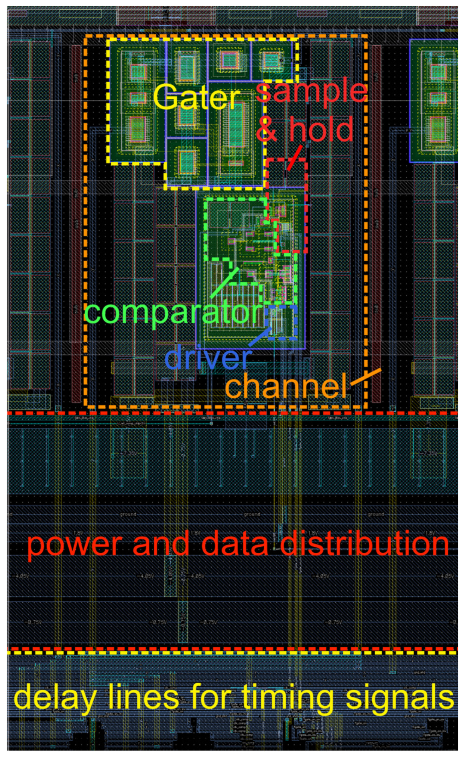
The gater ASIC with the nine integrated SPADs and for coupling the photons via a fiber ribbon into the SPADs has a chip size of about 5.8 × 3 mm2. The layout of the complete gater chip with integrated SPADs is presented in Figure 6. The chip photo of the fabricated ASIC is depicted in Figure 7. One gating circuit with an area of 380 × 640 μm2 is shown in Figure 8, including parts of the power and data distribution and the delay lines. Due to the fast, simultaneous switching of all channels, high current peaks occur. The various supply voltages are therefore stabilized with large arrays of metal capacitors (MIM) and MOS capacitors on the right side shown in Figure 6.
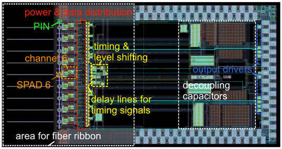
Figure 6.
Layout of the gater chip containing 9 integrated 50 µm SPADs.
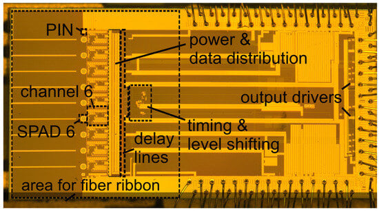
Figure 7.
Photo of the complete multi-channel gating chip with bonding wires.

Figure 8.
Layout of one gater channel.
The SPADs are placed at a spacing (pitch) of 256 µm to ensure that the intended fiber ribbon [20] fits on the chip. The fiber ribbon is the reason why the ASIC is much bigger than it would normally be because of the layout of the circuit blocks alone. The end of the fiber ribbon is mounted close to the surface of the gater ASIC for complete coupling of the light from the fiber cores into the SPADs. Therefore, bond wires and bond pads are not allowed in the area reserved for the fiber ribbon. The end of the fiber ribbon has dimensions of 10 mm × 4.25 mm. Figure 6 shows the layout of the gater ASIC with the integrated SPADs having a diameter of 50 μm. Two PIN photodiodes for easing the adjustment of the fiber ribbon are placed one at each end of the line of the nine SPADs at a distance of 127 μm. Figure 7 shows a chip photo of the gating chip glued on a PCB including the connected gold bond wires without the fiber ribbon.
4.4. Post-Layout Simulations
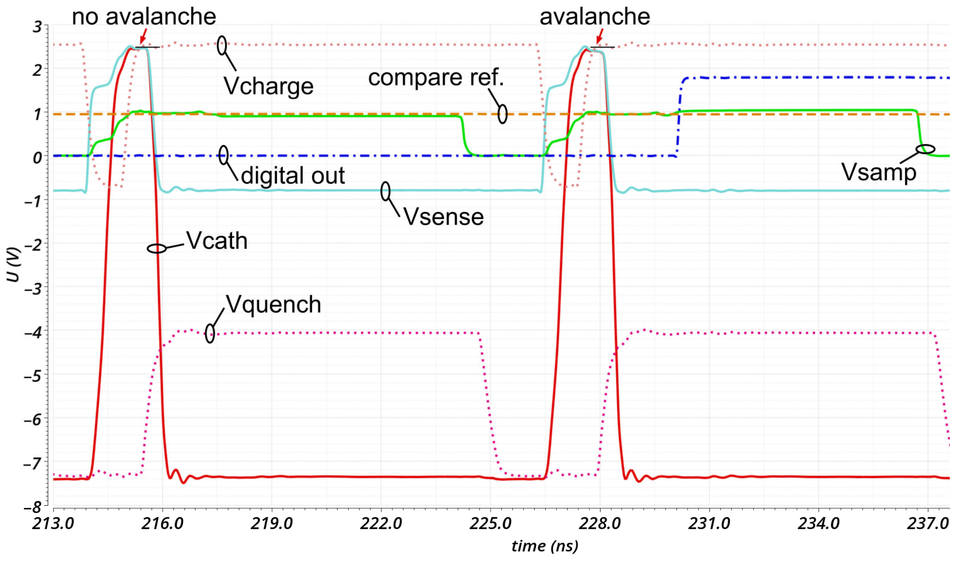
Figure 9 shows the transient of the cathode’s voltage (red), the input of the source follower Vsense (turquoise), the output of the sample and hold stage Vsamp (green), the comparator’s digital output (blue), the comparator’s reference voltage (compare ref., orange), the quenching trigger signal Vquench (dotted violet) and the charging trigger signal Vcharge (dotted red) as a post-layout simulation. Due to the fully integrated design, it is not possible to measure the real transient signals.
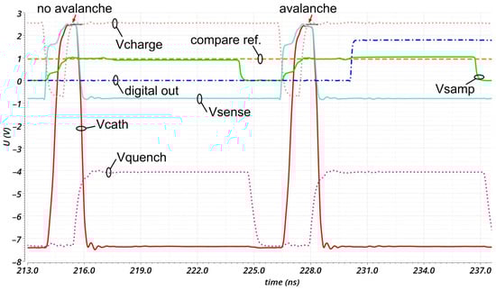
Figure 9.
Transients at important nodes obtained by post-layout simulation.
The cathode of the SPAD is charged to 2.55 V if it is “on” and quenched to −7.55 V. The gater switch has a 10% to 90% rise time of 480 ps and a fall time of 280 ps. The swing is 9.9 V. The full width at half maximum is 1.26 ns, but can be adjusted (increased) externally with a bias voltage. Also, the charging duration can be externally adjusted with a bias voltage. The proposed channels achieve a detection sensitivity of better than 100 mV at the SPADs cathode. All channels are fully synchronized to the input clock (CLKin shown in Figure 1) and all open the gating window at the same time with a jitter of less than 50 ps. This is ensured in the timing block with a delay network and delay lines. The input clock can be up to 150 MHz. The digital output drivers can drive 50 Ohm loads. The total power dissipation of the hole ASIC is less than about 250 mW at a gating frequency of 80 MHz.
5. Characterization of SPAD
The measurement setup is derived from the one presented in [21] and controlled by a PXI system from National Instruments (NI, Austin, TX, USA), comprised of the chassis NI-PXIe-1082 and the controller NI PXIe-8840 (NI), as depicted in Figure 10. Additionally, this system contains a FlexRIO FPGA card (NI PXIe-7972R), which allows streaming sampling data of a digitizer card (NI-PXIe-5162) with 625 MS/s in real time. This FPGA (field-programmable gate array) was used to extract the pulses at the output of the gater and to derive the pulse statistics for plotting the dark count rate (DCR) as well as the after-pulsing probability (APP). The APP was extracted from the inter-arrival time histograms during the dark measurements [21].
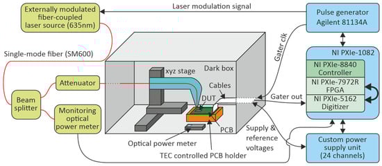
Figure 10.
Measurement setup for characterizing the SPADs in connection with the gater chip.
The gater chip was bonded onto a printed circuit board (PCB) using an FR4 substrate. The temperature of the gater chip was regulated to 25 °C by means of a thermoelectric cooler. Stabilizing the temperature is crucial for the characterization of SPADs, because the breakdown voltage as well as the dark count rate are particularly strongly temperature-dependent [21].
The PCB containing the gater was placed inside a dark box to block the background light. Light can be coupled into the SPADs on the gater chip using a single-mode fiber (SM600 from Thorlabs, Newton, NJ, USA). The mode field diameter of this fiber is in the range of 5µm and therefore considerably smaller than the active area of the SPAD, guaranteeing that almost all of the light is coupled into the active area. For adjusting the fiber output position on top of the SPAD, an xyz stage from Thorlabs (MTS50) was utilized.
The optical power at the output of the fiber was monitored by an optical power meter (Thorlabs PM100USB with Thorlabs S150C sensor) outside the dark box, connected to one output of a splitter, where the second output is connected to the fiber for the SPAD. The splitting ratio between these two outputs was set to 1125:1 by means of an optical attenuator in the splitting arm going to the SPAD. This large splitting ratio is required to have sufficient optical power at the optical power meter without saturation of the SPAD. The splitting ratio was calibrated before measurement using a second optical power meter inside the dark box and by placing the fiber output on top of the sensor head using the xyz stage.
A custom-built fiber-coupled laser at 635 nm was used as a light source. This laser was externally modulated by an electro-optic modulator from Jenoptic (AM635, Jena, Germany). Due to the availability of this fast light source with a high extinction ratio, the SPAD was only characterized at that wavelength. The achieved extinction ratio during the measurements was in the range of 100. The laser source was modulated by 2 ns long pulses with a repetition rate of 15 MHz. Please note, due to the limited extinction ratio, the monitored optical power does not only contain the optical power during the light pulse but also the pulse pause. This causes the optical power during the pulse to be overestimated, which results in underestimation of the extracted photon detection probability (PDP). The mean photon rate during the characterization of the PDP was set to 255,000 photons/s.
The relatively low repetition rate of 15 MHz was chosen in order to keep the after-pulsing probability low. The modulation signal for the laser, as well as the gating signal for the gaters, are generated by a pulse generator (Agilent 81134A, Santa Clara, CA, USA), which also allows accurately adjustment of the delay between these two signals, to optimize the overlap of the gating window with the arrival of the laser pulses at the SPADs.
The gating window was set to a length of ~4.5 ns, the reference voltage was optimized for each channel separately, and the substrate voltage Vsub was swept from −32 V to −43 V.
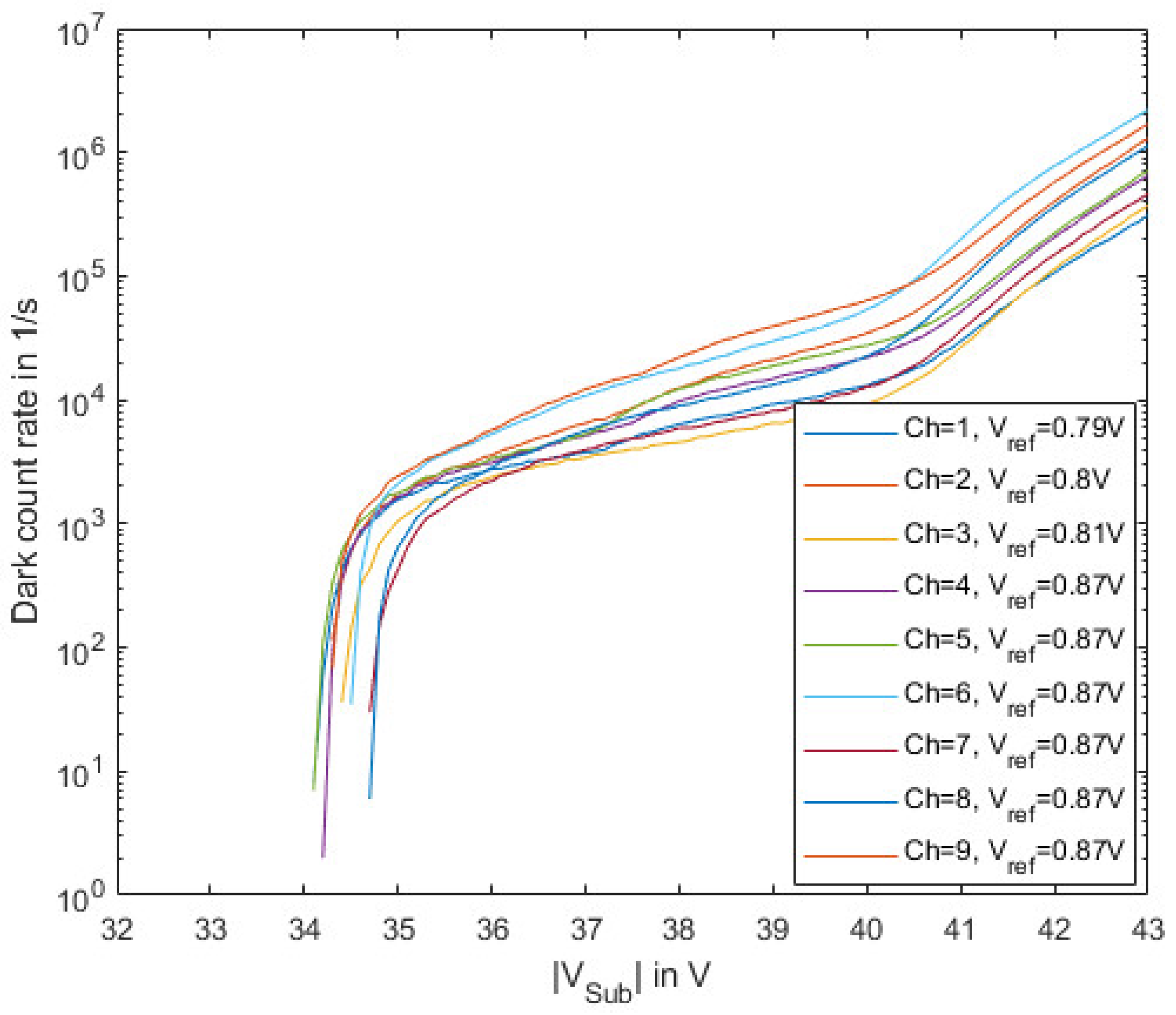
The dark count rate (DCR) as well as the after-pulsing probability (APP) were measured in dark conditions with a deactivated laser source. The reference voltages of the different channels were optimized for each specific channel.
Figure 11 shows the extracted dark count rate for the nine different channels of one gater ASIC reaching values of a few thousand to a few ten thousand counts per second in the useful operating range. It is important here to mention that the device was characterized at room temperature (25 °C). By cooling the device, the DCR can be reduced significantly, as, e.g., shown in [21]. The breakdown voltage varies by less than 1 V between the different channels. A different reference voltage for every channel can be set to achieve the best possible performance especially with respect to PDP and DCR. A larger reference voltage corresponds to a smaller detection threshold and therefore allows increasing the PDP, because also very small pulses can be detected. However, if the detection threshold is too small, noise (thermal noise and mainly power supply noise) at the input of the comparator will also generate an output signal, which would result in an increase in DCR and APP. Therefore, for each channel, the reference voltage was increased as much as possible (be aware that a larger reference voltage reduces the detection threshold) before the comparator was triggered (significantly) by noise. The first three channels (see Figure 11) need a slightly lower reference voltage Vref, which seems to have a systematic origin (e.g., differences in the supply of the channels due to unequal on-chip series resistances). Since the reference voltages are adjustable independently for each channel, this does not degrade the overall performance.

Figure 11.
Dark count rate (DCR) depending on the substrate voltage for the nine channels of the gater chip at room temperature (25 °C).
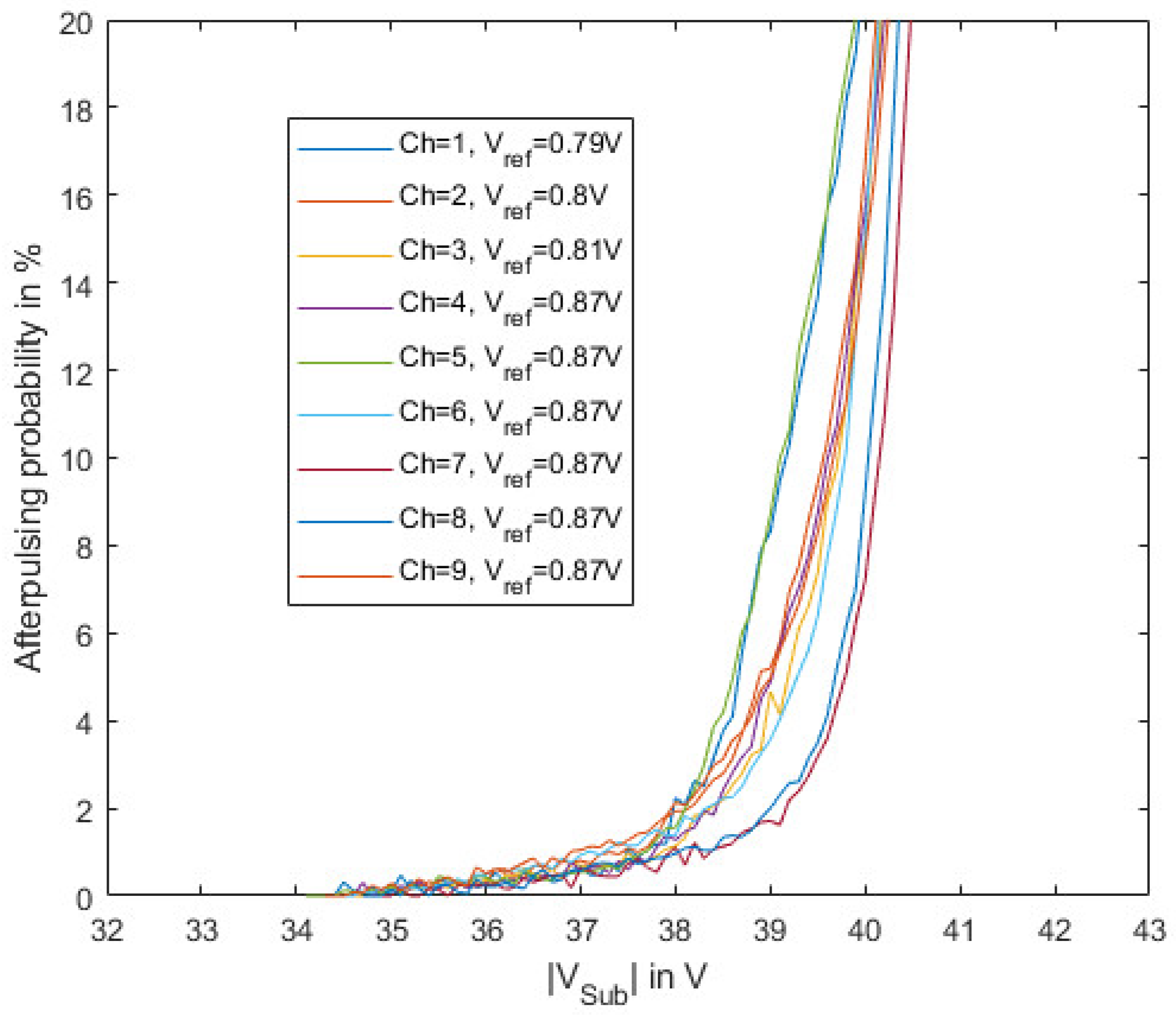
The after-pulsing probability was extracted by characterizing the distribution of the interarrival times between two consecutive pulses similar as in [21] and is shown in Figure 12. The resulting after-pulsing probability is quite low in the useful operating range. After-pulsing strongly depends on the dead time of the device. Therefore, further reducing the repetition rate of the gating pulses could further improve the APP, while increasing the repetition rate will lead to an increase in APP.
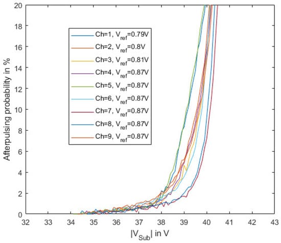
Figure 12.
After-pulsing probability (APP) depending on the substrate voltage for the nine channels of the gater chip at room temperature (25 °C).
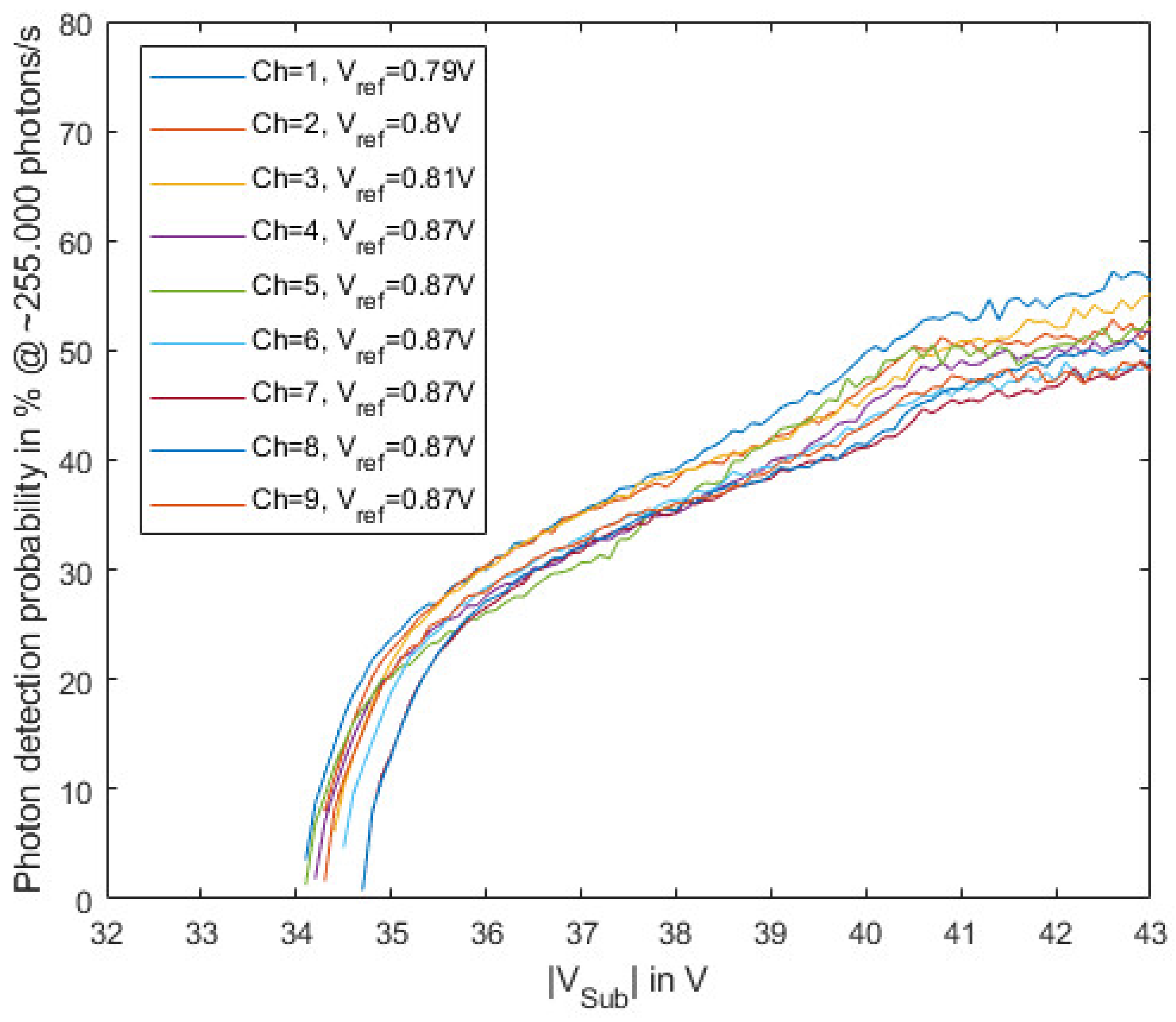
Figure 13 shows the extracted photon detection probability measured at a photon rate of ~255,000 photons/s. The saturation effects of the gater, as well as the influence of after-pulsing probability and dark count rate, were corrected. The limited extinction ratio of the laser was not corrected, since photons absorbed during the pulse pause might still contribute to the pulse rate if the generated charge carriers are diffusing to the absorption region while the gate window is active. Therefore, the plotted PDP will be slightly underestimated. Differences between the channels can, e.g., be explained by different transmission coefficients through the oxide stack. The SPADs in this chip do not have an anti-reflection coating, resulting in interference effects in the oxide stack, which results in a strongly wavelength-dependent PDP [22]. Due to thickness variations in the different layers in the oxide stack, this dependence can be different for the different channels. Furthermore, there is a large difference in the optical transmission between interference maxima and minima, which can occur for a certain wavelength due to oxide thickness tolerances from process run to process run or from wafer to wafer. The location of the interference maxima and minima in the spectrum can also change from run to run and wafer to wafer.
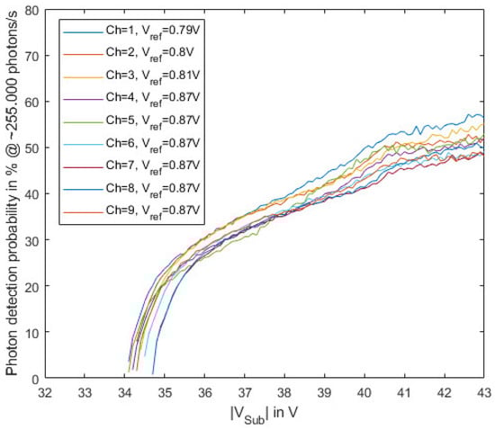
Figure 13.
Photon detection probability (PDP) depending on the substrate voltage for the nine channels of the gater chip at room temperature (25 °C) and at a photon rate of ~255,000 photons/s with 635 nm laser source.
The measurement of DCR and the APP show that the channels behave similarly. The deviations depend on different defect densities within the SPADs. The differences in the PDP might indicate the tolerance of the ion implantation dose in the avalanche layer.
The achieved PDP was considerably higher than, e.g., the PDP of ~35% at 635 nm in [14], where 0.35 µm CMOS technology was used, but the maximum excess bias voltage was limited to 6.6 V.
6. Comparison and Conclusions
Compared to the gating circuit in the 0.35 µm CMOS exploiting simple cascoding with a maximum excess bias voltage of 6.6 V [16] and a PDP similar to that of [14] (35%), the excess bias voltage was increased to 9.9 V, raising the PDP to about 50%. In addition, the power consumption of the gater switch, comparator and output driver of [16] was about 60 mW at 100 MHz, compared to 27.8 mW per channel of the 0.18 µm CMOS gating circuit presented here. The simulated fall time for quenching from 90% to 10% of 0.28 ns corresponds to a quenching slew rate of 28.3 V/ns, which is an extraordinarily high value. The suggested gating circuit also performs better than the 0.35 µm SiGe BiCMOS gater of [23], where the comparator alone showed a switching time of 250 ps, the power consumption was 30 mW at 1 MHz count rate and the excess bias voltage was only 5 V.
The fast switching time and the short full width at half maximum of the gating pulses allow a high repetition rate of laser pulses for usage in a quantum simulator. Easy scaling of the gater chip to a higher number of channels, and therefore larger photon numbers and Q-bits, respectively, are possible.
The PDP of the integrated SPAD was much larger than the PDP of 25% of InGaAs SPADs at a 1.55 µm wavelength [24], which were exploited for quantum simulator applications (Supplementary Information in [25]). The gater chip with the integrated SPADs therefore makes much better quantum simulators possible. The mismatch between the SPADs’ breakdown voltages should be reduced and an anti-reflection coating would be highly desirable to eliminate the influence of process tolerances on the photon detection probability. Also, a reduction in the dark count rate and in the after-pulsing probability, especially above about 6 V excess bias voltage, is desirable. In a redesign, the need for different reference voltages of some channels should be eliminated to proceed with only one bond pad for Vref.
Author Contributions
Conceptualization, H.Z. and B.G.; circuit design, C.R. and K.S.-H.; measurements, M.H.; device simulations, S.S.K.P.; implementation of avalanche layer, A.Z.; writing—original draft preparation, C.R., M.H. and S.S.K.P.; writing—review and editing, H.Z.; supervision, H.Z.; project administration, H.Z.; funding acquisition, H.Z. All authors have read and agreed to the published version of the manuscript.
Funding
This research was funded by the European Commission in the project EPIQUS, grant number 899368.
Institutional Review Board Statement
Not applicable.
Informed Consent Statement
Not applicable.
Data Availability Statement
Data are contained within the article.
Acknowledgments
We would like to thank the partners of the EPIQUS project for their cooperation and D. Sommer from X-FAB in Erfurt for enabling the modification of the avalanche layer.
Conflicts of Interest
Author Alexander Zimmer was employed by the company X-FAB. The remaining authors declare that the research was conducted in the absence of any commercial or financial relationships that could be construed as a potential conflict of interest.
Abbreviation
| SPAD | single-photon avalanche diode |
| ASIC | application-specific integrated circuit |
| PDP | photon detection probability |
| CMOS | complementary metal-oxide semiconductor |
| MOSFET | metal–oxide semiconductor field-effect transistor |
| APP | after-pulsing probability |
| HVCS | high-voltage double-cascoded switch |
| MIM capacitor | metal insulator metal capacitor |
| DCR | dark count rate |
| PCB | printed circuit board |
| PDP | photon detection probability |
References
- Cova, S.; Ghioni, M.; Lacaita, A.; Samori, C.; Zappa, F. Avalanche photodiodes and quenching circuits for single-photon detection. Appl. Opt. 1996, 35, 1956–1976. [Google Scholar] [CrossRef] [PubMed]
- Liu, J.; Jiang, W.; Kumar, S.; Deen, M.J. Time-Controlled SPAD Receivers in Optical Wireless Communication System. IEEE Photonics J. 2023, 15, 7304113. [Google Scholar] [CrossRef]
- Gallivanoni, A.; Rech, I.; Ghioni, M. Progress in Quenching Circuits for Single Photon Avalanche Diodes. IEEE Trans. Nucl. Sci. 2010, 57, 3815–3826. [Google Scholar] [CrossRef]
- Bronzi, D.; Tisa, S.; Villa, F.; Bellisai, S.; Tosi, A.; Zappa, F. Fast Sensing and Quenching of CMOS SPADs for Minimal Afterpulsing Effects. IEEE Photonics Technol. Lett. 2013, 25, 776–779. [Google Scholar] [CrossRef]
- Tosi, A.; Mora, A.D.; Della Frera, A.; Shehata, A.B.; Pifferi, A.; Contini, D. Fast-gated SPAD for ultra-wide dynamic range optical investigations. In Proceedings of the 2010 23rd Annual Meeting of the IEEE Photonics Society (Formerly LEOS Annual Meeting), Denver, CO, USA, 7–11 November 2010; pp. 185–186. [Google Scholar]
- Nissinen, I.; Nissinen, J.; Holma, J.; Kostamovaara, J. A TDC-based 4128 CMOS SPAD array for time-gated Raman spectroscopy. In Proceedings of the ESSCIRC 2014—40th European Solid State Circuits Conference, Venice Lido, Italy, 22–26 September 2014; pp. 139–142. [Google Scholar]
- Conca, E.; Cusini, I.; Severini, F.; Lussana, R.; Zappa, F.; Villa, F.A. Gated SPAD Arrays for Single-Photon Time-Resolved Imaging and Spectroscopy. IEEE Photonics J. 2019, 11, 6803910. [Google Scholar] [CrossRef]
- Renna, M.; Ruggeri, A.; Sanzaro, M.; Villa, F.A.; Zappa, F.; Tosi, A. High Detection Rate Fast-Gated CMOS Single-Photon Avalanche Diode Module. IEEE Photonics J. 2020, 12, 6802312. [Google Scholar] [CrossRef]
- Liu, J.; Jiang, W.; Deen, M.J. Time-Gated Circuit for SPAD-based OWC. In Proceedings of the 2022 IEEE Photonics Conference (IPC), Vancouver, BC, Canada, 13–17 November 2022; pp. 1–2. [Google Scholar]
- Aspuru-Guzik, A.; Walther, P. Photonic quantum simulators. Nat. Phys. 2012, 8, 285–291. [Google Scholar] [CrossRef]
- Wang, H.; Li, Y.-H.; Su, Z.-E.; Li, B.; Huang, H.-L.; Ding, X.; Chen, M.-C.; Liu, C.; Qin, J.; Li, J.-P.; et al. High-efficiency multiphoton boson sampling. Nat. Photonics 2017, 11, 361–365. [Google Scholar] [CrossRef]
- Webster, E.A.G.; Grant, L.A.; Henderson, R.K. A High-Performance Single-Photon Avalanche Diode in 130-nm CMOS Imaging Technology. IEEE Electron Device Lett. 2012, 33, 1589–1591. [Google Scholar] [CrossRef]
- Nam, H.; Ahn, Y.; Roh, J. 5-V buck converter using 3.3-V standard CMOS process with adaptive power transistor driver increasing efficiency and maximum load capacity. IEEE Trans. Power Electron. 2010, 27, 463–471. [Google Scholar] [CrossRef]
- Enne, R.; Steindl, B.; Hofbauer, M.; Zimmermann, H. Fast Cascoded Quenching Circuit for Decreasing Afterpulsing Effects in 0.35-μm CMOS. IEEE Solid State Circuits Lett. 2018, 1, 62–65. [Google Scholar] [CrossRef]
- Dervić, A. High-Voltage Active Quenching and Resetting Circuit for SPADs in 0.35 μm CMOS for raising the Photon Detection Probability. Opt. Eng. 2019, 58, 040501. [Google Scholar] [CrossRef]
- Goll, B.; Hofbauer, M.; Steindl, B.; Zimmermann, H. A Fully Integrated SPAD-Based CMOS Data-Receiver with a Sensitivity of −64 dBm at 20 Mb/s. IEEE Solid State Circuits Lett. 2018, 1, 2–5. [Google Scholar] [CrossRef]
- Silvaco Atlas User’s Manual. Available online: https://www.silvaco.com (accessed on 21 November 2023).
- Zach, F. Leistungselektronik Ein Handbuch, 5. Auflage; Springer: Berlin, Germany, 2015; ISBN 978-3-658-04898-3. [Google Scholar]
- Goll, B. Clocked, Regenerative Comparators in Deep-Sub-Micron CMOS. Ph.D. Thesis, TU Wien, Vienna, Austria, 2007. [Google Scholar]
- Fiber Ribbon, LaseOptics Corp. LF-SM-SC-01/2-780-HP-8CH/127-VG-FC/APC. Available online: https://www.laseoptics.com/Lensed-Tapered-Fibers-Description-2017.pdf (accessed on 10 September 2023).
- Hofbauer, M.; Steindl, B.; Zimmermann, H. Temperature Dependence of Dark Count Rate and After Pulsing of a Single-Photon Avalanche Diode with an Integrated Active Quenching Circuit in 0.35 μm CMOS. J. Sens. 2018, 2018, 9585931. [Google Scholar] [CrossRef]
- Poushi, S.S.K.; Mahmoudi, H.; Hofbauer, M.; Steindl, B.; Zimmermann, H. Photon Detection Probability Enhancement Using an Anti-Reflection Coating in CMOS-Based SPADs. Appl. Opt. 2021, 60, 7815–7820. [Google Scholar] [CrossRef]
- Ruggeri, A.; Ciccarella, P.; Villa, F.; Zappa, F.; Tosi, A. Integrated Circuit for Subnanosecond Gating of InGaAs/InP SPAD. IEEE J. Quantum Electron. 2015, 51, 4500107. [Google Scholar] [CrossRef]
- Signorelli, F.; Telesca, F.; Conca, E.; Della Frera, A.; Ruggeri, A.; Giudice, A.; Tosi, A. Low-Noise InGaAs/InP Single-Photon Avalanche Diodes for Fiber-Based and Free-Space Applications. IEEE J. Sel. Top. Quantum Electron. 2021, 28, 3801310. [Google Scholar] [CrossRef]
- Madsen, L.S.; Laudenbach, F.; Askarani, M.F.; Rortais, F.; Vincent, T.; Bulmer, J.F.F.; Miatto, F.M.; Neuhaus, L.; Helt, L.G.; Collins, M.J.; et al. Quantum computational advantage with a programmable photonic processor. Nature 2022, 606, 75–81. [Google Scholar] [CrossRef]


Disclaimer/Publisher’s Note: The statements, opinions and data contained in all publications are solely those of the individual author(s) and contributor(s) and not of MDPI and/or the editor(s). MDPI and/or the editor(s) disclaim responsibility for any injury to people or property resulting from any ideas, methods, instructions or products referred to in the content. |
© 2023 by the authors. Licensee MDPI, Basel, Switzerland. This article is an open access article distributed under the terms and conditions of the Creative Commons Attribution (CC BY) license (https://creativecommons.org/licenses/by/4.0/).