
The Total Ionizing Dose Effects on Perovskite CsPbBr3 Semiconductor Detector
Abstract
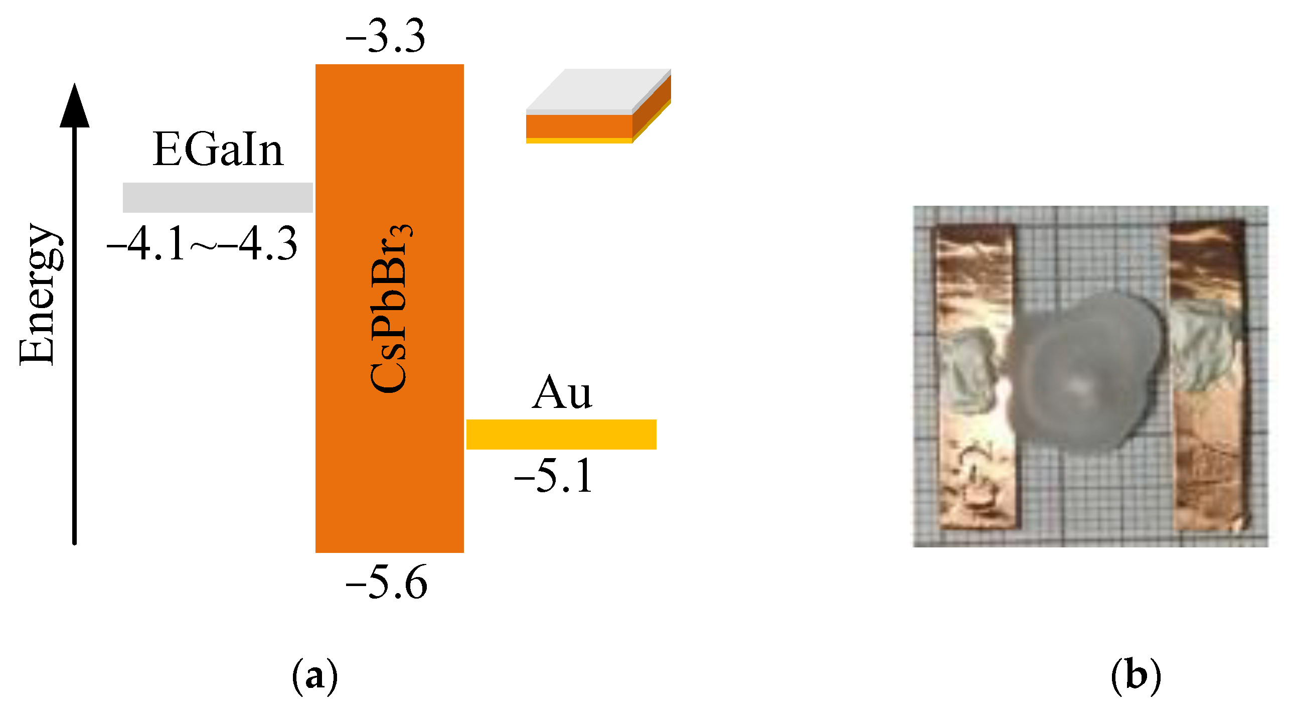
:1. Introduction
2. Materials and Methods
2.1. CsPbBr3 Detector Fabrication
2.2. Irradiation
2.3. Measurements
3. Results and Discussion
3.1. I-V and I-T Characteristics
3.2. γ-ray Spectral Performance
3.3. Photoluminescence
4. Discussion
5. Conclusions
Author Contributions
Funding
Institutional Review Board Statement
Informed Consent Statement
Data Availability Statement
Conflicts of Interest
References
- Schlesinger, T.E.; Toney, J.E.; Yoon, H.; Lee, E.Y.; Brunett, B.A.; Franks, L.; James, R.B. Cadmium zinc telluride and its use as a nuclear radiation detector material. Mater. Sci. Eng. R Rep. 2001, 32, 103–189. [Google Scholar] [CrossRef]
- Gehrels, N. The swift gamma-ray burst mission. AIP Conf. Proc. 2004, 727, 637–641. [Google Scholar]
- Nikl, M.; Yoshikawa, A. Recent R&D trends in inorganic single-crystal scintillator materials for radiation detection. Adv. Opt. Mater. 2015, 3, 463–481. [Google Scholar]
- Zhang, H.; Zhang, Z.; Ma, C.; Liu, Y.Q.; Xie, H.; Luo, S.; Yuan, Y.B.; Gao, Y.L.; Zhang, Y.; Ming, W.Q.; et al. Low Temperature Synthesis of All-Inorganic Perovskite Nanocrystals for UV-Photodetectors. J. Mater. Chem. C. 2019, 7, 5488–5496. [Google Scholar] [CrossRef]
- Ciavatti, A.; Sorrentino, R.; Basiricò, L.; Passarella, B.; Caironi, M.; Petrozza, A.; Fraboni, B. High-Sensitivity Flexible X-ray Detectors based on Printed Perovskite Inks. Adv. Funct. Mater. 2021, 31, 2009072. [Google Scholar] [CrossRef]
- Fraboni, B.; Ciavatti, A.; Merlo, F.; Pasquini, L.; Cavallini, A.; Quaranta, A. Organic semiconducting single crystals as next generation of low-cost, room-temperature electrical X-ray detectors. Adv. Mater. 2012, 24, 2289–2293. [Google Scholar] [CrossRef]
- Pecunia, V. Efficiency and spectral performance of narrowband organic and perovskite photodetectors: A cross-sectional review. J. Phys. Mater. 2019, 2, 042001. [Google Scholar] [CrossRef]
- Veeramalai, C.P.; Feng, S.; Zhang, X.; Pammi, S.V.N.; Pecunia, V.; Li, C. Lead–Halide perovskites for next-generation self-powered photodetectors: A comprehensive review. Photonics Res. 2021, 9, 968–991. [Google Scholar] [CrossRef]
- Rakita, Y.; Kedem, N.; Gupta, S.; Sadhanala, A.; Kalchenko, V.; Bohm, M.L.; Kulbak, M.; Friend, R.H.; Cahen, D.; Hodes, G. Low Temperature Solution-Grown CsPbBr3 Single Crystals and Their Characterization. Cryst. Growth Des. 2016, 16, 5717–5725. [Google Scholar] [CrossRef]
- He, Y.; Liu, Z.; McCall, K.M.; Lin, W.; Chung, D.Y.; Wessels, B.W.; Kanatzidis, M.G. Perovskite CsPbBr3 single crystal detector for alpha-particle spectroscopy. Nucl. Instr. Meth. Phys. Res. A 2019, 922, 217–221. [Google Scholar] [CrossRef]
- Liu, Y.; Zai, H.; Xie, H.; Liu, B.; Wang, S.; Zhao, Y.; Niu, D.; Huang, H.; Chen, Q.; Gao, Y. Effects of CsPbBr3 nanocrystals concentration on electronic structure and surface composition of perovskite films. Org. Electron. 2019, 73, 327–331. [Google Scholar] [CrossRef]
- Yu, J.; Liu, G.; Chen, C.; Li, Y.; Xu, M.; Wang, T.; Zhao, G.; Zhang, L. Perovskite CsPbBr3 crystals: Growth and applications. J. Mater. Chem. C 2020, 8, 6326–6341. [Google Scholar] [CrossRef]
- Zhang, B.B.; Wang, F.; Zhang, H.; Xiao, B.; Sun, Q.; Guo, J.; Hafsia, A.B.; Shao, A.; Xu, Y.; Zhou, J. Defect proliferation in CsPbBr3 crystal induced by ion migration. Appl. Phys. Lett. 2020, 116, 063505. [Google Scholar] [CrossRef]
- Peters, J.A.; Liu, Z.; Yu, R.; McCall, K.M.; He, Y.; Kanatzidis, M.G.; Wessels, B.W. Carrier recombination mechanism in CsPbBr3 revealed by time-resolved photoluminescence spectroscopy. Phys. Rev. B 2019, 100, 235305. [Google Scholar] [CrossRef]
- Stoumpos, C.C.; Malliakas, C.D.; Peters, J.A.; Liu, Z.; Sebastian, M.; Im, J.; Chasapis, T.C.; Wibowo, A.C.; Chung, D.Y.; Freeman, A.J.; et al. Crystal Growth of the Perovskite Semiconductor CsPbBr3: A New Material for High Energy Radiation Detection. Cryst. Growth Des. 2013, 13, 2722–2727. [Google Scholar] [CrossRef]
- He, Y.; Matei, L.; Jung, H.J.; McCall, K.M.; Chen, M.; Stoumpos, C.C.; Liu, Z.; Peters, J.A.; Chung, D.Y.; Wessels, B.W.; et al. High Spectral Resolution of Gamma-rays at Room Temperature by Perovskite CsPbBr3 Single Crystals. Nat. Commun. 2018, 9, 1609. [Google Scholar] [CrossRef]
- Fleetwood, D.M. Total Ionizing Dose Effects in MOS and Low-Dose-Rate-Sensitive Linear-Bipolar Devices. IEEE Trans. Nucl. Sci. 2013, 60, 1706–1730. [Google Scholar] [CrossRef]
- Fleetwood, D.M. Evolution of total ionizing dose effects in MOS devices with Moore’s law scaling. IEEE Trans. Nucl. Sci. 2018, 65, 1465–1481. [Google Scholar] [CrossRef]
- Schwank, J.R.; Shaneyfelt, M.R.; Fleetwood, D.M.; Felix, J.A.; Dodd, P.E.; Paillet, P.; Ferlet-Cavrois, V. Radiation effects in MOS oxides. IEEE Trans. Nucl. Sci. 2008, 55, 1833–1853. [Google Scholar] [CrossRef]
- Oldham, T.R.; McLean, F.B. Total ionizing dose effects in MOS oxides and devices. IEEE Trans. Nucl. Sci. 2003, 50, 483–499. [Google Scholar] [CrossRef]
- Bolotnikov, A.E.; Boggs, S.E.; Chen, C.H.; Cook, W.R.; Harrison, F.A.; Schindler, S.M. Properties of Pt Schottky type contacts on high-resistivity CdZnTe detectors. Nucl. Instr. Meth. Phys. Res. A 2002, 482, 395–407. [Google Scholar] [CrossRef]
- González, R.; Pérez, J.M.; Vela, O.; de Burgos, E.; Oller, J.C.; Gostilo, V. Electrical characterization of large volume CdZnTe coplanar detectors. Nucl. Instr. Meth. Phys. Res. A 2005, 547, 517–534. [Google Scholar] [CrossRef]
- Schlaus, A.P.; Spencer, M.S.; Miyata, K.; Liu, F.; Wang, X.; Datta, I.; Lipson, M.; Pan, A.; Zhu, X.Y. How lasing happens in CsPbBr3 perovskite nanowires. Nat. Commun. 2019, 10, 265. [Google Scholar] [CrossRef] [PubMed]
- He, Y.; Petryk, M.; Liu, Z.; Chica, D.G.; Hadar, I.; Leak, C.; Ke, W.; Spanopoulos, I.; Lin, W.; Chung, D.Y.; et al. CsPbBr3 perovskite detectors with 1.4% energy resolution for high-energy γ-rays. Nat. Photonics. 2021, 15, 36–42. [Google Scholar] [CrossRef]
- Miyata, K.; Meggiolaro, D.; Trinh, M.T.; Joshi, P.P.; Mosconi, E.; Jones, S.C.; Angelis, F.E.; Zhu, X.Y. Large polarons in lead halide perovskites. Sci. Adv. 2017, 3, 1701217. [Google Scholar] [CrossRef]
- Wei, K.; Xu, Z.; Chen, R.; Zheng, X.; Cheng, X.; Jiang, T. Temperature-dependent excitonic photoluminescence excited by two-photon absorption in perovskite CsPbBr3 quantum dots. Opt. Lett. 2016, 41, 3821–3824. [Google Scholar] [CrossRef]
- Liu, L.; Liu, A.; Bai, S.; Lv, L.; Jin, P.; Ouyang, X.P. Radiation Resistance of Silicon Carbide Schottky Diode Detectors in D-T Fusion Neutron Detection. Sci. Rep. 2017, 7, 13376. [Google Scholar] [CrossRef]
- Liu, L.; Li, F.; Bai, S.; Jin, P.; Cao, X.; Ouyang, X.P. Silicon carbide PIN diode detectors used in harsh neutron irradiation. Sens. Actuators A Phys. 2018, 280, 245–251. [Google Scholar] [CrossRef]


| Bias Voltage (V) | △Energy Resolution | ||
|---|---|---|---|
| −50 | −100 | −150 | |
| 100 krad(Si) | −1.18% | 6.42% | 5.57% |
| After annealing | 4.77% | -- | -- |
Disclaimer/Publisher’s Note: The statements, opinions and data contained in all publications are solely those of the individual author(s) and contributor(s) and not of MDPI and/or the editor(s). MDPI and/or the editor(s) disclaim responsibility for any injury to people or property resulting from any ideas, methods, instructions or products referred to in the content. |
© 2023 by the authors. Licensee MDPI, Basel, Switzerland. This article is an open access article distributed under the terms and conditions of the Creative Commons Attribution (CC BY) license (https://creativecommons.org/licenses/by/4.0/).
Share and Cite
Ma, W.; Liu, L.; Qin, H.; Gao, R.; He, B.; Gou, S.; He, Y.; Ouyang, X. The Total Ionizing Dose Effects on Perovskite CsPbBr3 Semiconductor Detector. Sensors 2023, 23, 2017. https://doi.org/10.3390/s23042017
Ma W, Liu L, Qin H, Gao R, He B, Gou S, He Y, Ouyang X. The Total Ionizing Dose Effects on Perovskite CsPbBr3 Semiconductor Detector. Sensors. 2023; 23(4):2017. https://doi.org/10.3390/s23042017
Chicago/Turabian StyleMa, Wuying, Linyue Liu, Haoming Qin, Runlong Gao, Baoping He, Shilong Gou, Yihui He, and Xiaoping Ouyang. 2023. "The Total Ionizing Dose Effects on Perovskite CsPbBr3 Semiconductor Detector" Sensors 23, no. 4: 2017. https://doi.org/10.3390/s23042017