Article

A High-Relative-Bandwidth Doherty Power Amplifier with Modified Load Modulation Network for Wireless Communications

1
School of Electronics and Information, Hangzhou Dianzi University, Hangzhou 310018, China
2
ECIT Institute, Queen’s University Belfast, Belfast BT3 9DT, UK
*
Author to whom correspondence should be addressed.
Sensors 2023, 23(5), 2767; https://doi.org/10.3390/s23052767
Submission received: 30 January 2023 / Revised: 27 February 2023 / Accepted: 1 March 2023 / Published: 2 March 2023
(This article belongs to the Collection RF and Microwave Communications)

Abstract

:
This paper presents a novel load modulation network to realize a broadband Doherty power amplifier (DPA). The proposed load modulation network consists of two generalized transmission lines and a modified coupler. A comprehensive theoretical analysis is carried out to explain the operation principles of the proposed DPA. The analysis of the normalized frequency bandwidth characteristic shows that a theoretical relative bandwidth of approximately 86% can be obtained across a normalized frequency range of 0.4–1.0. The complete design process that allows the design of the large-relative-bandwidth DPA based on derived parameter solutions is presented. A broadband DPA operating between 1.0 GHz and 2.5 GHz was fabricated for validation. Measurements demonstrate that the DPA can deliver an output power of 43.9–44.5 dBm with a drain efficiency of 63.7–71.6% in the 1.0–2.5 GHz frequency band at the saturation level. Moreover, a drain efficiency of 45.2–53.7% can be obtained at the 6 dB power back-off level.

1. Introduction

The rapid emergence of wireless communication applications that need to transmit large amounts of data such as wireless sensing networks has encouraged the development of RF front-end technology that can support high peak-to-average ratio (PAPR) signals with large bandwidth [1]. Power amplifiers (PAs) are required in modern wireless communication application systems to handle broad bandwidth (BW) and high PAPR simultaneously for the purpose of increasing data transmission rates. Traditional single-device PAs, such as class-F [2], class-E [3], and class-J [4], cannot meet the requirements of efficiently amplifying signals with high PAPR. Load modulation PAs, such as Doherty [5], out-phasing [6], and load modulation balance amplifiers (LMBAs) [7], can maintain high efficiency at the power back-off (OBO) level and are promising candidates for meeting the stringent linearity requirements. Currently, DPAs are widely used in wireless communications due to their easy-to-implement architecture [8,9]. However, the bandwidth of traditional Doherty PAs is restricted by impedance conversion networks, offset lines, matching networks, and package parameters of transistors [10,11,12,13]. Therefore, DPAs can only maintain the ideal performance at the OBO level in a narrow band. This bandwidth limitation greatly hinders the use of DPAs in RF transceivers that require high data BW and high PAPR.
Recently, some methods have been proposed to improve the bandwidth of Doherty PAs [14,15,16,17,18,19,20,21,22,23,24]. The finite impedance of the auxiliary PA branch at the OBO level is employed to enhance the OBO performance in a large bandwidth [14,15]. In addition, the introduction of complex load impedances to achieve better impedance conditions in a large bandwidth has been validated [16,17]. Post-matching techniques can reduce the impedance transformation ratio of output matching networks of main PA and auxiliary PA branches so as to provide larger bandwidth [18,19,20,21]. In addition, some continuous-mode PAs have been developed to have the ability to increase the impedance design space, thus widening the bandwidth of DPAs [22,23,24]. These technologies can ameliorate the impedance-matching condition of DPAs to expand the bandwidth of DPAs to a certain extent. However, due to the inherent limitations of a DPA’s load modulation network (LMN) structure, impedance mismatch at the OBO level is still inevitable. This will reduce the efficiency of the DPAs at the OBO level. Therefore, it is necessary to study a new LMN structure in order to realize more accurate impedance conversion at the OBO level in a large bandwidth while keeping Doherty load modulation behaviors.
A lot of effort has been made to realize larger bandwidth by altering the LMN structure of DPAs [25,26,27,28]. Recently, especially in [29,30], novel LMN structures have been proposed to extend the bandwidth, where the precise impedance can be realized using specific analysis at the OBO level. However, the relative bandwidth is still limited since both these analyses are based on traditional transmission lines, resulting in higher normalized frequency bands, such as 0.8–1.2 in [29] and 0.7–1.3 in [30].
In this paper, we propose a novel LMN structure including a modified coupler and two generalized transmission lines. The modified coupler is used in an LMN for the first time to achieve the required impedance such that the combination of the coupler and generalized transmission lines leads to an almost constant impedance at the OBO level in the lower normalized frequency band of 0.4–1, which means an ideal efficiency can be obtained in a larger relative bandwidth compared with previous works, e.g., [29,30]. A theoretical 86% relative bandwidth can be obtained when the proposed LMN is utilized. Furthermore, a more direct and straightforward analysis based on the normalized frequency and impedance condition immediately follows, from which the corresponding design parameters follow. This analysis allows the proposed LMN to be designed for practical situations, including different working frequencies and OBO levels. Compared with the previous broadband DPAs, the proposed DPA significantly expands the relative bandwidth. The structure of this paper is as follows: The theory of the proposed LMN is shown and the corresponding design equations are given in Section 2. Section 3 presents the complete design process, and simulations are given in detail. In Section 4, experiments are shown to validate the proposed DPA. The conclusions of this work are given in Section 5.

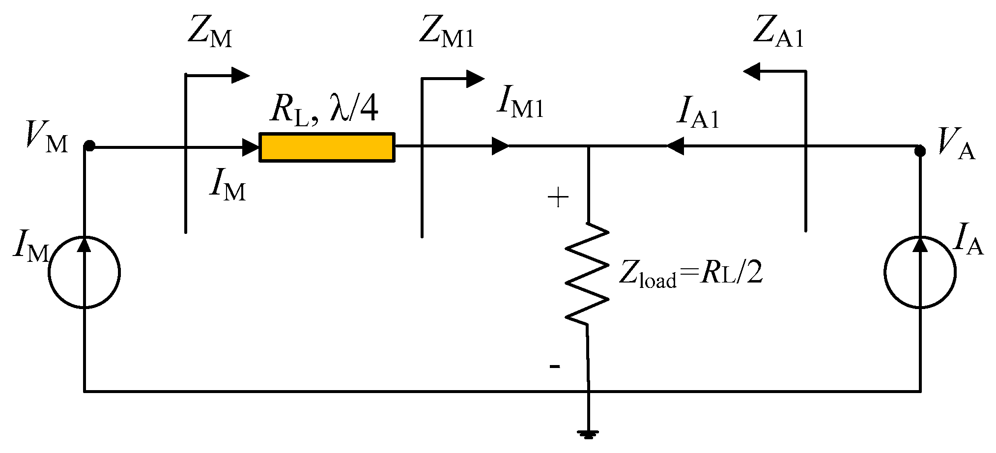
2. Analysis of DPA Theories

The conventional DPA topology is shown in Figure 1; here, the transistor is equivalent to an ideal current source. The conventional DPA has a main PA branch and an auxiliary PA branch, with a load of RL/2 at the combiner. In addition, a quarter-wavelength transmission line is used in the main PA branch in order to achieve impedance conversion [5]. According to the DPA theory [5], several impedance relationships are given as
Z M 1 , SAT = 2 · Z load
Z M 1 , OBO = Z load
Z A 1 , SAT = 2 · Z load
Z A 1 , OBO =
where ZM1 and ZA1 are the load impedances of the main and auxiliary PA branches, respectively. ZM and ZA represent the load impedances of devices for main and auxiliary PAs, respectively. The subscripts SAT and OBO refer to impedance conditions at the saturation and OBO levels, respectively. In the traditional DPA topology, the λ/4 line is responsible for converting the impedance well only at the center frequency, thus restricting the bandwidth of the resulting DPAs.
In this work, a modified load modulation network is proposed to address this issue, as shown in Figure 2a. In this scheme, the modified coupler is used to realize the impedance conversion at the main PA branch. The DPA load impedance is set to a complex value RL (1 + jX). The auxiliary PA branch also includes a generalized transmission line to represent the output network that is employed to obtain finite impedance ZA1,OBO (unlike that of infinity in traditional DPAs). The modified coupler structure shown in Figure 2b consists of a traditional branch line coupler and a reactance connected to port 2. Port 4 and port 1 are input and output terminals, respectively, while port 3 is open-circuited. The relationship between the four ports for this coupler arrangement is expressed as
V 1 V 2 V 3 V 4 = Z 0 0 + j j 2 0 + j 0 0 j 2 j 2 0 0 + j 0 j 2 + j 0 I 1 I 2 I 3 I 4
where V and I refer to the voltage and current of ports of the coupler. Subscripts 1, 2, 3, and 4 represent the port numbers. Z0 is the system impedance. Based on the condition of terminals shown in Figure 2b, the following relationships are obtained:
Z 2 = j Z 0 tan β l = j Z 0 tan π 2 f
I3 = 0
where β is the propagation constant. l is the physical length of the transmission line. Z2 represents the impedance of port 2.
As f is the normalized frequency, the relationship between the impedance of port 4 Z4 and the impedance of port 1 Z1 is derived as
Z 4 / Z 1 = 2 + j t a n π 2 f
As expressed in (8), Z4/Z1 has a constant resistance, as required for DPA synthesis [23]. Moreover, the resistance is independent of the normalized frequency f, which provides the possibility to realize operation in a lower normalized frequency band than the previous works [29,30]. Next, an analysis of this LMN and corresponding parameter solutions are given.

2.1. Power Back-Off Level

Figure 3 shows the equivalent schematic diagram of the main PA branch at the power back-off level. As shown in Figure 3, the load impedance of the main PA branch ZM1,OBO (Z1) is as follows:
Z M 1 , OBO = Z 1 = 1 + j X j X A 1 + j X + j X A = j X A X X A 1 + j X + X A R L
where XA refers to the normalized reactance of the auxiliary PA branch at the OBO level.
After substituting (9) to (8), the load impedance of the main PA transistor ZM,OBO (Z4) can be obtained as
Z M , OBO / R OPT = Z 4 / R OPT = 1 + j 0.5 t a n π 2 f j X A X X A 1 + j X + X A
where RL = 0.5ROPT.
In order to realize an OBO of 6 dB, the real part of Z4  R e ( Z 4 / R OPT ) should be set equal to 2. Then, we can deduce the following two expressions about XA:
X A = t a n π 2 f + X 2 t a n π 2 f + 4 X + t a n π 2 f + X 2 t a n π 2 f + 4 X 2 4 X t a n π 2 f 2 + 2 X 2 4 X t a n π 2 f
X A = t a n π 2 f + X 2 t a n π 2 f + 4 X t a n π 2 f + X 2 t a n π 2 f + 4 X 2 4 X t a n π 2 f 2 + 2 X 2 4 X t a n π 2 f
Figure 4a,b display the relationships expressed by (11) and (12), respectively. Based on Figure 4, we can now choose the appropriate XA and X to realize the desired OBO, in this case, 6 dB, for different values of f. Indeed, we can let R e ( Z 4 / R OPT ) be equal to a different value for obtaining different OBO values if desired. For example, an OBO of 9 dB can be obtained by setting R e ( Z 4 / R OPT ) = 4.
As shown in Figure 4, there are two solutions for X and XA in the normalized frequency band of 0.4–1.6. This provides more freedom to satisfy the impedance requirements of DPAs at the specified saturation level. Moreover, the value of XA changes sharply around f = 1. This variation hinders the realization of ultra-wideband DPAs in the normalized frequency range of 0.4–1.6. Therefore, the proposed topology can theoretically only achieve wideband DPA in the 0.4–1.0 or 1.0–1.6 frequency range. In order to obtain the maximum relative bandwidth, this paper chooses the frequency range of 0.4–1.0 for the following analysis and design.

2.2. Saturation Level

Figure 5 shows the equivalent schematic diagram of the main PA branch at the saturation level. The load impedance of the main PA branch is 2RL(1 + jX). According to the DPA theory, the load impedance of the main PA transistor ZM,SAT(Z4) can be expressed as
Z M , SAT / R OPT = Z 4 / R OPT = 2 + j t a n π 2 f 1 + j X
At the saturation level, the real part of Z4 R e ( Z 4 / R OPT ) should be equal to 1. Hence, the parameter X can be determined as
X = 1 t a n π 2 f
The values of parameter X at several representative frequencies are listed in Table 1.
Then, by substituting (14) to (11) and (12), the values of XA at these frequencies f can be further obtained as shown in Table 1. We note here that XA has two solutions caused by (11) and (12), while X only has one solution.
Once we obtain the values of these parameters, as listed in Table 1, we can further derive the theoretical drain efficiency characteristic of the proposed DPA. The theoretical drain efficiency of the proposed DPA at the desired OBO level can be derived as follows.
If |ZM, OBO| ≤ 2ROPT, the main PA does not reach the saturation level; thus, the current IM, OBO is Imax/4, and the voltage VM, OBO is equal to IM, OBOZM, OBO. The output power of the DPA at the OBO level can be calculated as follows:
P out , OBO = 0.5 × R e V M , OBO * · I C , OBO = 1 32 I max 2 R e Z M , OBO
If |ZM, OBO| is larger than 2ROPT, the main PA is overdriven. The output power of the DPA at the OBO level should be calculated as
P out , OBO = 0.5 × R e V M , OBO * · I M , OBO = 1 2 V dc 2 Z M , OBO · R e Z M , OBO Z M , OBO
The DC power consumption of the DPA can be assumed as a constant level [17], which is expressed as
P dc = V dc I dc = V dc I max 2 π
Then, the drain efficiency (DE) at the OBO level is derived as
D E OBO = π 4 R e Z M , OBO 2 R OPT ,         Z M , OBO 2 R OPT
D E OBO = π 4 2 R OPT Z M , OBO R e Z M , OBO Z M , OBO ,         Z M , OBO > 2 R OPT
Based on the above values of X and XA listed in Table 1 and (18) and (19), the drain efficiency at the OBO level can be calculated, as shown in Figure 6a. In addition, for comparison, the drain efficiency for a traditional DPA is added in Figure 6a. It is obvious that the proposed DPA can maintain a higher drain efficiency over a wide bandwidth. In order to ensure a stable power output, we define the real part of the impedance ZM,OBO as 2ROPT without specifying the imaginary part. Therefore, the drain efficiency of the proposed DPA reduces with frequency, caused by the undesired imaginary part of ZM,OBO. Figure 6b displays the frequency characteristic of ZM,OBO, which indicates an imaginary part that varies with normalized frequency. Moreover, the higher XA, the higher the undesired imaginary part that is obtained based on (10). It is seen from Table 1 that the first solution of XA (XA1) has a smaller value than the second solution XA2. Therefore, the solution for XA1 in Table 1 is taken in the following analysis.
Next, we use a simple method to reduce the effect of this variable imaginary part on efficiency.

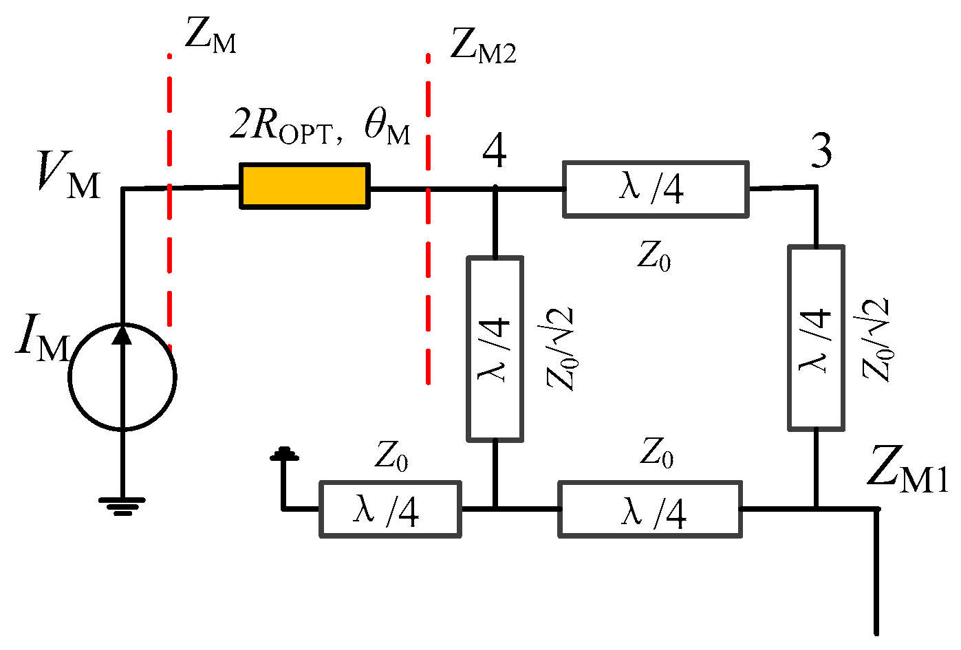
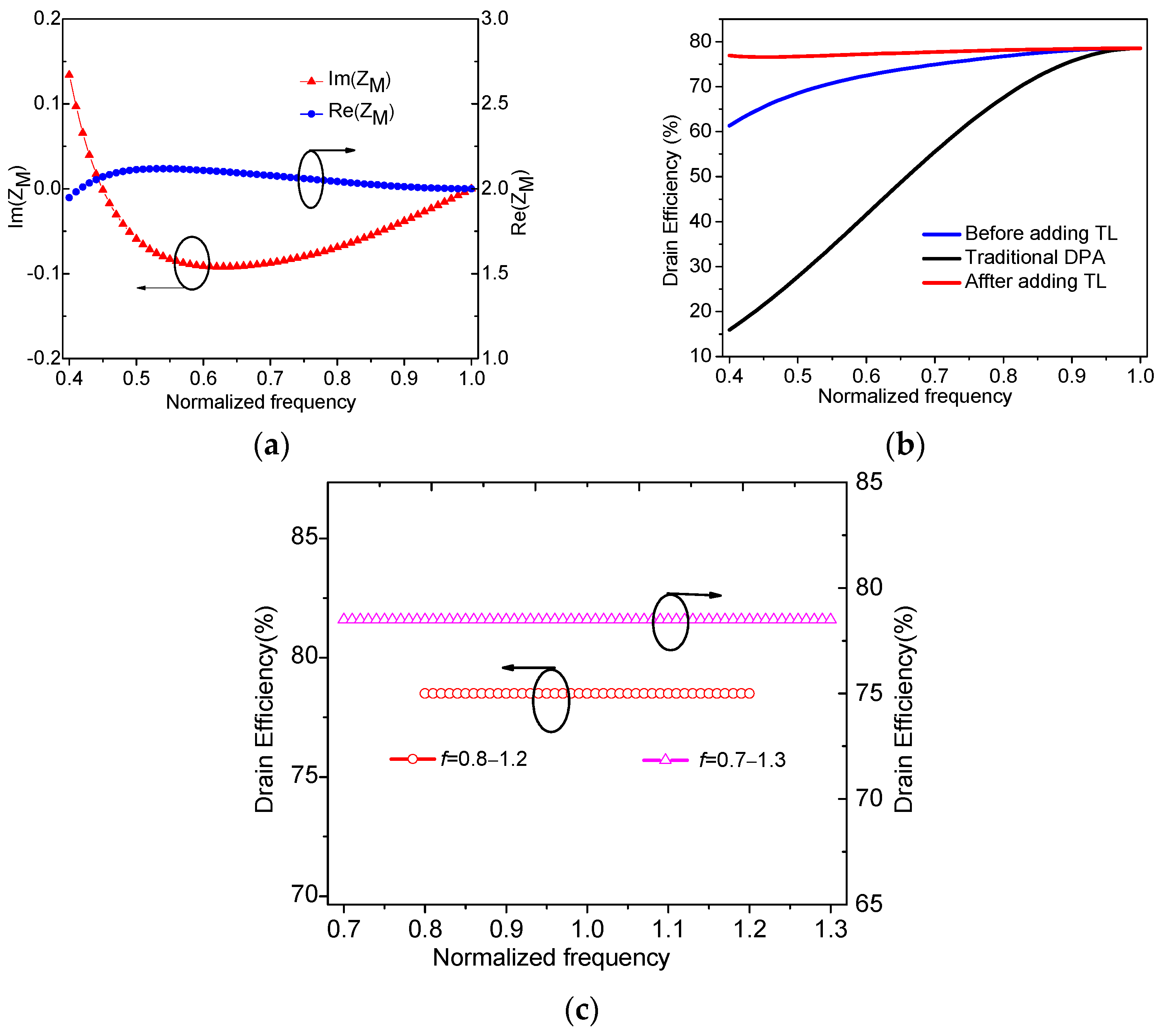
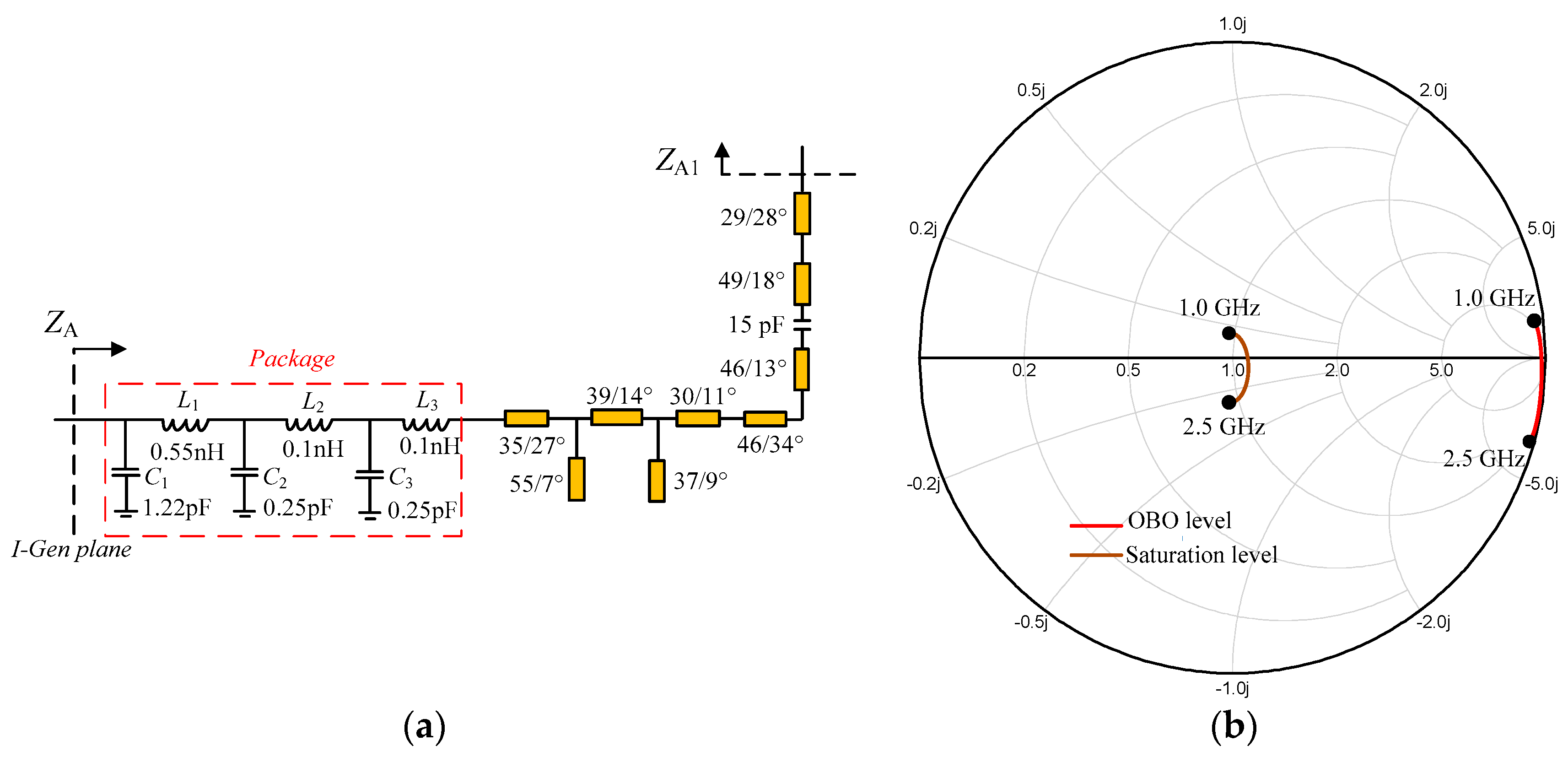
2.3. Improved Main PA Branch

As shown in Figure 6a, the drain efficiency of the proposed DPA is better than that of the traditional DPA. However, the drain efficiency can still drop to about 20% from the ideal drain efficiency. We now propose an improved main PA branch to further slow down the tendency of drain efficiency to decrease with normalized frequency. Figure 7 shows the topology of the improved main PA branch. Here a transmission line is inserted between the coupler and the drain of the transistor. Therefore, the impedance relationship between impedance ZM and ZM2 can be expressed as
Z M = 2 R OPT Z M 2 + j 2 R OPT tan θ M 2 R OPT + j Z M 2 tan θ M
where θ M = a r t a n I m Z M 2 / 2 .
Then, we can obtain the frequency characteristics of impedance ZM,OBO as shown in Figure 8a. Comparing Figure 8a with Figure 6b, it can be seen that the imaginary part of ZM,OBO in Figure 8a lies closer to zero. In addition, the corresponding drain efficiency at the OBO level is calculated in Figure 8b by using (18) and (19). As shown in Figure 8b, the drain efficiency of the improved main PA roughly maintains a constant profile across the normalized frequency band of 0.4–1. In addition, Figure 8c shows the drain efficiency of DPAs in [29,30], where the normalized frequency bands are 0.8–1.2, and 0.7–1.3 for [29,30], respectively. As shown in Figure 8b,c, the presented DPA has the ability to work in a lower normalized frequency band so as to have a larger relative bandwidth.
Based on the above analysis, the impedance transformation of the proposed DPA is displayed in Figure 9. As shown in Figure 9, at the saturation level, the load impedances of the main PA branch and the auxiliary PA branch are both Zload, and their values are complex. At the same time, the load impedances of the two PAs’ transistors are both ROPT. The impedance conversion situation is the same as that of a conventional DPA, except that the load impedance Zload of DPA is a complex impedance. At the OBO level, regarding the auxiliary PA branch, the impedance of this branch is finite and is defined as jXA, while the load impedance of the device is infinite. This impedance conversion is realized by employing the generalized transmission line. At the OBO level, regarding the main PA branch, the impedance of this branch is Zload in parallel with jXA, which is different from that of the traditional DPA due to the introduction of the finite impedance of the auxiliary PA branch, while the load impedance of the transistor is 2ROPT. This impedance conversion as required by the main PA is achieved by employing the modified coupler and the injected transmission line. The utilization of this modified coupler and the injected transmission line allows DPA operation with an acceptable efficiency into a lower normalized frequency band so as to achieve a larger relative bandwidth as compared to previous DPAs in the literature. Furthermore, the introduction of the finite load impedance of the auxiliary PA branch and the complex load impedance of the DPA effectively assists in meeting the impedance requirements required for the modified coupler deployment.
The parameters of the generalized transmission line in the auxiliary PA branch are easily obtained by using the following relationship:
Z A = Z A 2 Z A 1 + j Z A 2 tan θ A Z A 2 + j Z A 1 tan θ A
where ZA1 is equal to jXA and 2Zload at the OBO level and saturation level, respectively. Then, the calculated ZA2 and θA are expressed as
Z A 2 = X 2 + 1 + X X A
θ A = a r c t a n 2 X 2 + 1 + X X A X A
The corresponding parameter values are summarized in Table 2. We can use these parameters in Table 2 to design the DPA working in the normalized frequency range of 0.4–1.

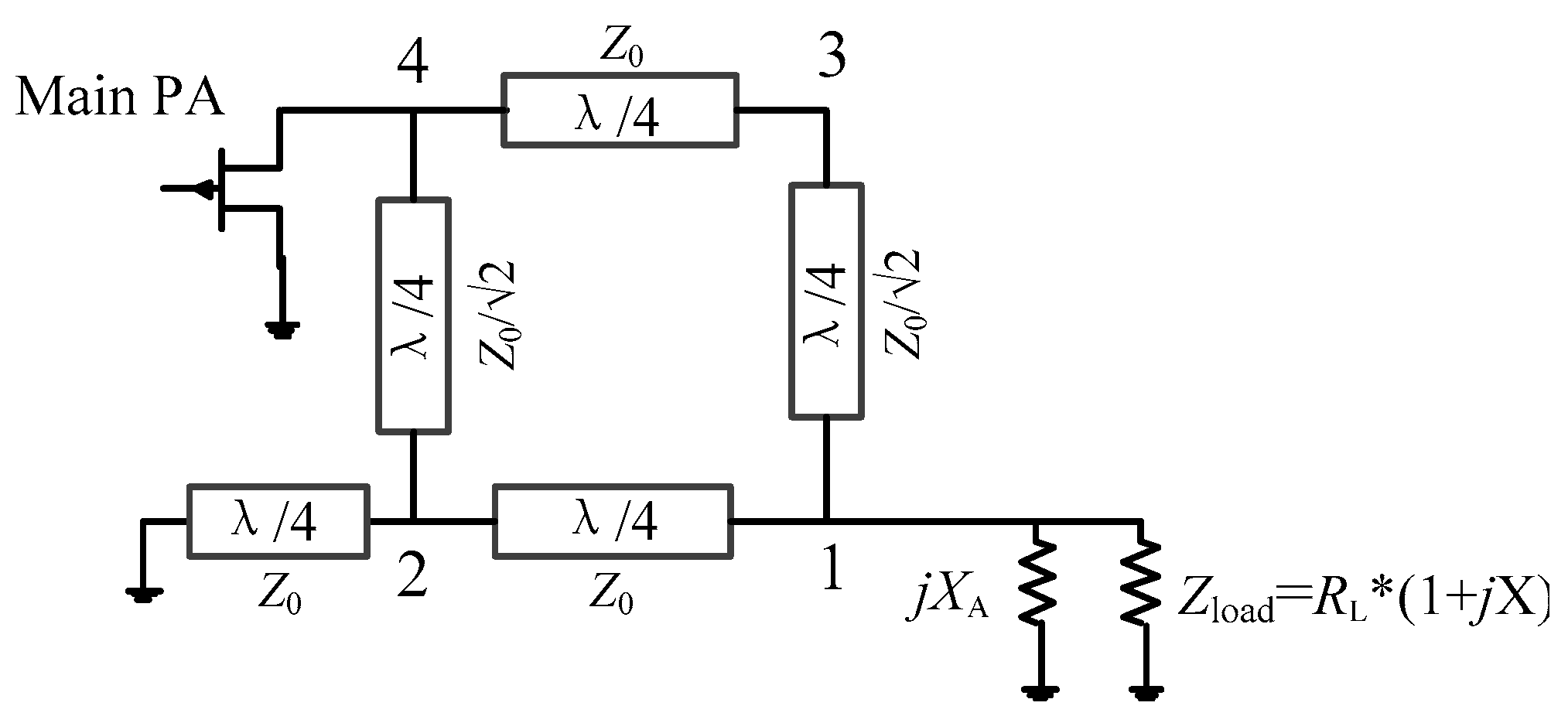
3. Design of The Proposed DPA

In this section, we present the complete design process for the enhanced bandwidth DPA based on the proposed load modulation network. In the previous section, the normalized frequency is used for analysis, and the normalized frequency band obtained is 0.4–1.0. Therefore, we can choose a different reference frequency in order to obtain actual working frequencies. In this paper, the reference frequency of 2.5 GHz is taken so that the actual working frequency range of 1–2.5 GHz can be achieved. This work focuses on the symmetrical DPA, so two CGH40010F transistors are employed to design the main PA and the auxiliary PA. The parameters of the transistors used can be obtained from the datasheet provided by the manufacturer. The designed circuits are based on Rogers R4350B substrate. The drain bias voltages of the main PA and auxiliary PA are both 28 V. The gate bias voltage of the main PA is −2.7 V, and that of the auxiliary PA is −5.8 V. For the selected transistor, the optimum load impedance ROPT is 32 Ω when considering Vknee.

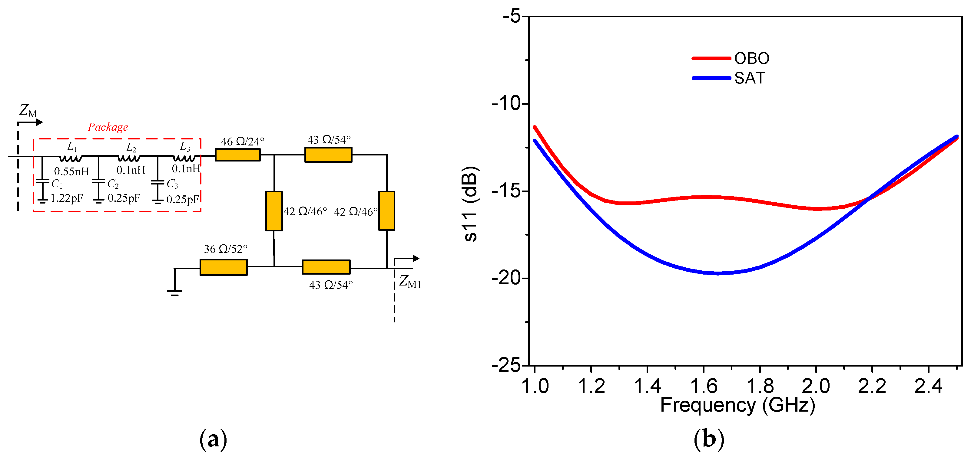
3.1. Output Networks

According to the description in Section 2, the output networks can be designed. Firstly, the output network of the main PA is designed based on the topology shown in Figure 7, where the phase θM varies from 46.7° to 0° in the frequency range of 1.0–2.5 GHz. In practical design, the package parameters of the transistor are considered [31] as part of the whole output network. Therefore, the injected transmission line and the modified coupler must adjust a little to meet the impedance requirements. The synthesized output circuit of the main PA is shown in Figure 10a. Figure 10b displays the simulated s11 of the designed output network under the condition of ZM1,OBO and ZM1,SAT. It can be seen that the simulated S11 is smaller than −10 dB across the frequency range of 1–2.5 GHz at both saturation and OBO levels, which validates that the designed output network is effective at realizing the impedance conversion well at different power levels within the target frequency band.
Next, the output network of auxiliary PA is designed by using the generalized transmission line obtained in Section 2. As per the analysis in Section 2, the characteristic impedance is changing from 1.52ROPT to ROPT over the target frequency range of 1–2.5 GHz, with the phase θA being between 85.4° and 90°. Similarly, the package parameters of the transistor are also included in the practical design. The complete output circuit including the package parameters is shown in Figure 11a. The simulated impedance ZA is displayed in Figure 11b. It can be seen that the simulated ZA is close to the open circuit at the OBO level and ROPT at the saturation level is matched, in 1.0–2.5 GHz. These realized impedance trajectories indicate the effectiveness of the output circuit of the auxiliary PA branch.

3.2. Post-Matching Network

In the previous analysis, the load impedance Zload is a complex impedance that is equal to 0.5ROPT(1 + jX). The value of X changes from 1.37 to 0 in the frequency range of 1.0–2.5 GHz. Therefore, a post-matching network is needed to transform this load impedance to 50 ohms. The complete matching network is synthesized as shown in Figure 12a,b; the simulated Zload is acceptable compared with the theoretical value of Zload.

3.3. Input Networks and Complete DPA

Firstly, an equal power divider is added to equally split the signal to the main PA and auxiliary PA. Here three stages are employed to meet bandwidth requirements. The input matching network is synthesized. Offset lines are also injected so that the signals of the two PA branches are combined in phase and transmitted to the load. Figure 13 shows the complete DPA with distributed parameters.
Figure 14 displays the simulated drain efficiency versus output power at several representative frequencies. As seen in Figure 14, the designed DPA can obtain over 43% drain efficiency at the 6 dB OBO level in the 1.0–2.5 GHz frequency range. At the same time, drain efficiency of over 62% can be obtained at the saturation level.
The impedance traces of ZM and ZA varying with power levels are plotted in Figure 15a,b at several representative frequencies. The load trajectories of ZM and ZA reveal that the designed DPA realizes the load modulation desired requirements across 1.0–2.5 GHz by using the proposed LMN structure.

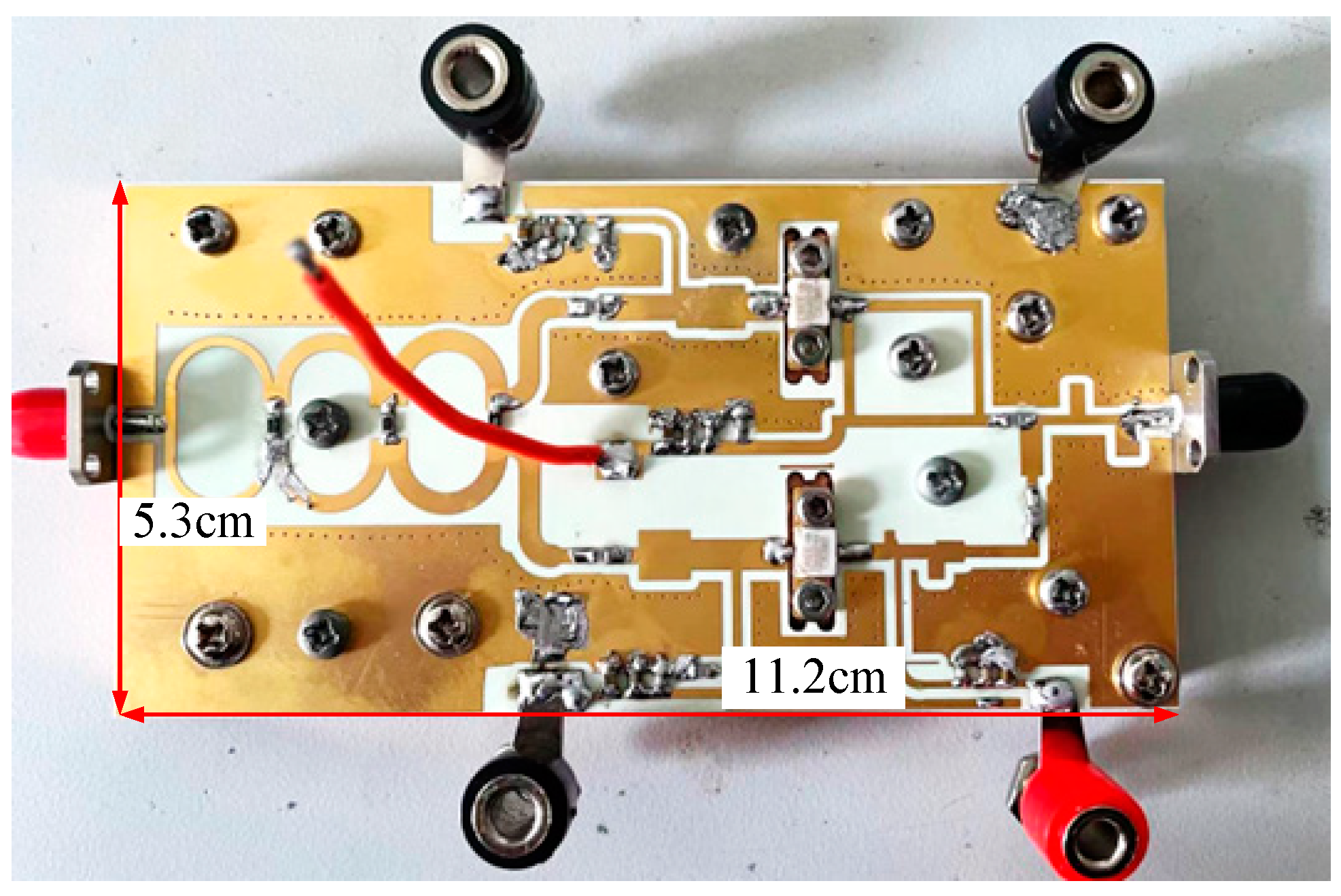
4. Experiment and Results Analysis

A DPA circuit was fabricated using Rogers 4350B (εr = 3.66, H = 20 mils) substrate based on the schematic shown in Figure 13. Figure 16 shows a photograph of the fabricated DPA. The overall size of the circuit is 11.2 cm × 5.3 cm.
The measured S-parameters are plotted in Figure 17. In the frequency range of 1.0–2.5 GHz, the measured s21 is 12.2–13.6 dB, and the measured s11 and s22 are smaller than −10 dB.

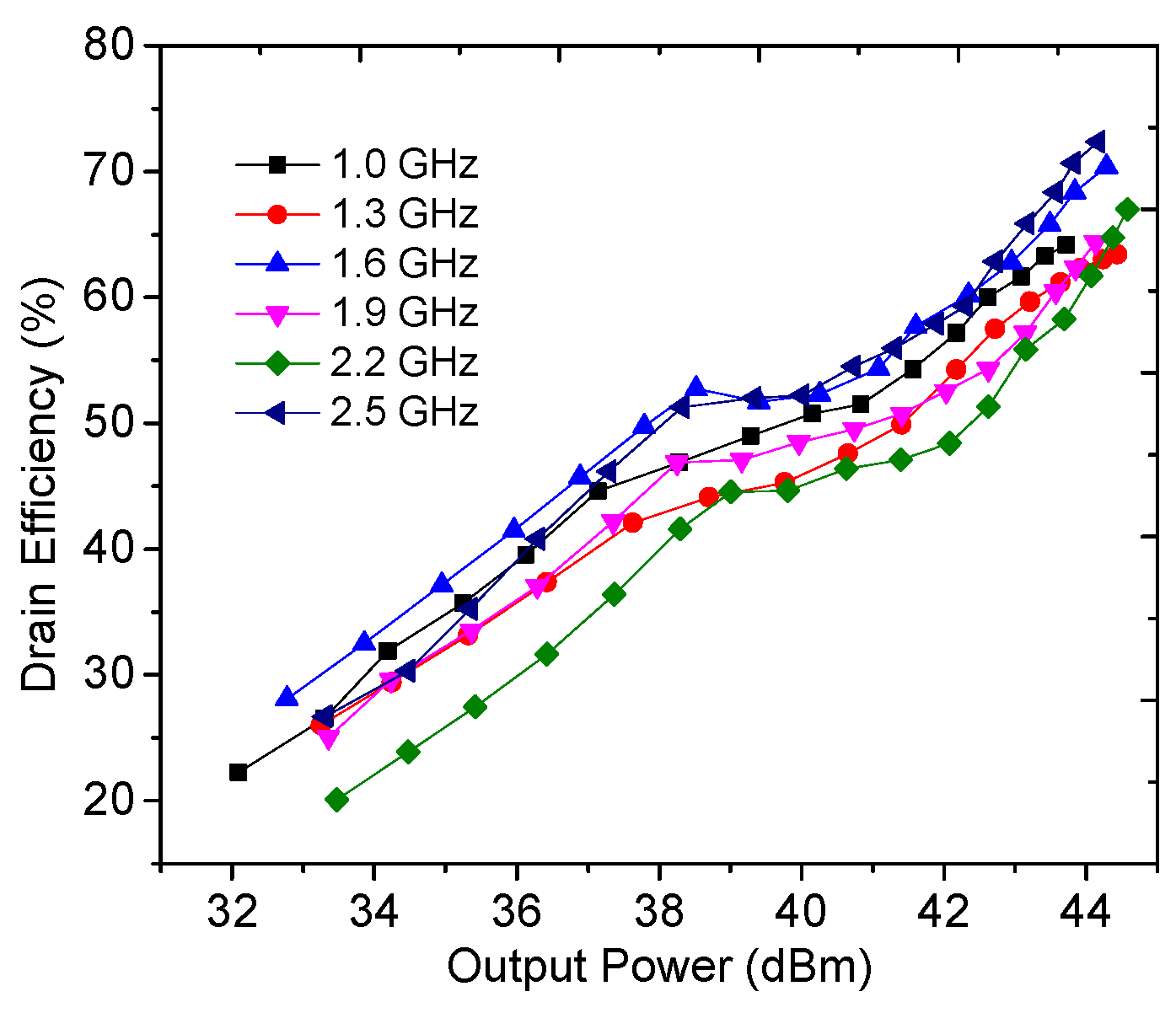
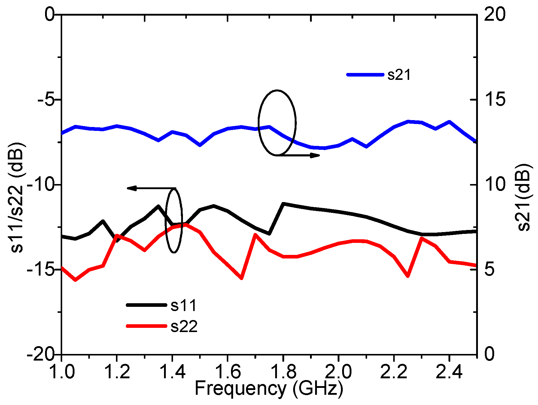
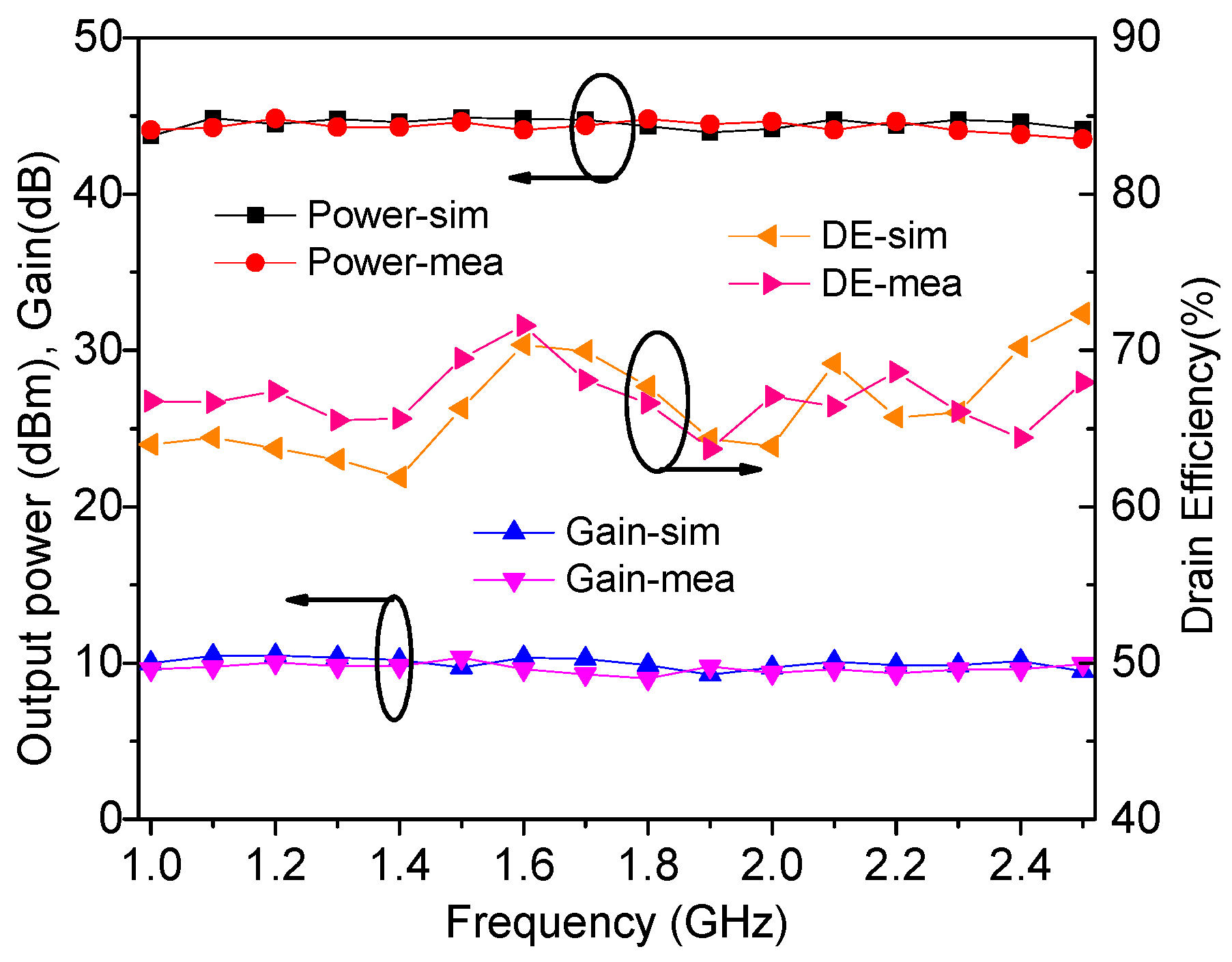
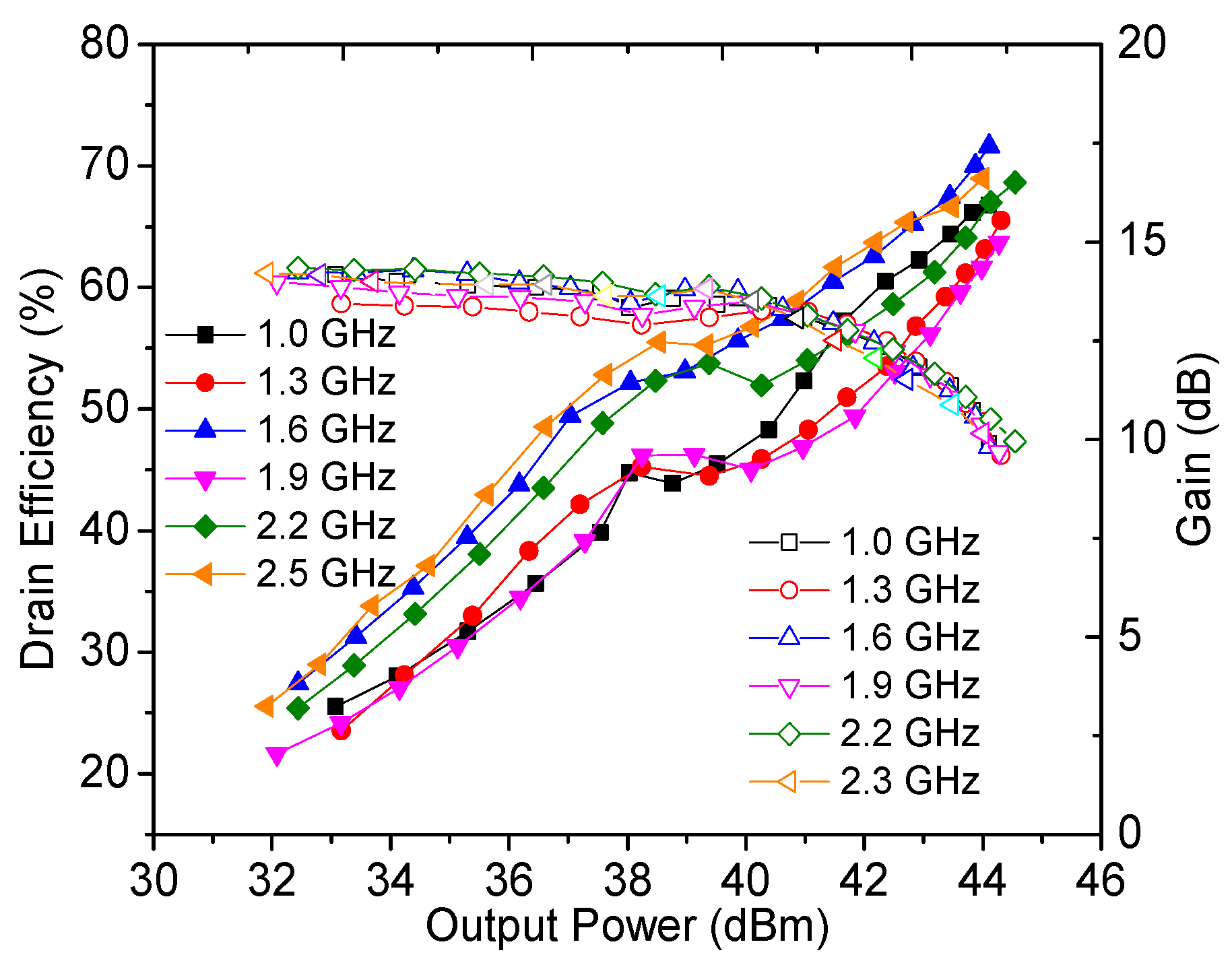
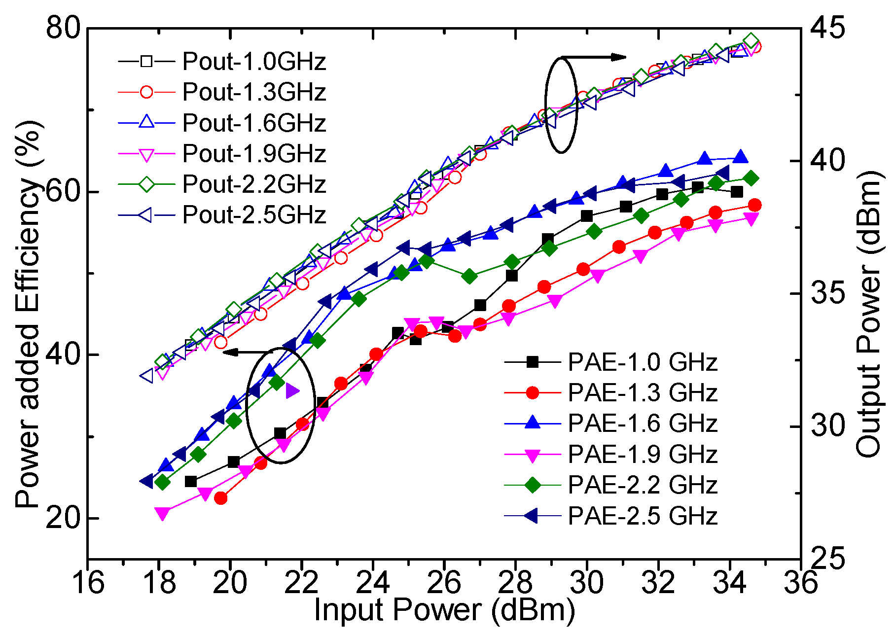
4.1. Continuous Wave Testing

The output power, drain efficiency, gain, and power-added efficiency were measured by using continuous wave signals and are plotted in Figure 18, Figure 19 and Figure 20. It can be seen from Figure 18 that an output power of 43.9–44.5 dBm with a drain efficiency of 63.7–71.6% can be obtained at the saturation level in 1.0–2.5 GHz, while the gain is between 9.6 dB and 10.3 dB. At the 6 dB OBO level, the realized drain efficiency is 45.2–53.7%. As shown in Figure 20, the power-added efficiency is between 42.3% and 64.1% within the dynamic load modulation range.
Table 3 lists several related and latest DPAs for comparison. It is obvious that the relative bandwidth of the proposed DPA is wider than that of the others except for that presented in [32], and the proposed DPA realizes similar performance, including in power, drain efficiency, and gain, when compared with the others.

4.2. LTE Testing at 40 MHz and 6.5 dB

To characterize the linearity of the designed DPA, the adjacent channel ratio (ACLR) was measured by employing an LTE signal with a bandwidth of 40 MHz and PAPR of 6.5 dB. The measured ACLR was obtained when an average output power of 37.6 dBm was produced, as displayed in Figure 21. As shown in Figure 21, the ACLR value is less than −30.2 dBc at 1.7 GHz, which is better than −49.5 dBc after adopting digital predistortion (DPD).

5. Conclusions

This paper proposes a novel load modulation network consisting of two transmission lines and a modified coupler. The utilization of this modified coupler makes the load modulation network work well in a lower normalized frequency band, resulting in a larger relative bandwidth compared with previously used networks. The corresponding parameters at each operation frequency are solved to realize DPAs with a relative bandwidth of 85.6%. For validation, a broadband DPA operating in 1.0–2.5 GHz was implemented based on the obtained parameter solutions. Measurements reveal that the implemented DPA can deliver an output power of over 43.9 dBm with drain efficiency above 63% at the saturation level in the frequency range of 1.0–2.5 GHz. The drain efficiency is above 45.3% at the 6 dB OBO level across the same frequency band. Compared with the previous works, this work is close to the state-of-the-art relative bandwidth performance.

Author Contributions

H.Z. and X.X. conceived and implemented the idea and wrote the paper; Z.Z. and C.G. reviewed and supervised the work. All authors have read and agreed to the published version of the manuscript.

Funding

This work was supported by the National Natural Science Foundation of China (Grant 62201181).

Institutional Review Board Statement

Not applicable.

Informed Consent Statement

Not applicable.

Data Availability Statement

Data are available on request from the authors.

Conflicts of Interest

The authors declare no conflict of interest.

References

  1. Nghiem, X.A.; Guan, J.; Hone, T.; Negra, R. Design of concurrent multiband Doherty power amplifiers for wireless applications. IEEE Trans. Microw. Theory Techn. 2013, 61, 4559–4568. [Google Scholar] [CrossRef]
  2. Huang, H.; Zhang, B.; Yu, C.; Gao, J.; Wu, Y.; Liu, Y. Design of Multioctave Bandwidth Power Amplifier Based on Resistive Second-Harmonic Impedance Continuous Class-F. IEEE Microw. Wirel. Compon. Lett. 2017, 27, 830–832. [Google Scholar] [CrossRef]
  3. Safari Mugisho, M.; Makarov, D.G.; Rassokhina, Y.V.; Grebennikov, A.; Thian, M. Generalized Class-E Power Amplifier with Shunt Capacitance and Shunt Filter. IEEE Trans. Microw. Theory Techn. 2019, 67, 3464–3474. [Google Scholar] [CrossRef] [Green Version]
  4. Li, Q.; He, S.; Shi, W.; Dai, Z.; Qi, T. Extend the class-B to class-J continuum mode by adding arbitrary harmonic voltage elements. IEEE Microw. Wireless Compon. Lett. 2016, 26, 522–524. [Google Scholar] [CrossRef]
  5. Zhou, X.Y.; Zheng, S.Y.; Chan, W.S.; Chen, S.; Ho, D. Broadband efficiency-enhanced mutually coupled harmonic post-matching Doherty power amplifier. IEEE Trans. Circuits Syst. I Reg. Pap. 2017, 64, 1758–1771. [Google Scholar] [CrossRef]
  6. Chang, H.C.; Hahn, Y.; Roblin, P.; Barton, T.W. New mixed mode design methodology for high-efficiency out-phasing chireix amplifiers. IEEE Trans. Circuits Syst. I Reg. Pap. 2019, 66, 1594–1607. [Google Scholar] [CrossRef]
  7. Collins, D.J.; Quaglia, R.; Powell, J.R.; Cripps, S.C. The Orthogonal LMBA: A Novel RFPA Architecture with Broadband Reconfigurability. IEEE Microw. Wirel. Compon. Lett. 2020, 30, 888–891. [Google Scholar] [CrossRef]
  8. Zhang, Z.; Cheng, Z.; Li, H. A Power Amplifier with Large High-Efficiency Range for 5G Communication. Sensors 2020, 20, 5581. [Google Scholar] [CrossRef]
  9. Bathich, K.; Markos, A.Z.; Boeck, G. Frequency response analysis and bandwidth extension of the Doherty amplifier. IEEE Trans. Microw. Theory Techn. 2011, 59, 934–944. [Google Scholar] [CrossRef]
  10. Giofre, R.; Piazzon, L.; Colantonio, P.; Giannini, F. A Doherty architecture with high feasibility and defined bandwidth behavior. IEEE Trans. Microw. Theory Techn. 2013, 61, 3308–3317. [Google Scholar] [CrossRef]
  11. Kang, D.; Kim, D.; Cho, Y.; Park, B.; Kim, J.; Kim, B. Design of bandwidth-enhanced Doherty power amplifiers for handset applications. IEEE Trans. Microw. Theory Techn. 2011, 59, 3474–3483. [Google Scholar] [CrossRef]
  12. Xia, J.; Yang, M.; Zhu, A. Improved Doherty amplifier design with minimum phase delay in output matching network for wideband application. IEEE Microw. Wirel. Compon. Lett. 2016, 26, 52–54. [Google Scholar] [CrossRef] [Green Version]
  13. Rubio, J.M.; Fang, J.; Camarchia, V.; Quaglia, R.; Pirola, M.; Ghione, G. 6-GHz wideband GaN Doherty power amplifier exploiting output compensation stages. IEEE Trans. Microw. Theory Techn. 2012, 60, 2543–2548. [Google Scholar] [CrossRef] [Green Version]
  14. Xia, J.; Yang, M.; Guo, Y.; Zhu, A. A broadband high-efficiency Doherty power amplifier with integrated compensating reactance. IEEE Trans. Microw. Theory Techn. 2016, 64, 2014–2024. [Google Scholar] [CrossRef] [Green Version]
  15. Xia, J.; Chen, W.; Meng, F.; Yu, C.; Zhu, X. Improved three stage Doherty amplifier design with impedance compensation in load combiner for broadband applications. IEEE Trans. Microw. Theory Techn. 2019, 67, 778–786. [Google Scholar] [CrossRef]
  16. Fang, X.-H.; Liu, H.-Y.; Cheng, K.-K.-M.; Boumaiza, S. Modified Doherty amplifier with extended bandwidth and back-off power range using optimized auxiliary combining current ratio. IEEE Trans. Microw. Theory Techn. 2018, 66, 5347–5357. [Google Scholar] [CrossRef]
  17. Yang, Z.; Yao, Y.; Li, M.; Jin, Y.; Li, T.; Dai, Z.; Tang, F.; Li, Z. Bandwidth extension of Doherty power amplifier using complex combining load with noninfinity auxiliarying impedance. IEEE Trans. Microw. Theory Techn. 2019, 67, 765–777. [Google Scholar] [CrossRef]
  18. Pang, J.; He, S.; Huang, C.; Dai, Z.; Peng, J.; You, F. A post matching Doherty power amplifier employing low-order impedance inverters for broadband applications. IEEE Trans. Microw. Theory Techn. 2015, 63, 4061–4071. [Google Scholar] [CrossRef]
  19. Zhou, X.Y.; Zheng, S.Y.; Chan, W.S.; Fang, X.; Ho, D. Postmatching Doherty power amplifier with extended back-off range based on selfgenerated harmonic injection. IEEE Trans. Microw. Theory Techn. 2018, 66, 1951–1963. [Google Scholar] [CrossRef]
  20. Pang, J.; He, S.; Dai, Z.; Huang, C.; Peng, J.; You, F. Design of a post matching asymmetric Doherty power amplifier for broadband applications. IEEE Microw. Wireless Compon. Lett. 2016, 26, 52–54. [Google Scholar] [CrossRef]
  21. Kang, H.; Lee, H.; Lee, W.; Oh, H.; Lim, W.; Koo, H.; Park, C.; Hwang, K.C.; Lee, K.-Y.; Yang, Y. Octave bandwidth Doherty power amplifier using multiple resonance circuit for the auxiliarying amplifier. IEEE Trans. Circuits Syst. I Reg. Pap. 2019, 66, 583–593. [Google Scholar] [CrossRef]
  22. Shi, W.; He, S.; Zhu, X.; Song, B.; Zhu, Z.; Naah, G.; Zhang, M. Broadband continuous-mode Doherty power amplifiers with noninfinity auxiliarying impedance. IEEE Trans. Microw. Theory Techn. 2018, 66, 1034–1046. [Google Scholar] [CrossRef]
  23. Huang, C.; He, S.; You, F. Design of broadband modified class-J Doherty power amplifier with specific second harmonic terminations. IEEE Access 2018, 6, 2531–2540. [Google Scholar] [CrossRef]
  24. Zhang, Z.; Cheng, Z.; Li, H.; Ke, H.; Guo, Y.J. A Broadband Doherty Power Amplifier with Hybrid Class-EFJ Mode. IEEE Trans. Circuits Syst. I Reg. Papers. 2020, 67, 4270–4280. [Google Scholar] [CrossRef]
  25. Wu, D.Y.-T.; Boumaiza, S. A modified Doherty configuration for broadband amplification using symmetrical devices. IEEE Trans. Microw. Theory Techn. 2012, 60, 3201–3213. [Google Scholar] [CrossRef]
  26. Gustafsson, D.; Andersson, C.M.; Fager, C. A modified Doherty power amplifier with extended bandwidth and reconfigurable efficiency. IEEE Trans. Microw. Theory Techn. 2013, 61, 533–542. [Google Scholar] [CrossRef]
  27. Giofre, R.; Piazzon, L.; Colantonio, P.; Giannini, F. An ultrabroadband GaN Doherty amplifier with 83% of fractional bandwidth. IEEE Microw. Wirel. Compon. Lett. 2014, 24, 775–777. [Google Scholar] [CrossRef]
  28. Jundi, A.; Boumaiza, S. A series-connected-load Doherty power amplifier with push–pull main and auxiliary amplifiers for base station applications. IEEE Trans. Microw. Theory Techn. 2020, 68, 796–807. [Google Scholar] [CrossRef]
  29. Li, M.; Pang, J.; Li, Y.; Zhu, A. Bandwidth Enhancement of Doherty Power Amplifier Using Modified Load Modulation Network. IEEE Trans. Circuits Syst. I Reg. Papers. 2020, 67, 1824–1834. [Google Scholar] [CrossRef]
  30. Xu, Y.; Pang, J.; Wang, X.; Zhu, A. Enhancing Bandwidth and Back-Off Range of Doherty Power Amplifier with Modified Load Modulation Network. IEEE Trans. Microw. Theory Techn. 2021, 69, 2291–2303. [Google Scholar] [CrossRef]
  31. Zhang, Z.; Cheng, Z.; Ke, H.; Liu, G. A Broadband High-Efficiency Power Amplifier by Using Branch Line Coupler. IEEE Microw. Wirel. Compon. Lett. 2020, 30, 880–883. [Google Scholar] [CrossRef]
  32. Moreno Rubio, J.J.; Camarchia, V.; Pirola, M.; Quaglia, R. Design of an 87% fractional bandwidth Doherty power amplifier supported by a simplified bandwidth estimation method. IEEE Trans. Microw. Theory Techn. 2018, 66, 1319–1327. [Google Scholar] [CrossRef] [Green Version]
  33. Naah, G.; Giofrè, R. Empowering the Bandwidth of Continuous mode Symmetrical Doherty Amplifiers by Leveraging on Fuzzy Logic Techniques. IEEE Trans. Microw. Theory Techn. Techn. 2019, 68, 3134–3147. [Google Scholar] [CrossRef] [Green Version]
  34. Liu, H.-Y.; Fang, X.-H.; Cheng, K.-K.-M. Bandwidth enhancement of frequency dispersive Doherty power amplifier. IEEE Microw. Wirel. Compon. Lett. 2020, 30, 185–188. [Google Scholar] [CrossRef]
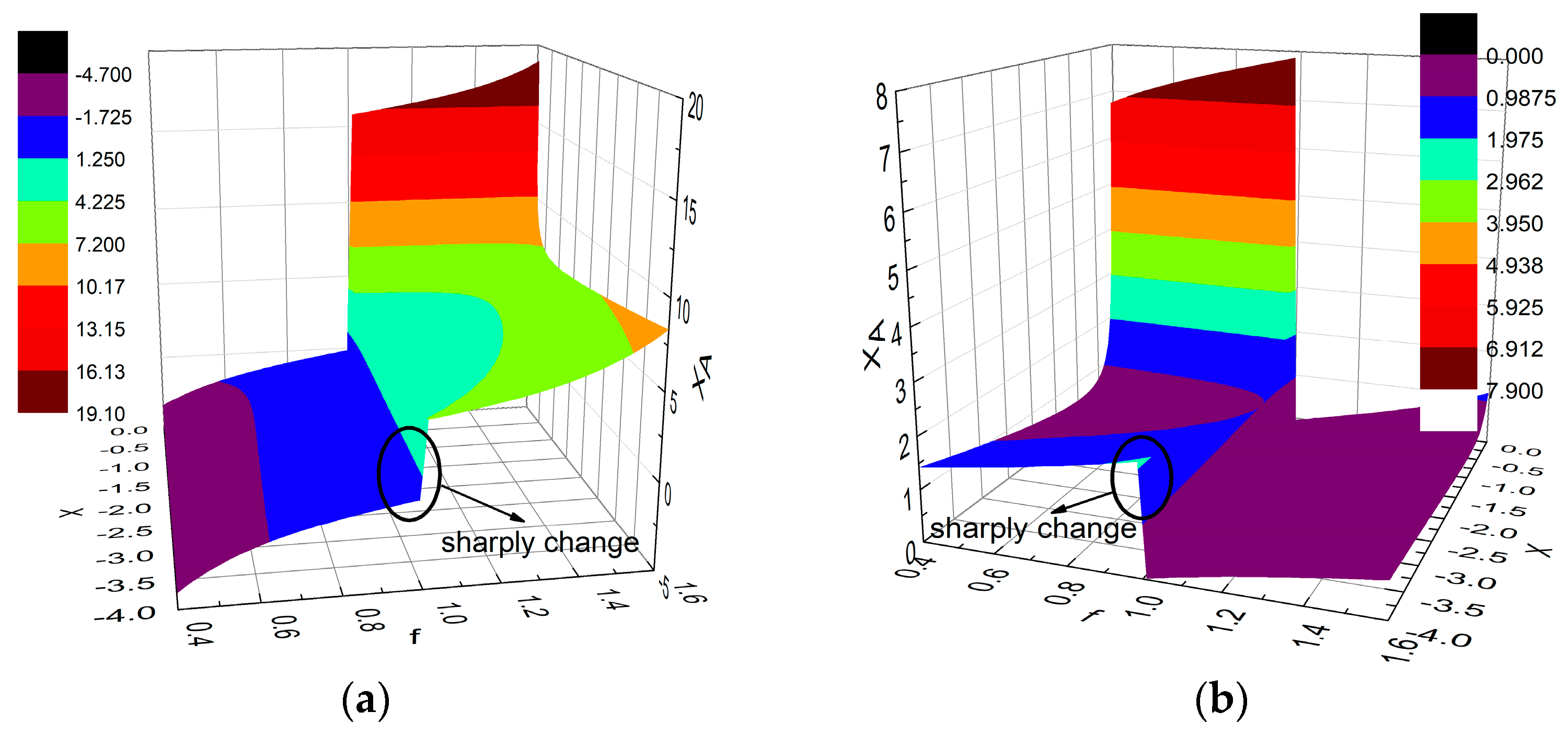
Figure 1. Conventional DPA topology.
Sensors 23 02767 g001
Figure 2. (a) Proposed DPA topology; (b) modified coupler.
Sensors 23 02767 g002
Figure 3. Equivalent schematic diagram of the main PA branch at the OBO level.
Sensors 23 02767 g003
Figure 4. Relationships between XA, X, and f: (a) relationship expressed by (11); (b) relationship expressed by (12).
Sensors 23 02767 g004
Figure 5. Equivalent schematic diagram of the main PA branch at the saturation level.
Sensors 23 02767 g005
Figure 6. Drain efficiency and impedance versus the normalized frequency: (a) drain efficiency versus the normalized frequency; (b) impedance ZM versus the normalized frequency.
Sensors 23 02767 g006
Figure 7. Improved main PA branch.
Sensors 23 02767 g007
Figure 8. Frequency characteristics: (a) impedance ZM,OBO; (b) theoretical drain efficiency in this work; (c) theoretical drain efficiency of DPAs in [29,30].
Sensors 23 02767 g008
Figure 9. Impedance transformation of the proposed DPA.
Sensors 23 02767 g009
Figure 10. Main PA branch: (a) output network of the main PA; (b) simulated s11.
Sensors 23 02767 g010
Figure 11. Auxiliary PA branch: (a) designed output network; (b) simulated ZA.
Sensors 23 02767 g011
Figure 12. (a) Post-matching network; (b) simulated impedance Zload (normalized ROPT).
Sensors 23 02767 g012
Figure 13. Completed DPA circuit with distributed parameters.
Sensors 23 02767 g013
Figure 14. Simulated drain efficiency versus output power.
Sensors 23 02767 g014
Figure 15. Trajectories of impedance ZM and ZA at several representative frequencies: (a) impedance ZM; (b) impedance ZA.
Sensors 23 02767 g015
Figure 16. Photograph of the designed DPA.
Sensors 23 02767 g016
Figure 17. Measured s11, s22, and s21 of the designed DPA.
Sensors 23 02767 g017
Figure 18. Simulated and measured performance at the saturation level.
Sensors 23 02767 g018
Figure 19. Measured drain efficiency and gain versus output power.
Sensors 23 02767 g019
Figure 20. Measured power-added efficiency and output power versus input power.
Sensors 23 02767 g020
Figure 21. Measured ACLR at 1.7 GHz.
Sensors 23 02767 g021
Table 1. The values of X and XA at representative frequencies.
ValueXXA1XA2
f = 0.41.37−0.50−3.37
f = 0.51−0.40−2.62
f = 0.60.72−0.34−2.15
f = 0.70.51−0.30−1.93
f = 0.80.32−0.25−2.09
f = 0.90.16−0.15−3.40
f = 1.000
XA1 refers to the first solution of XA; XA2 refers to the second solution of XA.
Table 2. The values of the corresponding parameters.
Parameterf = 0.4f = 0.5f = 0.6f = 0.7f = 0.8f = 0.9f = 1.0
X1.3710.720.510.320.150
θM (°)46.737.430.123.717.08.90
XA−0.42−0.38−0.35−0.33−0.26−0.150
ZA21.521.271.121.041.001.001.00
θA (°)85.985.785.485.586.287.690
Table 3. Several related and latest broadband DPAs.
Ref.Freq (B.W.)
(GHz)
Pout@SAT
(dBm)
DE@SAT (%)DE@ 6 dB
OBO (%)
Device
[17]1.1–2.4 (74%)43.3–45.455–6843.8–54.92 × 13 W GaN
[22]1.6–2.7 (51%)43.8–45.256–75.346.5–63.52 × 13 W GaN
[23]3.3–3.75 (13%)48–48.558–7147–592 × 16 W GaN
[24]1.2–2.8 (78%)43.7–44.160.5–74.248.1–57.62 × 13 W GaN
[27]1.0–2.5 (83%)40–4245–8335–582 × 8 W GaN
[29]2.8–3.55 (24%)43–4566–7842–532 × 13 W GaN
[32]1.5–3.8 (87%)42.3–43.442–6333–552 × 13 W GaN
[33]1.2–2.4 (67%)42–4541.6–8135–632 × 13 W GaN
[34]1.4–2.55 (58%)41.9–42.262–7448–582 × 8 W GaN
This work1.0–2.5 (85.6%)43.9–44.563.7–71.645.2–53.72 × 13 W GaN
Disclaimer/Publisher’s Note: The statements, opinions and data contained in all publications are solely those of the individual author(s) and contributor(s) and not of MDPI and/or the editor(s). MDPI and/or the editor(s) disclaim responsibility for any injury to people or property resulting from any ideas, methods, instructions or products referred to in the content.

