
Compact Ultra-Wideband Wilkinson Power Divider in Parallel Stripline with Modified Isolation Branches

Abstract
:1. Introduction
2. Design of a Three-Stage Power Divider in a Parallel Stripline
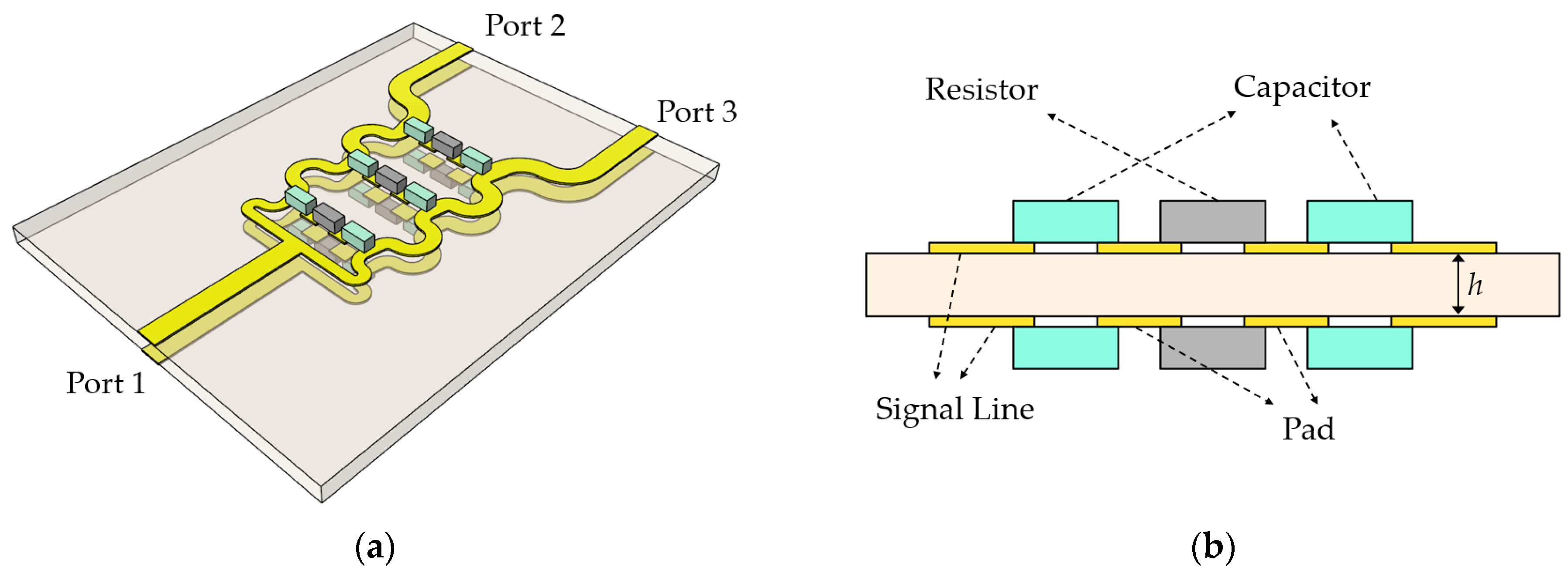
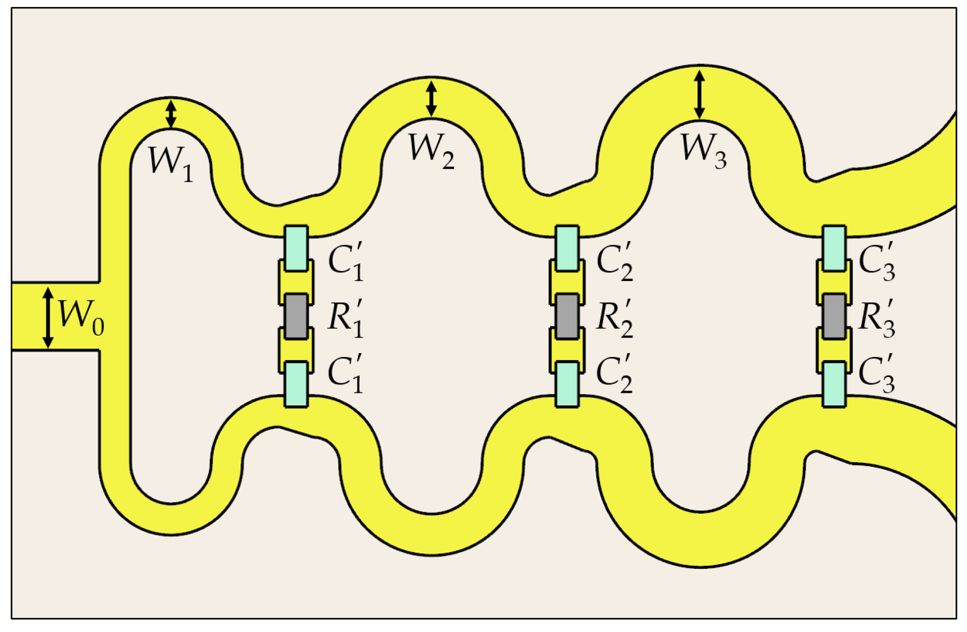
2.1. Configuration
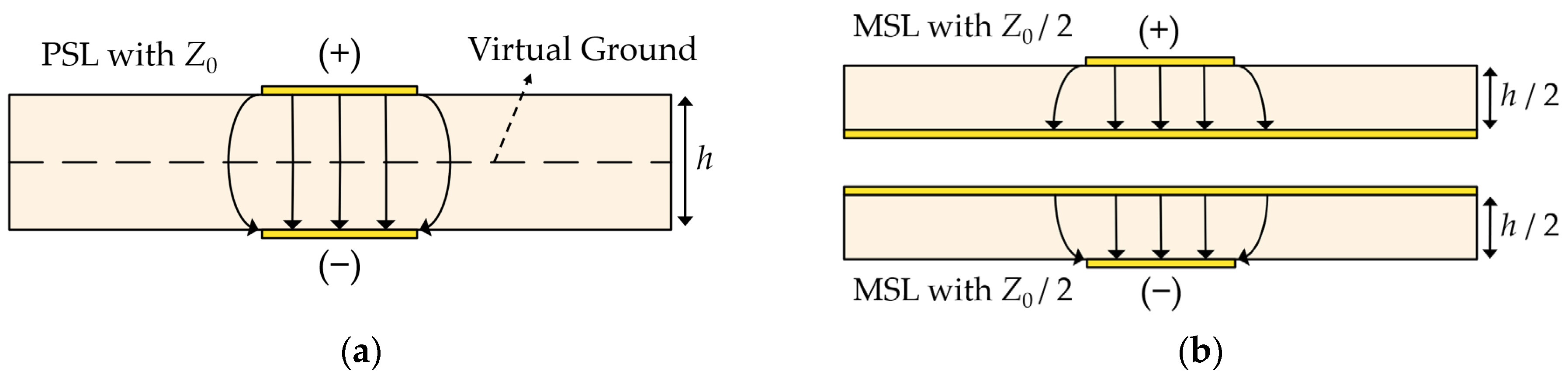
2.2. Analysis
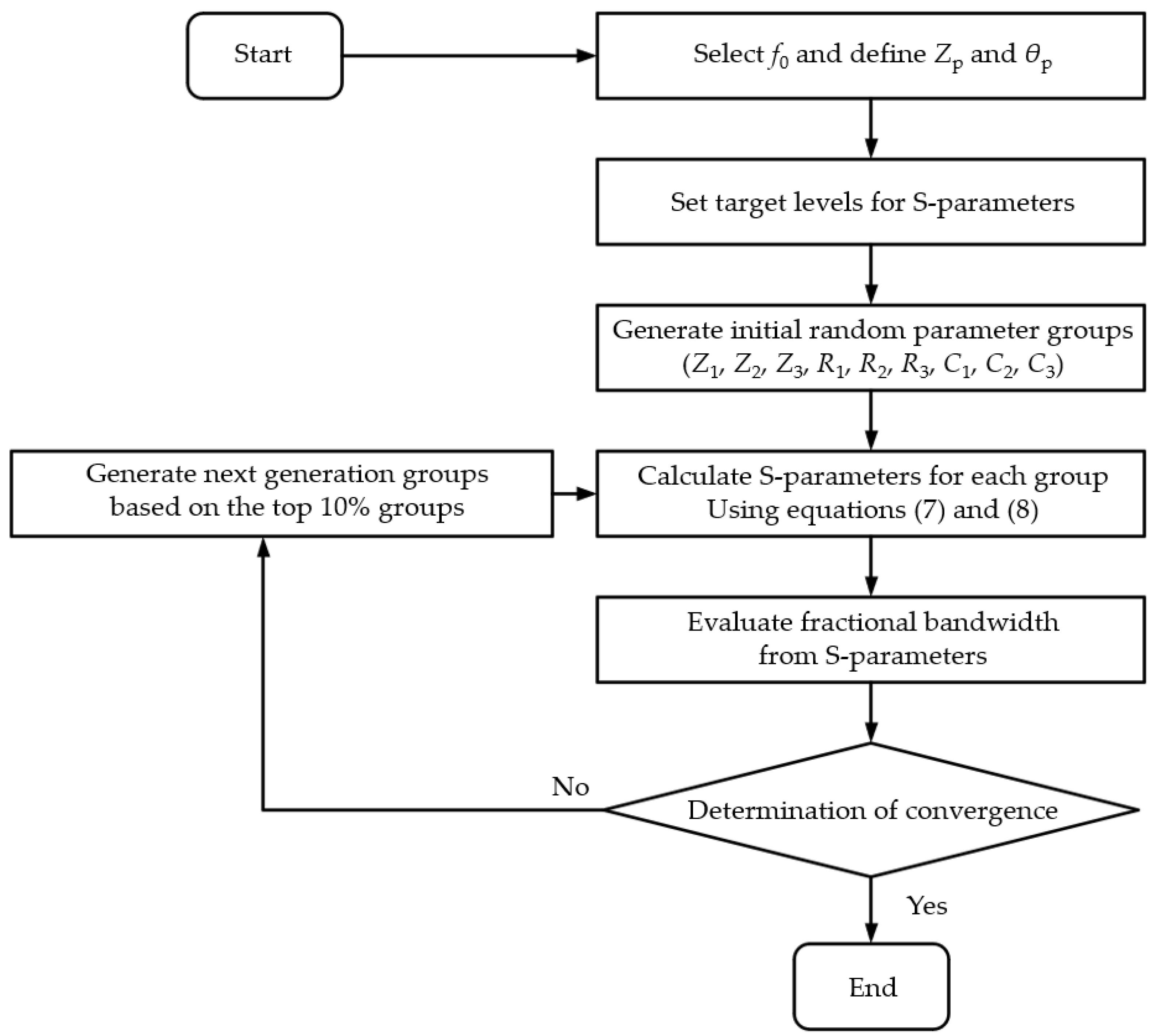
2.3. Optimization Algorithm
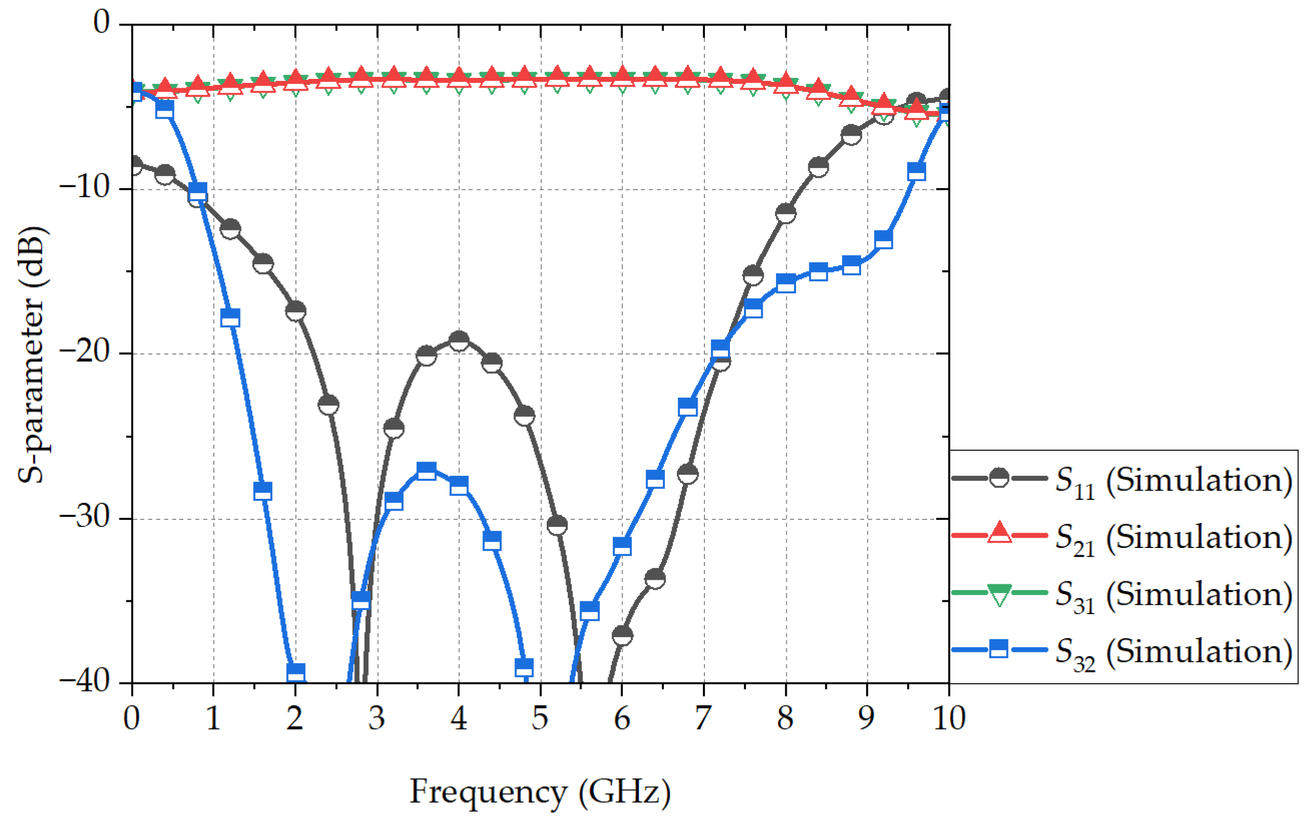
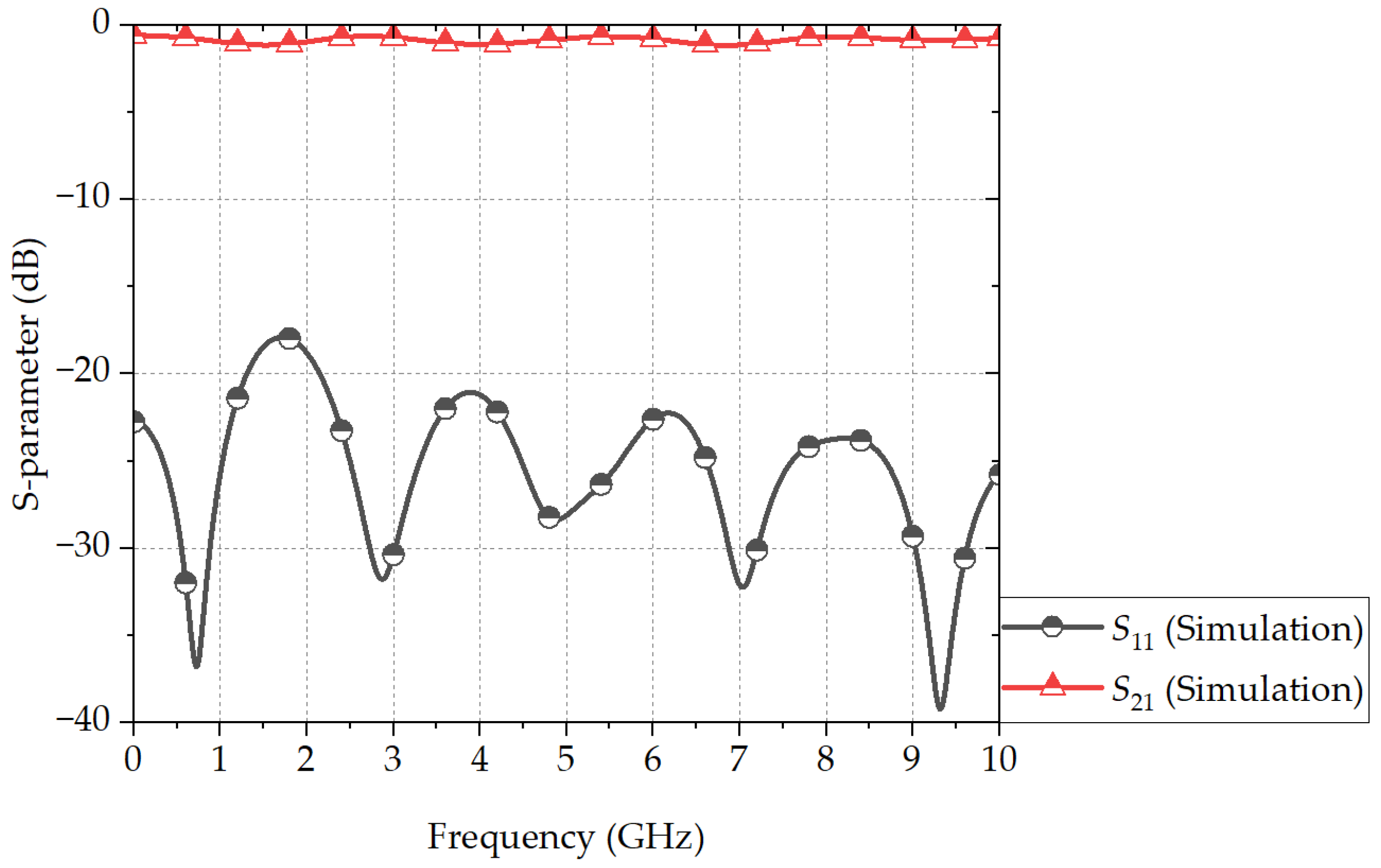
3. Simulations
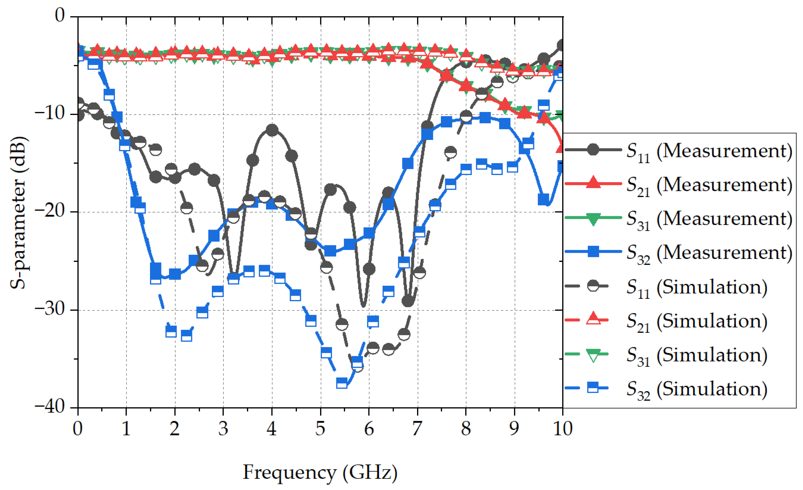
4. Fabrication and Measurements
5. Conclusions
Author Contributions
Funding
Institutional Review Board Statement
Informed Consent Statement
Data Availability Statement
Conflicts of Interest
References
- Martin, F.; Zhu, L.; Medina, F.; Hong, J.S. Balanced Microwave Filters; John Wiley & Sons: Hoboken, NJ, USA, 2018. [Google Scholar]
- Choi, J.S.; Min, B.C.; Kim, M.J.; Kumar, S.; Choi, H.C.; Kim, K.W. Design of a Common-Mode Rejection Filter Using Dumbbell-Shaped Defected Ground Structures Based on Equivalent Circuit Models. Electronics 2023, 12, 3230. [Google Scholar] [CrossRef]
- Testa, P.V.; Carta, C.; Barahona, M.; Ellinger, F. 0.5–20-GHz UWB Distributed Combiners and Dividers for Multi-Antenna Transceivers. IEEE Trans. Microw. Theory Tech. 2017, 65, 3087–3098. [Google Scholar] [CrossRef]
- Min, B.C.; Lee, G.H.; Lee, J.S.; Nashuha, S.H.; Choi, H.C.; Kim, K.W. Ultra-Wideband Differential Line-to-Balanced Line Transitions for Super-High-Speed Digital Transmission. Sensors 2022, 22, 6873. [Google Scholar] [CrossRef]
- Chang, C.; Fang, R.; Wang, C. Bended Differential Transmission Line Using Compensation Inductance for Common-Mode Noise Suppression. IEEE Trans. Compon. Packag. Manuf. Technol. 2012, 2, 1518–1525. [Google Scholar] [CrossRef]
- Shiue, G.-H.; Guo, W.-D.; Lin, C.-M.; Wu, R.-B. Noise reduction using compensation capacitance for bend discontinuities of differential transmission lines. IEEE Trans. Adv. Packag. 2006, 29, 560–569. [Google Scholar] [CrossRef]
- Wong, S.W.; Zhu, L. Ultra-Wideband Power Divider with Good In-Band Splitting and Isolation Performances. IEEE Microw. Wirel. Compon. Lett. 2008, 18, 518–520. [Google Scholar] [CrossRef]
- Liu, Y.; Zhu, L.; Sun, S. Proposal and Design of Power Divider with Wideband Power Division and Port-to-Port Isolation: A New Topology. IEEE Trans. Microw. Theory Tech. 2020, 68, 1431–1438. [Google Scholar] [CrossRef]
- Zhang, W.; Ma, Z.; Liu, F.; Ohira, M. A novel compact wideband microstrip Wilkinson power divider. IEICE Electron. Express. 2021, 18, 20210308. [Google Scholar] [CrossRef]
- Okada, Y.; Kawai, T.; Enokihara, A. Wideband Lumped-Element Wilkinson Power Divider Using LC-Ladder Circuits. In Proceedings of the 2015 European Microwave Conference, Paris, France, 7–10 September 2015. [Google Scholar]
- Cohn, S.B. A Class of Broadband Three-Port TEM-Mode Hybrids. IEEE Trans. Microw. Theory Tech. 1968, 16, 110–116. [Google Scholar] [CrossRef]
- Lee, S.W.; Kim, C.S.; Choi, K.S.; Park, J.S.; Ahn, D. A General Design Formula of Multi-Section Power Divider Based on Singly Terminated Filter Design Theory. In Proceedings of the 2001 IEEE MTT-S International Microwave Symposium Digest, Phoenix, AZ, USA, 20–24 May 2001. [Google Scholar]
- Ekinge, R.B. A New Method of Synthesizing Matched Broad-Band TEM-Mode Three-ports. IEEE Trans. Microw. Theory Tech. 1971, 19, 81–88. [Google Scholar] [CrossRef]
- Chiu, L.; Yum, T.Y.; Xue, Q.; Chan, C.H. A Wideband Compact Parallel-Strip 180° Wilkinson Power Divider for Push-Pull Circuitries. IEEE Microw. Wirel. Compon. Lett. 2006, 16, 49–51. [Google Scholar] [CrossRef]
- Yoon, Y.C.; Kim, Y. Miniaturized Multi-Section Power Divider with Parallel RC Isolation Circuit. J. Electromagn. Eng. Sci. 2019, 19, 147–152. [Google Scholar] [CrossRef]
- Yu, T. A Broadband Wilkinson Power Divider Based on the Segmented Structure. IEEE Trans. Microw. Theory Tech. 2018, 66, 1902–1911. [Google Scholar] [CrossRef]
- Nor, M.Z.B.M.; Rahim, S.K.A.; Sabran, M.I.B.; Rani, M.S.B.A. Wideband Planar Wilkinson Power Divider Using Double-Sided Parallel-Strip Line Technique. Prog. Electromagn. Res. 2013, 36, 181–193. [Google Scholar] [CrossRef]
- Chiu, L.; Xue, Q. A Parallel-Strip Ring Power Divider with High Isolation and Arbitrary Power-Dividing Ratio. IEEE Trans. Microw. Theory Tech. 2007, 55, 2419–2426. [Google Scholar] [CrossRef]
- Kim, S.G.; Chang, K. Ultrawide-Band Transitions and New Microwave Components Using Double-Sided Parallel-Strip Lines. IEEE Trans. Microw. Theory Tech. 2004, 52, 2148–2152. [Google Scholar] [CrossRef]
- Lee, G.H.; Kim, K.W.; Choi, H.C. Development of Ultra-Wideband Microstrip-to-Parallel Stripline Transition Based on Conformal Mapping. J. Korean Inst. Electromagn. Eng. Sci. 2020, 31, 216–224. [Google Scholar] [CrossRef]


| 43.7 Ω | 36.0 Ω | 29.2 Ω | 43.1 Ω | 114.9 Ω | 184.6 Ω | 3.34 pF | 3.70 pF | 1.71 pF |
| 1.52 mm | 0.70 mm | 0.93 mm | 1.24 mm | 43 Ω | 110 Ω | 180 Ω | 3.3 pF | 3.7 pF | 1.7 pF |
| Reference | Topology | Center Frequency (GHz) | Insertion Loss (dB) | Return Loss (dB) | Isolation (dB) | Fractional Bandwidth | Total Electrical Length (°) 2 |
|---|---|---|---|---|---|---|---|
| [7] | MSL WPD * with coupled line | 6.8 | 0.4 @ 6.8 GHz | 10 | 10 | 97.1% | 180 |
| [8] | MSL WPD with coupled line | 2.5 | 0.7 | 10 | 17.5 | 78% | 270 |
| [9] | MSL WPD with ring structure | 3 | 0.8 (max) | 10 | 10 | 100% | 101.25 |
| [10] | MSL WPD with artificial transmission line | 0.125 0.3 | - | 17 | 18 | 100% 102.5% | - |
| [11] | Three-stage conventional WPD 1 | 3.84 | 0.1 (max) | 18 | 18 | 126% | 270 |
| [15] | Three-stage MSL WPD with parallel RC isolation branches | 2 | 0.2 | 15 | 15 | 117% | 179 |
| [16] | Three-stage MSL WPD with RC isolation branches and DGS | 0.5 | 0.47 @ 0.5 GHz | 18 | 18 | 108% | 90 |
| [17] | Three-stage PSL WPD | 4 | 1.3 (max) | 10 | 10 | 100% | - |
| [18] | PSL ring power divider | 2 | 0.7 (max) | 10 | 25 | 96.5% | 180 |
| This work | Three-stage PSL WPD with series RC isolation branches | 3.84 | 1.4 (max) | 10 | 18 | 139.5% | 207 |
Disclaimer/Publisher’s Note: The statements, opinions and data contained in all publications are solely those of the individual author(s) and contributor(s) and not of MDPI and/or the editor(s). MDPI and/or the editor(s) disclaim responsibility for any injury to people or property resulting from any ideas, methods, instructions or products referred to in the content. |
© 2024 by the authors. Licensee MDPI, Basel, Switzerland. This article is an open access article distributed under the terms and conditions of the Creative Commons Attribution (CC BY) license (https://creativecommons.org/licenses/by/4.0/).
Share and Cite
Go, D.-J.; Min, B.-C.; Kim, M.-J.; Choi, H.-C.; Kim, K.-W. Compact Ultra-Wideband Wilkinson Power Divider in Parallel Stripline with Modified Isolation Branches. Sensors 2024, 24, 3437. https://doi.org/10.3390/s24113437
Go D-J, Min B-C, Kim M-J, Choi H-C, Kim K-W. Compact Ultra-Wideband Wilkinson Power Divider in Parallel Stripline with Modified Isolation Branches. Sensors. 2024; 24(11):3437. https://doi.org/10.3390/s24113437
Chicago/Turabian StyleGo, Dong-Jae, Byung-Cheol Min, Mun-Ju Kim, Hyun-Chul Choi, and Kang-Wook Kim. 2024. "Compact Ultra-Wideband Wilkinson Power Divider in Parallel Stripline with Modified Isolation Branches" Sensors 24, no. 11: 3437. https://doi.org/10.3390/s24113437