Article

Impact of Channel Thickness and Doping Concentration for Normally-Off Operation in Sn-Doped β-Ga2O3 Phototransistors

School of Electronics and Information Engineering, Korea Aerospace University, Goyang 10540, Republic of Korea
*
Author to whom correspondence should be addressed.
Sensors 2024, 24(17), 5822; https://doi.org/10.3390/s24175822 (registering DOI)
Submission received: 22 July 2024 / Revised: 24 August 2024 / Accepted: 3 September 2024 / Published: 7 September 2024
(This article belongs to the Section Electronic Sensors)

Abstract

:
We demonstrate a Sn-doped monoclinic gallium oxide (β-Ga2O3)-based deep ultraviolet (DUV) phototransistor with high area coverage and manufacturing efficiency. The threshold voltage (VT) switches between negative and positive depending on the β-Ga2O3 channel thickness and doping concentration. Channel depletion and Ga diffusion during manufacturing significantly influence device characteristics, as validated through computer-aided design (TCAD) simulations, which agree with the experimental results. We achieved enhancement-mode (e-mode) operation in <10 nm-thick channels, enabling a zero VG to achieve a low dark current (1.84 pA) in a fully depleted equilibrium. Quantum confinement in thin β-Ga2O3 layers enhances UV detection (down to 210 nm) by widening the band gap. Compared with bulk materials, dimensionally constrained optical absorption reduces electron–phonon interactions and phonon scattering, leading to faster optical responses. Decreasing β-Ga2O3 channel thickness reduces VT and VG, enhancing power efficiency, dark current, and the photo-to-dark current ratio under dark and illuminated conditions. These results can guide the fabrication of tailored Ga2O3-based DUV phototransistors.

Graphical Abstract

1. Introduction

Gallium oxide (Ga2O3) has received significant attention in the field of power semiconductors owing to its wide energy bandgap (4.9 eV) and potential for producing single-crystal wafers via the melt growth method [1]. The wide band gap of Ga2O3 facilitates the absorption of deep ultraviolet (DUV) wavelengths below 280 nm, making it a prominent material for DUV detector devices. Its exceptional photoelectric conversion efficiency, owing to its nearly direct energy-band structure, further enhances its appeal as an optical device [2,3,4]. DUV radiation is invisible to the human eye and often associated with harmful signals, necessitating constant monitoring. Applications such as fire detection, corona detection, transmission tower failure detection, rocket combustion monitoring, and aircraft composite material curing rely on long-term continuous monitoring, for which the power consumption of the device is crucial [5,6,7]. A low dark current is advantageous for this purpose. Additionally, manufacturing large-area sensors is vital for covering various light source angles, providing accurate and reliable data, and increasing the efficiency and versatility of the sensors [8,9]. Capturing more light enhances sensor sensitivity, facilitates the detection of low-intensity light or subtle changes, and improves the signal-to-noise ratio. Because most ultraviolet sources on Earth are artificial and harmful to humans, a wide-area detection capability is critical for protection in hazardous environments. Applications include environmental monitoring, security systems, and medical diagnostics.
Recent advancements in Ga2O3-based DUV sensors have led to research on various structures, such as metal–semiconductor–metal (MSM) photodetectors [10,11,12]; p-type, intrinsic, and n-type (PIN) photodiodes (PD) [13,14,15]; Schottky barrier diodes (SBDs) [16,17,18]; heterojunction PDs [19,20,21]; and phototransistors [22,23,24,25]. Ga2O3 photodetectors are utilized in single-crystal, polycrystalline, and amorphous forms, with successful reports of sensors featuring light-receiving elements with nanomaterials such as nanorods and fibers [26,27,28]. While it is easier to manufacture two-terminal devices like PDs because of their simple structures, they face issues such as high dark currents and limited control over currents and photosensitivity.
Three-terminal phototransistors offer several advantages in this regard. Gate control allows for light current modulation, enhanced light sensitivity through the inherent gain of the field-effect transistor (FET), and the ability to turn off the FET channel, resulting in a low dark current and a high signal-to-noise ratio. Consequently, FET-based phototransistors are advantageous in terms of power consumption when operated at equilibrium, necessitating enhancement-mode (e-mode) operation with normally-off characteristics.
Achieving an e-mode operating transistor typically involves the depletion of a p–n structure [29]. Unfortunately, the fabrication of p-type Ga2O3 is challenging [30,31,32]. Most metal-oxide semiconductors, including Ga2O3, In2O3, SnO2, and TiO2, exhibit n-type doping because of the increased electron concentration from the oxygen vacancies formed during material growth [33,34]. Additionally, owing to the 2p orbital of oxygen and the solid ionic bonds between the metal and oxygen atoms, the small valence band curvature of metal oxide semiconductors results in localized electron clouds and limited band dispersion [35]. This makes it difficult to achieve usable levels of p-type conductivity despite various efforts to create p-type metal oxide semiconductors. Because of these challenges, active research has focused on developing Ga2O3 FETs capable of e-mode operation without relying on p–n depletion structures. Proposals such as n-doped [36] and gate-recess [37,38,39] type devices have shown promise but require cost-effective solutions. Controlling the channel thickness of Ga2O3 FETs can change the threshold voltage (VT) [40,41] and carrier concentrations in the channel of TFTs and make the TFTs operate in the normally-off mode (enhancement mode) [41]; however, the impact of channel thickness and doping concentration on normally-off operation is not yet fully understood and requires investigation.
In this study, we propose a large-area Ga2O3-based phototransistor that is both power- and process-efficient. We optimized a polycrystalline β-Ga2O3 phototransistor from depletion-mode (d-mode) to e-mode, with threshold voltage (VT) modulation achieved through Sn doping and channel thickness adjustments. We conducted a technology computer-aided design (TCAD) simulation to analyze the Ga diffusion effect and to understand e-mode operation for a thin-channel β-Ga2O3 phototransistor. We characterized the electrical and optical performance of the β-Ga2O3 phototransistor and demonstrated its potential application for high-performance DUV detectors. Section 2 presents the fabrication and characterization method of Ga2O3-based phototransistor. Section 3 provides detailed results and discussions on the physical and electrical properties of the Ga2O3 channel, TCAD simulation results, and photoresponse characteristics.

2. Materials and Methods

Amorphous Ga2O3 thin films were deposited using a Ga2O3 target via radio frequency (RF) sputtering at 70 W in an Ar atmosphere at a pressure of 1.3 mTorr. These films were then crystallized into monoclinic β-Ga2O3 by annealing at 900 °C for 1 h in an atmospheric environment. To create n-type β-Ga2O3 thin films, Sn atoms were introduced using the spin-on-glass (SOG) technique. For SOG doping, a solution of SnCl4 (99.995%, 2.226 g/mL) and 2-methoxyethanol (2MOE) was prepared and stirred at 60 °C for 1 h. The doping concentration was controlled by varying the amount of SnCl4. The spin coating process involved spinning the solution at 500 rpm for 60 s, followed by 3000 rpm for 6 s. The coated films were then heated at 120 °C for 120 s and subsequently at 300 °C for 600 s in air to remove the solvent. Finally, the polycrystalline β-Ga2O3 thin films were annealed at 450 °C for 1 h in an N2 atmosphere to drive in the dopants. Source/drain electrodes comprising Ti/TiN (5/150 nm) were fabricated on the polycrystalline β-Ga2O3 thin films using standard lithography and a subsequent lift-off process. The substrates, composed of p++-Si and SiO2, were used as the back-gate electrode and gate dielectric, respectively.
The thickness and crystal structure of the Sn-doped polycrystalline β-Ga2O3 phototransistors were analyzed using TEM (EM-ARM200F, JEOL, Ltd., Tokyo, Japan) at an accelerating voltage of 300 keV. The cross-sectional samples were prepared using a focused ion beam milling system (Helios 5 UX, Thermo Fisher, Waltham, MA, USA). FFT patterns for crystal structure analysis were obtained with a Gatan DigitalMicrograph® (AMETEK, Inc., Berwyn, PA, USA). The transmittance of the β-Ga2O3 layers was measured using an ultraviolet-visible–near-infrared spectrophotometer (UV-3600, Shimadzu, Kyoto, Japan). The dark currents and photocurrents of the Sn-doped polycrystalline β-Ga2O3 phototransistors were recorded with a semiconductor parameter analyzer (Keithley 4200-SCS, Tektronix, Beaverton, OR, USA). Optical stimulation was provided using a monochromatic light source comprising a lamp (6269, Newport, Irvine, CA, USA), a lamp housing (66921, Newport, RI, USA), a monochromator (CS130B-1-MC, Newport, RI, USA), and an arc lamp power supply (69920, Newport, RI, USA). Monochromatic optical pulses were controlled using transistor–transistor logic (TTL) inputs via a function generator (AFG-2225, GW Instek, New Taipei City, Taiwan) connected to diaphragm shutters (SHB025T, Thorlabs, Newton, NJ, USA).

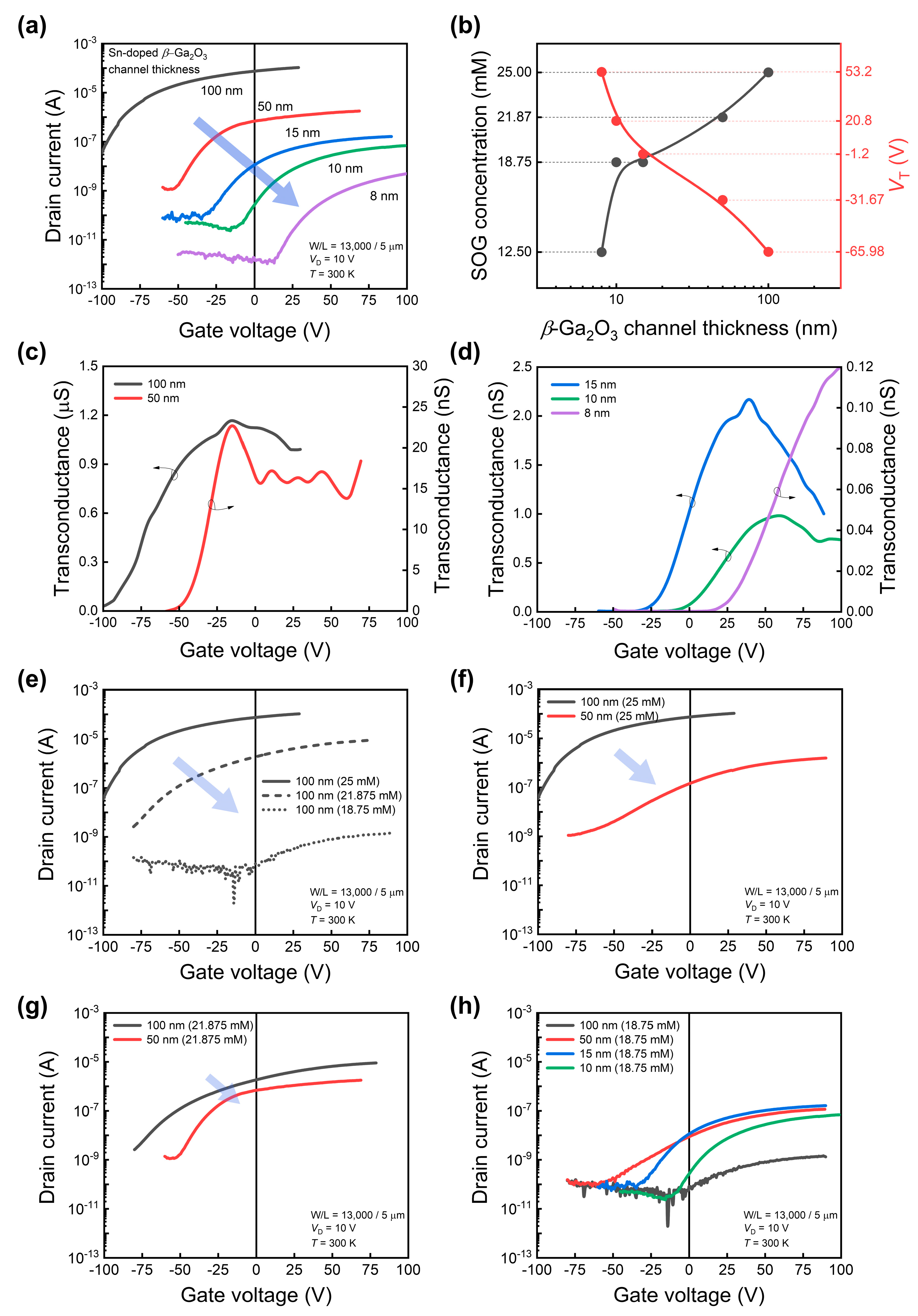
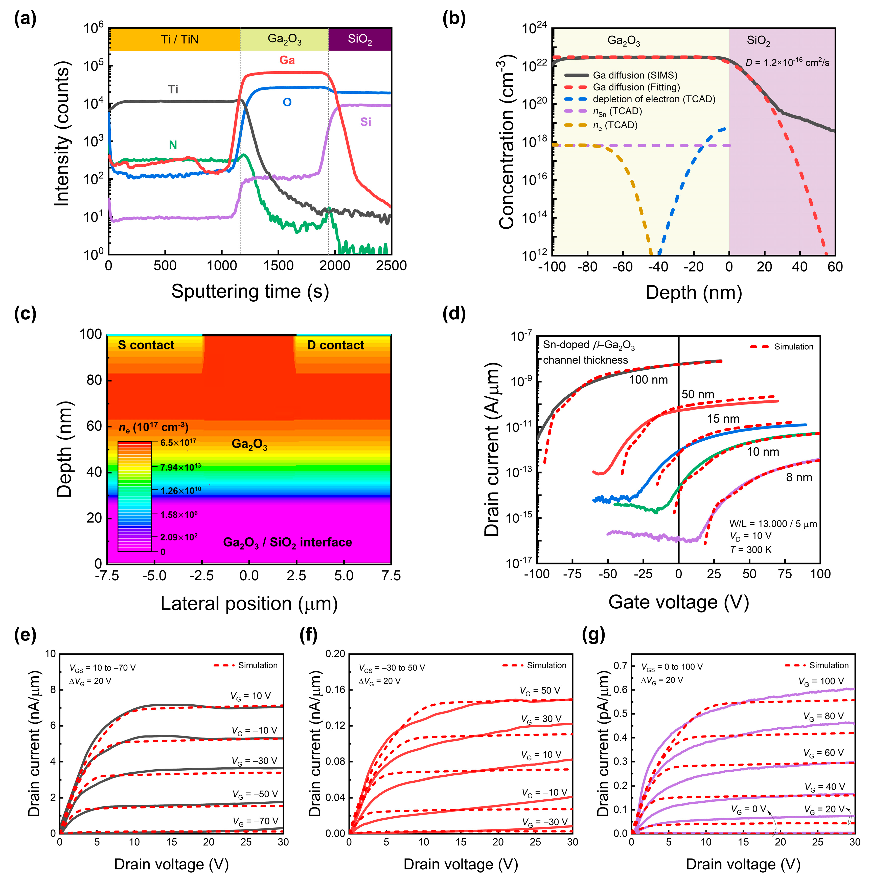
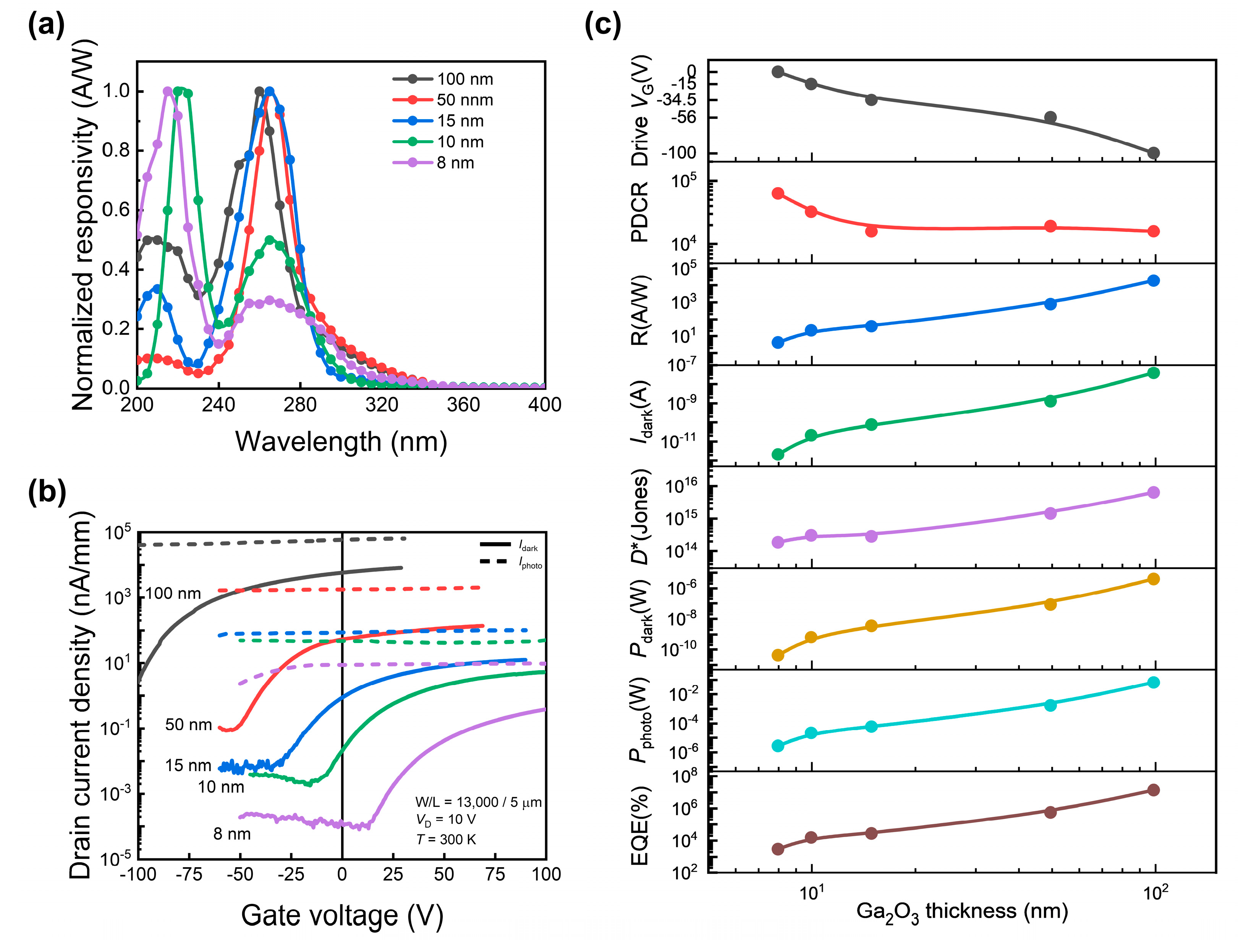
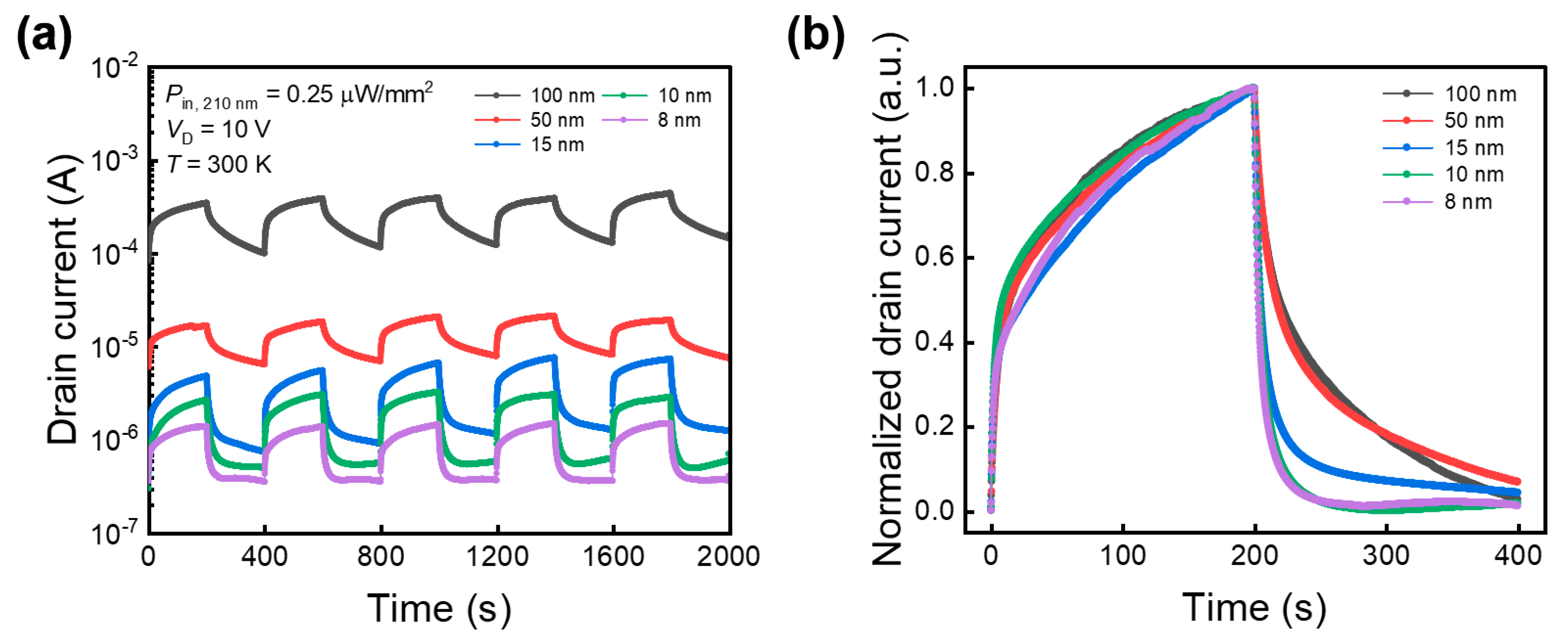
3. Results and Discussion

The schematic in Figure 1a shows that the Sn-doped polycrystalline β-Ga2O3 DUV phototransistor was fabricated in a back-gated stack structure. The source and drain electrodes were fabricated using Ti/TiN, the gate insulator was SiO2, and the gate was a p++-Si substrate. It has a typical phototransistor structure in which the photocurrent is output through the drain terminal when light is irradiated onto the top of the device. The upper left corner of Figure 1a shows an optical micrograph of the fabricated device. To maximize the width of the transistor within the same area, a pattern was designed in which the source and drain electrodes were interlocked in the form of pods. The length and width of the fingers are 500 and 5 μm, respectively, and the number of fingers on the electrode pad on one side is 13. The gap between the two crossed fingers to which the field is applied is designed to be 5 μm. The light-receiving area of the device, which is defined by the rectangular area indicated by the dotted line, was 0.125 mm2. Transmission electron microscopy (TEM) analysis was used to investigate the structural stability and crystalline properties of the fabricated device. Figure 1b shows the cross-sectional TEM images and fast Fourier transform (FFT) patterns of devices with Ga2O3 channel thicknesses of 100 and 8 nm, respectively. The FFT pattern of a square section randomly selected from the Ga2O3 region of the cross-sectional image was obtained, and the lattice spacing was extracted. The obtained lattice spacing values were selected and presented in Table 1, matching the monoclinic Ga2O3 JCPDS (reference code: 76-0573) within an error range of ±2%. Consistently, various planes were observed at thicknesses of 100 and 8 nm. Consequently, Ga2O3 exhibits the β-phase in the device and exists in a polycrystalline form.
Figure 1c shows the X-ray diffraction (XRD) analysis results for Ga2O3 subjected to various crystallization heat-treatment temperatures and Sn doping. Ga2O3 thin films deposited via sputtering have the advantage of large-area deposition; however, crystallization annealing is required to obtain device stability because they become amorphous immediately after deposition. β-Ga2O3 is a thermally and chemically stable phase, requiring high-temperature annealing to form the β-phase. Annealing was performed for 1 h in an Ar atmosphere with temperatures ranging from 800 to 1100 °C (black, red, blue, and green curves). As shown in the XRD results, increasing the annealing temperature improved the crystallinity and increased the peak intensity. Considering process efficiency (under 1000 °C), 900 °C was selected as the optimal crystallization annealing temperature. After crystallization annealing, a SOG process was used for Sn doping. Figure 1c presents the results for an SOG doping concentration of 0.025 M. Detailed information is provided in the experimental section. The purple curve represents the case where SOG doping was applied after crystallization heat treatment at 900 °C. The XRD peak results show that the β-phase was normally formed even after doping. Figure 1d,e show the transmittance and Tauc plot, respectively, for β-Ga2O3 thin films with thicknesses of 100, 50, and 8 nm, with and without doping. The results are consistent with the typical optical properties of β-Ga2O3, which exhibits near-transparency in the visible light region and absorbs light in the ultraviolet region.
The optical bandgap of each sample was estimated by extrapolating from the take-off area of the Tauc plot. For the intrinsic films with thicknesses of 100, 50, and 8 nm, the estimated band gaps were 4.82, 5.25, and 5.45 eV, respectively. The bandgaps of the Sn-doped films were 4.79, 5.13, and 5.31 eV, respectively. A consistent bandgap reduction was observed in the doped samples. This was due to the creation of a doping level at the bottom of the conduction band by doping with Sn, which acted as a donor. Additionally, as the thickness of Ga2O3 decreased, the band gap increased, which can be interpreted as a quantum confinement effect as the thin film thickness decreased. Consequently, it was confirmed that the phototransistor composed of Sn-doped β-Ga2O3 channels is suitable for absorption in the DUV region.
Next, we investigated the electrical characteristics of the fabricated Sn-doped β-Ga2O3 phototransistor under dark conditions. Figure 2a shows the transfer curves in the dark for Sn-doped β-Ga2O3 phototransistors fabricated with β-Ga2O3 channel thicknesses of 100, 50, 15, 10, and 8 nm, respectively. As the β-Ga2O3 channel thickness decreases, the transfer curve shifts downward, and the VT of the phototransistor changes from a negative to a positive value. Here, VT is extracted as the x-axis (gate voltage) intercept value of the extrapolated line drawn at the maximum drain current slope point on the transfer curves on a linear scale. In other words, the device transitions from d-mode to e-mode operation. This can be interpreted as an effect of the channel thickness, assuming that the doping concentration range of the devices at each thickness is similar. When different materials are stacked in a device, the energy-band structure is aligned based on the Fermi level at equilibrium. Owing to the difference in work functions between the bottom p++-Si gate and β-Ga2O3, depletion occurs at the interface where the β-Ga2O3 channel, which has a relatively small carrier concentration, contacts SiO2. This depletion thickness remains constant near the interface even if the channel thickness changes, assuming that the doping concentrations are similar. If the channel is sufficiently thick (e.g., 100 nm), neutral and n-type regions appear at a distance from the interface boundary. However, as the channel thickness decreases, the depletion region dominates the entire channel, gradually causing VT to shift in the positive direction. Consequently, the 8 nm-thick channel remains fully depleted at equilibrium, achieving e-mode operation with a positive VT.
The SOG doping process involves spin-coating an SOG solution containing a Sn source on the surface, followed by drive-in annealing. Devices with different β-Ga2O3 thicknesses require optimization of the SOG solution concentration suitable for each thickness condition. The results of the optimization of the molar concentration of the SOG doping solution for various thicknesses are presented in Table 2. The higher the molar concentration, the higher the amount of the Sn source. The optimal concentration of the SOG solution for a 100 nm thickness was 25 mM, while the optimized concentrations for 50, 15, 10, and 8 nm were 21.875, 18.75, 18.75, and 12.5 mM, respectively. By converting these molar values into weights, the values were found to be 0.875, 0.75, 0.75, and 0.5 based on a thickness of 100 nm. Figure 2b shows the optimal SOG concentration and VT change according to the β-Ga2O3 channel thickness. It was confirmed that the optimal SOG concentration had a non-linear correlation with the β-Ga2O3 channel thickness. Transfer curves were compared for a more detailed analysis by maintaining either the β-Ga2O3 thickness or the SOG doping concentration and varying the other parameters. Figure 2c,d show the transconductance for each thickness extracted from the transfer curves in Figure 2a.
Figure 2e represents the case with the β-Ga2O3 thickness constant at 100 nm and a varying SOG doping concentration. As the doping concentration decreases, the curves shift downward to the right, and VT becomes positive. This is likely due to an increase in the depletion area of the channel as the doping concentration decreases. In addition, the slope of the transfer curves corresponding to the current take-off gradually decreases. As the carrier concentration in the channel decreased, the channel and contact resistances increased. Figure 2f–h show the results for a constant SOG doping concentration and varying β-Ga2O3 thickness. In Figure 2f,g, the transfer curves shift downward to the right as the thickness decreases. Figure 2h illustrates the cases for an SOG doping concentration of 18.75 mM and a β-Ga2O3 thickness of 100, 50, 15, 10, and 8 nm. The 100 nm device has the lowest current owing to insufficient doping relative to its thickness. The 50 nm device also shows a high-resistance channel with a relatively flat slope. The 15 and 10 nm curves are relatively steep, indicating an appropriate doping concentration level. In this case, the transfer curves tend to shift downward to the right as the thickness decreases from 15 to 10 nm. It was confirmed that VT varied depending on the channel thickness and doping concentration. Additionally, because the channel resistance changes with the doping concentration, to obtain a positive VT without a loss of channel current, an additional process, such as applying local doping in the source–drain region, must be implemented to achieve e-mode operation.
Next, the results of analyzing the transfer curves of Sn-doped polycrystalline β-Ga2O3 phototransistors in the dark, using TCAD device simulation, are presented. To model the device’s VT change depending on the Ga2O3 channel thickness, the measured value could not be matched simply by channel depletion. Therefore, we considered the impact of Ga diffusion during the device fabrication process. Figure 3a shows the secondary ion mass spectrometry (SIMS) depth profile in the layered structure after a 900 °C crystallization annealing process. From the interface, Ga diffuses into SiO2. The lack of Ga in Ga2O3 can be interpreted as reducing the electron concentration. This effect may reduce the electron concentration in the Ga2O3 channel region adjacent to the SiO2 interface and affect the threshold voltage. For bulk materials with sufficiently thick channels, the influence of these interfaces is minimal. However, thinner materials have a larger surface-to-volume ratio and are significantly affected by surface and interface phenomena. Based on this analysis, we prepared the doping profile (TCAD profile in Figure 3b) and performed the TCAD simulation to understand the device operation. The concentration of Ga diffused into the SiO2 decreases steadily from the interface and exhibits a sudden change in gradient at an intermediate point. The region with a steep gradient before the inflection point is generally interpreted as direct volume diffusion, while the region with a shallow gradient after the inflection point is interpreted as grain boundary diffusion [42,43]. Since the direct volume diffusion region shows a significant concentration level, we focused on fitting the diffusion equation to this region. The complementary error function (ERFC) diffusion equation was applied to reflect the diffusion of Ga in the simulations. Equation (1) represents the concentration profile (N(x, t), atoms/cm3) used in Ga diffusion modeling.
N x ,   t = N 0 e r f c [ x 2 D t ]
where x is depth position (nm), D is the temperature-dependent diffusivity (cm2/s), and t is the diffusion time (s). Figure 3b shows the result of fitting the Ga diffusion profile obtained from SIMS to the ERFC diffusion equation. From the previous TEM analysis, we determined the thickness of each stacked material, allowing us to approximate the sputtering time in nanometers. However, since the sputtering rates differ for each material, reference tests for each material with known thicknesses are necessary to obtain an accurate depth. The results of fitting the diffusion equation are shown as red dashed lines. The diffusivity corresponding to this curve was found to be 1.2 × 10⁻¹⁶ cm2/s. The dashed lines illustrate the dopant and electron concentrations due to Ga diffusion, as reflected in the TCAD simulation.
To account for the effects of Ga diffusion into SiO2 and the depletion of electrons in the Ga2O3 channel, we assumed a p-type counter-doping scenario from the Ga2O3/SiO2 interface into the Ga2O3 region. This results in electron depletion of the Ga2O3 channel in the thin sections adjacent to the interface. As Ga diffuses into SiO2, Ga deficiency occurs in the Ga2O3 channel, which is indicated by the blue dashed depletion of the electron curve. nSn represents the electron concentration in the channel caused by SOG doping. Previous research has confirmed that the Sn concentration in the channel remains constant during SOG doping; accordingly, nSn is assumed to have a continuous value in the channel [44]. The concentration at the starting point where electron depletion occurs was optimized to a value between the maximum concentration of Ga and nSn. The final electron concentration (ne) profile, reflecting the combined effects of SOG doping and Ga diffusion, is shown as a dotted ocher line. These analyses were applied to TCAD simulations, and the materials and physical parameters used are presented in Table 3.
The Shockley–Read–Hall (SRH) model, which is fundamental for metal–oxide–semiconductor FET simulation, was used, and the energy band gap values were derived from previous transmittance measurements. Figure 3c shows the simulated color contours of the ne of a 100 nm-thick Sn-doped β-Ga2O3 channel. The electron concentration decreases exponentially as a function of distance from the channel surface, and the Ga2O3/SiO2 interfacial channel becomes completely depleted at approximately 20 nm. Figure 3d shows the results of matching the transfer curves for each thickness of β-Ga2O3 in a dark room through the TCAD device simulation, which matches well with the measured results. The donor concentration, which most directly affects VT, was optimized to 6.5 × 1017 cm−3 for the 100 nm device and appropriately scaled for the 50, 15, 10, and 8 nm devices by adjusting the SOG doping concentration weight ratio. The theoretical limit of electron mobility in single-crystal β-Ga2O3 is 300 cm2/Vs [49]. However, in this study, the Ga2O3 channel formed is a polycrystalline thin film. Thus, lattice scattering is accompanied by scattering due to grain boundaries and defects. Additionally, since Ga2O3 has extremely low thermal conductivity (10~30 W/m K) [45], mobility degradation can also occur due to internal heat accumulation [50,51]. Considering these causes of mobility degradation, the value was optimized to be lower than the ideal value. The fabricated Sn-doped β-Ga2O3 phototransistors exhibited somewhat leaky SiO2 due to the high-temperature crystallization annealing process at 900 °C. Consequently, the off-current of the device is similar to the gate leakage current. Although this leakage current was not reflected in this simulation, it can be optimized by applying a gate leakage current model. Figure 3e–g show the measured output characteristic curves and simulation matching results for devices with channel thicknesses of 100, 50, and 8 nm, respectively. Typical n-type conduction characteristics are confirmed, with a channel formed according to the positive gate voltage, and linear and saturation regions are confirmed.
We measured and characterized the optical performance of the Sn-doped β-Ga2O3 phototransistors. Figure 4a shows their normalized spectral responsivity measurements for different channel thicknesses. The 100, 50, and 15 nm channels showed peak photoresponsivity at 260, 265, and 265 nm. However, for the 15, 10, and 8 nm channels, the peak response wavelengths were 220 and 215 nm, respectively. This shift can be attributed to the quantum confinement effect, which increases the bandgap as the film becomes thinner. Additionally, the reduced thickness results in an insufficient absorption depth at longer wavelengths, leading to improved wavelength-selective responsivity. High sensitivity is maintained at shorter wavelengths and sensitivity is suppressed at longer wavelengths. This is advantageous for solar-blind UV detectors. Figure 4b presents the Idark and Iphoto transfer curves of Sn-doped β-Ga2O3 phototransistors for each channel thickness, measured under 210 nm monochromatic light, to compare DUV response characteristics. Photocurrent measurements were performed after more than 500 s of light irradiation to ensure saturation. The results demonstrate excellent light-response characteristics in the DUV region for all thicknesses. Figure 4c compares the photodetector performance parameters for each Ga2O3 thickness, derived from the Idark and Iphoto results shown in Figure 4b. The drive VG was selected as the smallest VG below the threshold voltage. Pdark and Pphoto represent the device power consumption under dark and illuminated conditions and were calculated as P = I D · V D + I G ·   V G 2 + V G V D 2 V G + V G V D , where I D and V D are drain current and voltage, and I G and V G are gate current and voltage, respectively [52,53]. As the Ga2O3 channel thickness decreased, the driving gate voltage approached zero, and the dark current decreased. For devices with a Ga2O3 thickness of 8 nm, Idark had the smallest value of 1.84 pA. This performance improvement was confirmed by the increased photo-to-dark current ratio (PDCR) caused by the reduced dark current. Conversely, with thicker channels, parameters such as responsivity (R), detectivity (D*), and external quantum efficiency (EQE), which are primarily related to the absolute value of the photocurrent, exhibited superior performance. Table 4 presents the detailed values of performance parameters of Sn-doped β-Ga2O3 phototransistors for each thickness tested in light and dark environments. Mobility was calculated using the μ = L W · 1 C o x · I D V G · 1 V D formula under dark conditions. Here, the relative permittivity of the SiO2 was calculated to be 3.9. The on–off ratio was calculated as the ratio of the maximum drain current to the minimum drain current in the transfer curves under dark conditions. For the 100 nm device, no clear device turn-off was observed within the measurement range, so the on–off ratio was not defined. In conclusion, the thickness of the Ga2O3 light-receiving channel is directly related to the photodetector performance parameters. These findings provide valuable insights and guidance for selecting the optimal thickness for the intended use of DUV phototransistors.
Figure 5a shows the time-dependent on–off response characteristics of the Sn-doped β-Ga2O3 phototransistors with varying thicknesses, measured under a 210 nm monochromatic light source. Owing to the polycrystalline structure, complete saturation takes hundreds of seconds because of scattering events and defects. However, the devices exhibited stable operational characteristics even after repeated cycling. Figure 5b normalizes one cycle to compare the light response speeds for each thickness. Although there was no significant difference in the rate of increase for different thicknesses, the decay rate increased as the thickness decreased. In bulk materials, charge carriers are scattered from various sources, including lattice vibrations (phonons), impurities, and defects [54]. However, when the light-absorption channel becomes sufficiently thin to constrain the dimensions, the carriers are confined to a single plane, reducing the number of scattering events. This reduced dimensionality suppresses electron–phonon interactions, leading to higher decay rates [55,56]. Therefore, decreasing the thickness of the Ga2O3 channel is advantageous in terms of light response speed. An improvement in response speed was confirmed as the thickness decreased, but from the perspective of commercialization of the device, a faster response speed is required. Accordingly, follow-up research is needed to improve the crystallinity of the thin films and suppress defects that affect photocurrent delay. From another perspective, the saturation and recovery delay of the photocurrent have potential applications in artificial neural networks where linearity and symmetry of the signal are significant, such as image generation and neural networks [57,58]. Table 5 shows the performance parameters and drive VG of the Sn-doped β-Ga2O3 phototransistors with 8 nm and 100 nm thicknesses, compared with other gallium oxide-based devices. The proposed Ga2O3 device has a usable performance level compared to the conventional results. When the channel thickness of the proposed device is reduced to 8 nm, the drive gate voltage can be set to zero due to the transition from d-mode to e-mode operation. As confirmed from the previously published results, the Ga2O3 channel thickness correlates with the drive VG. These results are significant in that the operation mode switching characteristics of Ga2O3 transistors, engineered from the perspective of optical devices, have practical implications in the field of semiconductor devices and optical engineering.

4. Conclusions

A Sn-doped polycrystalline β-Ga2O3-based phototransistor was fabricated through a sputtering process. The device was optimized from the d-mode to the e-mode through VT modulation achieved by Sn doping and channel thickness tuning. Additionally, the diffusion of Ga generated during the process was considered to affect the VT shift. Through TCAD device simulation, the transfer curves for each thickness in the dark were successfully matched, and the operation mode mechanism was analyzed. The proposed β-Ga2O3-based phototransistor was proven suitable for DUV detection through optical responsivity measurements. Moreover, as the Ga2O3 channel thickness decreased, the power consumption and response speed improved. However, the R, D*, and EQE performance, which are related to the absolute value of the photocurrent, improved with thickness. This study provides valuable insights and guidance for selecting the optimal thickness for the intended applications of DUV phototransistors. With the increasing potential of Ga2O3 in the power semiconductor field, the importance of achieving e-mode operation has also become a focal point. However, the quantitative and detailed mechanisms underlying e-mode and d-mode operation in the Ga2O3 field remain unresolved challenges. The VT control and optimization proposed in this study, along with the corresponding simulation analysis, will contribute to the technological maturation of the Ga2O3 field. Recently, there have been efforts to utilize machine learning algorithms to determine the optimal conditions for the devices. However, foundational datasets, like those proposed in this study, are essential for effective optimization using machine learning algorithms [69,70]. We anticipate that this research will serve as valuable data when machine learning is applied to various Ga2O3 applications in the future. Furthermore, as machine learning results accumulate, the key parameters used in device simulations are expected to become sufficiently reliable.

Author Contributions

Conceptualization, Y.Y. and M.S.; methodology, Y.Y.; validation, Y.K. and Y.Y.; formal analysis, Y.K.; investigation, Y.Y.; resources, M.S.; data curation, Y.K.; writing—original draft preparation, Y.Y.; writing—review and editing, M.S.; visualization, M.S.; supervision, M.S.; project administration, M.S.; funding acquisition, M.S. All authors have read and agreed to the published version of the manuscript.

Funding

This research was supported by a Korea Research Institute for Defense Technology Planning and Advancement (KRIT) grant funded by the Defense Acquisition Program Administration (DAPA) [grant number KRIT-CT-22-046], a National Research Foundation of Korea (NRF) grant funded by the Korean government (MSIT) (No. RS-2024-00352660)], and the K-Sensor Development Program (Grant No. RS-2022-00154729) funded by the Ministry of Trade, Industry, and Energy (MOTIE, Republic of Korea).

Institutional Review Board Statement

Not applicable.

Informed Consent Statement

Not applicable.

Data Availability Statement

The data presented in this study are available on request from the corresponding author.

Conflicts of Interest

The authors declare no conflicts of interest. The funders had no role in the design of the study; in the collection, analyses, or interpretation of data; in the writing of the manuscript; or in the decision to publish the results.

References

  1. Higashiwaki, M.; Jessen, G.H. Guest editorial: The dawn of gallium oxide microelectronics. Appl. Phys. Lett. 2018, 112, 060401. [Google Scholar] [CrossRef]
  2. Yamaguchi, K. First principles study on electronic structure of β-Ga2O3. Solid State Commun. 2004, 131, 739–744. [Google Scholar] [CrossRef]
  3. Dong, L.; Jia, R.; Xin, B.; Peng, B.; Zhang, Y. Effects of oxygen vacancies on the structural and optical properties of β-Ga2O3. Sci. Rep. 2017, 7, 40160. [Google Scholar] [CrossRef]
  4. Víllora, E.G.; Yamaga, M.; Inoue, T.; Yabasi, S.; Masui, Y.; Sugawara, T.; Fukuda, T. Optical spectroscopy study on β-Ga2O3. Jpn. J. Appl. Phys. 2002, 41, L622–L625. [Google Scholar] [CrossRef]
  5. Razeghi, M. Short-wavelength solar-blind detectors-status, prospects, and markets. Proc. IEEE 2002, 90, 1006–1014. [Google Scholar] [CrossRef]
  6. Sang, L.; Liao, M.; Sumiya, M. A Comprehensive review of semiconductor ultraviolet photodetectors: From thin film to one-dimensional nanostructures. Sensors 2013, 13, 10482–10518. [Google Scholar] [CrossRef] [PubMed]
  7. Guo, D.; Wu, Z.; Li, P.; An, Y.; Liu, H.; Guo, X.; Yan, H.; Wang, G.; Sun, C.; Li, L.; et al. Fabrication of β-Ga2O3 thin films and solar-blind photodetectors by laser MBE technology. Opt. Mater. Express 2014, 4, 1067. [Google Scholar] [CrossRef]
  8. Malik, M.; Iqbal, M.A.; Choi, J.R.; Pham, P.V. 2D Materials for efficient photodetection: Overview, mechanisms, performance and UV-IR range applications. Front. Chem. 2022, 10, 905404. [Google Scholar] [CrossRef]
  9. Yadav, P.V.K.; Ajitha, B.; Kumar Reddy, Y.A.; Sreedhar, A. Recent advances in development of nanostructured photodetectors from ultraviolet to infrared region: A Review. Chemosphere 2021, 279, 130473. [Google Scholar] [CrossRef]
  10. Arora, K.; Goel, N.; Kumar, M.; Kumar, M. Ultrahigh performance of self-powered β-Ga2O3 thin film solar-blind photodetector grown on cost-effective Si substrate using high-temperature seed layer. ACS Photonics 2018, 5, 2391–2401. [Google Scholar] [CrossRef]
  11. Bae, J.; Jeon, D.-W.; Park, J.-H.; Kim, J. High responsivity solar-blind metal-semiconductor-metal photodetector based on α-Ga2O3. J. Vac. Sci. Technol. A 2021, 39, 033410. [Google Scholar] [CrossRef]
  12. Kim, S.; Yoon, Y.; Seo, D.; Park, J.-H.; Jeon, D.-W.; Hwang, W.S.; Shin, M. Alpha-phase gallium oxide-based UVC photodetector with high sensitivity and visible blindness. APL Mater. 2023, 11, 061107. [Google Scholar] [CrossRef]
  13. Mi, W.; Tang, J.; Chen, X.; Li, X.; Li, B.; Luo, L.; Zhou, L.; Chen, R.; Wang, D.; Zhao, J. Preparation and UV detection performance of Ti-doped Ga2O3/intrinsic-Ga2O3/p-Si PIN photodiodes. J. Mater. Sci. Mater. Electron. 2023, 34, 774. [Google Scholar] [CrossRef]
  14. Vasquez, J.M.T.; Ashai, A.; Lu, Y.; Khandelwal, V.; Rajbhar, M.; Kumar, M.; Li, X.; Sarkar, B. A self-powered and broadband UV PIN photodiode employing a NiOx layer and a β-Ga2O3 heterojunction. J. Phys. D Appl. Phys. 2023, 56, 065104. [Google Scholar] [CrossRef]
  15. Kim, H.; Kim, K.; Hong, J. High performance deep ultraviolet P-i-n self-powered photodetector based on p-NiO/i-β-Ga2O3/n-β-Ga2O3 with controlled a fermi level and used an intrinsic β-Ga2O3 Layer. IEEE Sens. J. 2024, 24, 17613–17621. [Google Scholar] [CrossRef]
  16. Nandi, A.; Rana, K.S.; Bag, A. Design and analysis of P-GaN/N-Ga2O3 based junction barrier Schottky diodes. IEEE Trans. Electron. Devices 2021, 68, 6052–6058. [Google Scholar] [CrossRef]
  17. Liu, Z.; Tang, W. A Review of Ga2O3 deep-ultraviolet metal–semiconductor Schottky photodiodes. J. Phys. D Appl. Phys. 2023, 56, 093002. [Google Scholar] [CrossRef]
  18. Suzuki, R.; Nakagomi, S.; Kokubun, Y.; Arai, N.; Ohira, S. Enhancement of responsivity in solar-blind β-Ga2O3 photodiodes with a Au Schottky contact fabricated on single crystal substrates by annealing. Appl. Phys. Lett. 2009, 94, 222102. [Google Scholar] [CrossRef]
  19. Watahiki, T.; Yuda, Y.; Furukawa, A.; Yamamuka, M.; Takiguchi, Y.; Miyajima, S. Heterojunction p-Cu2O/n-Ga2O3 diode with high breakdown voltage. Appl. Phys. Lett. 2017, 111, 222104. [Google Scholar] [CrossRef]
  20. Nakagomi, S.; Momo, T.; Takahashi, S.; Kokubun, Y. Deep ultraviolet photodiodes based on β-Ga2O3/SiC heterojunction. Appl. Phys. Lett. 2013, 103, 072105. [Google Scholar] [CrossRef]
  21. Chi, P.-F.; Lin, F.-W.; Lee, M.-L.; Sheu, J.-K. High-responsivity solar-blind photodetectors formed by Ga2 O3/p-GaN bipolar heterojunctions. ACS Photonics 2022, 9, 1002–1007. [Google Scholar] [CrossRef]
  22. Kim, S.; Oh, S.; Kim, J. Ultrahigh deep-UV sensitivity in graphene-gated β-Ga2O3 phototransistors. ACS Photonics 2019, 6, 1026–1032. [Google Scholar] [CrossRef]
  23. Liu, Z.; Zhang, M.; Yang, L.; Li, S.; Zhang, S.; Li, K.; Li, P.; Guo, Y.; Tang, W. Enhancement-mode normally-off β-Ga2O3:Si metal-semiconductor field-effect deep-ultraviolet phototransistor. Semicond. Sci. Technol. 2022, 37, 015001. [Google Scholar] [CrossRef]
  24. Yoon, Y.; Kim, Y.; Hwang, W.S.; Shin, M. Biological UV photoreceptors-inspired Sn-Doped polycrystalline β-Ga2O3 optoelectronic synaptic phototransistor for neuromorphic computing. Adv. Electron. Mater. 2023, 9, 2300098. [Google Scholar] [CrossRef]
  25. Yoon, Y.; Hwang, W.S.; Shin, M. Solar-blind ultrathin Sn-doped polycrystalline Ga2O3 UV phototransistor for normally off operation. Adv. Photonics Res. 2022, 3, 2100316. [Google Scholar] [CrossRef]
  26. Liang, H.; Han, Z.; Mei, Z. Recent progress of deep ultraviolet photodetectors using amorphous gallium oxide thin films. Phys. Status Solidi A 2021, 218, 2000339. [Google Scholar] [CrossRef]
  27. Xu, J.; Zheng, W.; Huang, F. Gallium oxide solar-blind ultraviolet photodetectors: A Review. J. Mater. Chem. C Mater. 2019, 7, 8753–8770. [Google Scholar] [CrossRef]
  28. Kaur, D.; Kumar, M. A strategic review on gallium oxide based deep-ultraviolet photodetectors: Recent progress and future prospects. Adv. Opt. Mater. 2021, 9, 2002160. [Google Scholar] [CrossRef]
  29. Wong, M.H.; Lin, C.-H.; Kuramata, A.; Yamakoshi, S.; Murakami, H.; Kumagai, Y.; Higashiwaki, M. Acceptor doping of β-Ga2O3 by Mg and N ion implantations. Appl. Phys. Lett. 2018, 113, 102103. [Google Scholar] [CrossRef]
  30. Kyrtsos, A.; Matsubara, M.; Bellotti, E. On the feasibility of p-Type Ga2O3. Appl. Phys. Lett. 2018, 112, 032108. [Google Scholar] [CrossRef]
  31. Neal, A.T.; Mou, S.; Rafique, S.; Zhao, H.; Ahmadi, E.; Speck, J.S.; Stevens, K.T.; Blevins, J.D.; Thomson, D.B.; Moser, N.; et al. Donors and deep acceptors in β-Ga2O3. Appl. Phys. Lett. 2018, 113, 062101. [Google Scholar] [CrossRef]
  32. Robertson, J.; Clark, S.J. Limits to doping in oxides. Phys. Rev. B 2011, 83, 075205. [Google Scholar] [CrossRef]
  33. Petti, L.; Münzenrieder, N.; Vogt, C.; Faber, H.; Büthe, L.; Cantarella, G.; Bottacchi, F.; Anthopoulos, T.D.; Tröster, G. Metal oxide semiconductor thin-film transistors for flexible electronics. Appl. Phys. Rev. 2016, 3, 021303. [Google Scholar] [CrossRef]
  34. Yu, X.; Marks, T.J.; Facchetti, A. Metal oxides for optoelectronic applications. Nat. Mater. 2016, 15, 383–396. [Google Scholar] [CrossRef] [PubMed]
  35. Walsh, A.; Butler, K.T. Prediction of electron energies in metal oxides. Acc. Chem. Res. 2014, 47, 364–372. [Google Scholar] [CrossRef]
  36. Kamimura, T.; Nakata, Y.; Wong, M.H.; Than, P.H.; Higashiwaki, M. Nitrogen-Doped Channel β-Ga2O3 MOSFET with Normally-Off Operation. In Proceedings of the 2019 Compound Semiconductor Week (CSW), Nara, Japan, 19–23 May 2019; p. 1. [Google Scholar]
  37. Chabak, K.D.; McCandless, J.P.; Moser, N.A.; Green, A.J.; Mahalingam, K.; Crespo, A.; Hendricks, N.; Howe, B.M.; Tetlak, S.E.; Leedy, K.; et al. Recessed-gate enhancement-mode β-Ga2O3 MOSFETs. IEEE Electron. Device Lett. 2018, 39, 67–70. [Google Scholar] [CrossRef]
  38. Kachhawa, P.; Chaturvedi, N. A simulation approach for depletion and enhancement mode in β-Ga2O3 MOSFET. IETE Tech. Rev. 2022, 39, 1410–1418. [Google Scholar] [CrossRef]
  39. Chen, X.; Li, F.; Hess, H.L. Trench gate β-Ga2O3 MOSFETs: A review. Eng. Res. Express 2023, 5, 012004. [Google Scholar] [CrossRef]
  40. Zhou, H.; Si, M.; Alghamdi, S.; Qiu, G.; Yang, L.; Peide, D.Y. High-Performance Depletion/Enhancement-mode β-Ga2O3 on Insulator (GOOI) Field-Effect Transistors with Record Drain Currents of 600/450 mA/mm. IEEE Electron. Device Lett. 2016, 38, 103–106. [Google Scholar] [CrossRef]
  41. Sharma, R.; Patnaik, A.; Sharma, P. Impact of doping concentration and recess depth to achieve enhancement mode operation in β-Ga2O3 MOSFET. Microelectron. J. 2023, 135, 105755. [Google Scholar] [CrossRef]
  42. Gurbán, S.; Sulyok, A.; Menyhárd, M.; Baradács, E.; Parditka, B.; Cserháti, C.; Erdélyi, Z. Interface induced diffusion. Sci. Rep. 2021, 11, 9308. [Google Scholar] [CrossRef] [PubMed]
  43. Laemmle, A.; Wuerz, R.; Schwarz, T.; Cojocaru-Mirédin, O.; Choi, P.P.; Powalla, M. Investigation of the diffusion behavior of sodium in Cu (In, Ga) Se2 layers. J. Appl. Phys. 2014, 115, 154501. [Google Scholar] [CrossRef]
  44. Yoon, Y.; Kim, S.; Lee, I.G.; Cho, B.J.; Hwang, W.S. Electrical and photocurrent properties of a polycrystalline Sn-doped β-Ga2O3 thin film. Mater. Sci. Semicond. Process. 2021, 121, 105430. [Google Scholar] [CrossRef]
  45. Higashiwaki, M.; Sasaki, K.; Murakami, H.; Kumagai, Y.; Koukitu, A.; Kuramata, A.; Yamakoshi, S. Recent progress in Ga2O3 power devices. Semicond. Sci. Technol. 2016, 31, 034001. [Google Scholar] [CrossRef]
  46. Kotecha, R.; Metzger, W.; Mather, B.; Narumanchi, S.; Zakutayev, A. Modeling and analysis of gallium oxide vertical transistors. ECS J. Solid State Sci. Technol. 2019, 8, Q3202. [Google Scholar] [CrossRef]
  47. Janowitz, C.; Scherer, V.; Mohamed, M.; Krapf, A.; Dwelk, H.; Manzke, R.; Van de Walle, C.G. Experimental electronic structure of In2O3 and Ga2O3. New J. Phys. 2011, 13, 085014. [Google Scholar] [CrossRef]
  48. Shockley, W.T.R.W.; Read, W.T., Jr. Statistics of the recombinations of holes and electrons. Phys. Rev. 1952, 87, 835. [Google Scholar] [CrossRef]
  49. Ma, N.; Tanen, N.; Verma, A.; Guo, Z.; Luo, T.; Xing, H.G.; Jena, D. Intrinsic electron mobility limits in β-Ga2O3. Appl. Phys. Lett. 2016, 109, 212101. [Google Scholar] [CrossRef]
  50. Park, J.; Hong, S.M. Simulation study of enhancement mode multi-gate vertical gallium oxide MOSFETs. ECS J. Solid State Sci. Technol. 2019, 8, Q3116. [Google Scholar] [CrossRef]
  51. Jang, C.H.; Atmaca, G.; Cha, H.Y. Normally-off β-Ga2O3 MOSFET with an epitaxial drift layer. Micromachines 2022, 13, 1185. [Google Scholar] [CrossRef]
  52. Xiao, X.; Liang, L.; Pei, Y.; Yu, J.; Duan, H.; Chang, T.-C.; Cao, H. Solution-processed amorphous Ga2O3:CdO TFT-type deep-UV photodetectors. Appl. Phys. Lett. 2020, 116, 192102. [Google Scholar] [CrossRef]
  53. Duan, H.; Javaid, K.; Liang, L.; Huang, L.; Yu, J.; Zhang, H.; Gao, J.; Zhuge, F.; Chang, T.-C.; Cao, H. Broadband optoelectronic synaptic thin-film transistors based on oxide semiconductors. Phys. Status Solidi Rapid Res. Lett. 2020, 14, 1900630. [Google Scholar] [CrossRef]
  54. Dongre, B.; Carrete, J.; Wen, S.; Ma, J.; Li, W.; Mingo, N.; Madsen, G.K. Combined treatment of phonon scattering by electrons and point defects explains the thermal conductivity reduction in highly-doped Si. J. Mater. Chem. 2020, 8, 1273–1278. [Google Scholar] [CrossRef]
  55. Turney, J.E.; McGaughey, A.J.; Amon, C.H. In-plane phonon transport in thin films. J. Appl. Phys. 2010, 107, 024317. [Google Scholar] [CrossRef]
  56. Cao, R.; Sun, K.; Liu, C.; Mao, Y.; Guo, W.; Ouyang, P.; Meng, Y.; Tian, R.; Xie, L.; Lü, X.; et al. Structurally Flexible 2D Spacer for Suppressing the Electron–Phonon Coupling Induced Non-Radiative Decay in Perovskite Solar Cells. Nanomicro Lett. 2024, 16, 178. [Google Scholar] [CrossRef]
  57. Ni, Y.; Zhang, S.; Sun, L.; Liu, L.; Wei, H.; Xu, Z.; Xu, W.; Xu, W. A low-dimensional hybrid pin heterojunction neuromorphic transistor with ultra-high UV sensitivity and immediate switchable plasticity. Appl. Mater. Today 2021, 25, 101223. [Google Scholar] [CrossRef]
  58. Gong, J.; Wei, H.; Ni, Y.; Zhang, S.; Du, Y.; Xu, W. Methylammonium halide-doped perovskite artificial synapse for light-assisted environmental perception and learning. Mater. Today Phys. 2021, 21, 100540. [Google Scholar] [CrossRef]
  59. Ahn, J.; Ma, J.; Lee, D.; Lin, Q.; Park, Y.; Lee, O.; Heo, J. Ultrahigh deep-ultraviolet responsivity of a β-Ga2O3/MgO heterostructure-based phototransistor. ACS Photonics 2021, 8, 557–566. [Google Scholar] [CrossRef]
  60. Qin, Y.; Long, S.; He, Q.; Dong, H.; Jian, G.; Zhang, Y.; Liu, M. Amorphous gallium oxide-based gate-tunable high-performance thin film phototransistor for solar-blind imaging. Adv. Electron. Mater. 2019, 5, 1900389. [Google Scholar] [CrossRef]
  61. Qin, Y.; Dong, H.; Long, S.; He, Q.; Jian, G.; Zhang, Y.; Liu, M. Enhancement-Mode β-Ga2O 3 Metal–Oxide–Semiconductor Field-Effect Solar-Blind Phototransistor with Ultrahigh Detectivity and Photo-to-Dark Current Ratio. IEEE Electron. Device Lett. 2019, 40, 742–745. [Google Scholar] [CrossRef]
  62. Xu, Y.; Cheng, Y.; Li, Z.; Feng, Q.; Zhang, Y.; Chen, D.; Hao, Y. High performance gate tunable solar blind ultraviolet phototransistors based on amorphous Ga2O3 films grown by mist chemical vapor deposition. Nano Sel. 2021, 2, 2112–2120. [Google Scholar] [CrossRef]
  63. Li, Z.; Feng, Z.; Xu, Y.; Feng, Q.; Zhu, W.; Chen, D.; Hao, Y. High performance β-Ga2O 3 solar-blind metal–oxide–semiconductor field-effect phototransistor with hafnium oxide gate dielectric process. IEEE Electron. Device Lett. 2021, 42, 545–548. [Google Scholar] [CrossRef]
  64. Yu, S.; Zhao, X.; Ding, M.; Tan, P.; Hou, X.; Zhang, Z.; Long, S. High-detectivity β-Ga2O3 microflake solar-blind phototransistor for weak light detection. IEEE Electron. Device Lett. 2021, 42, 383–386. [Google Scholar] [CrossRef]
  65. Kim, S.; Kim, J. Highly selective ozone-treated β-Ga2O3 solar-blind deep-UV photodetectors. Appl. Phys. Lett. 2020, 117, 261101. [Google Scholar] [CrossRef]
  66. Han, Z.; Liang, H.; Huo, W.; Zhu, X.; Du, X.; Mei, Z. Boosted UV photodetection performance in chemically etched amorphous Ga2O3 thin-film transistors. Adv. Opt. Mater. 2020, 8, 1901833. [Google Scholar] [CrossRef]
  67. Pintor-Monroy, M.I.; Reyes-Banda, M.G.; Avila-Avendano, C.; Quevedo-Lopez, M.A. Tuning electrical properties of amorphous Ga2O3 thin films for deep UV phototransistors. IEEE Sens. J. 2021, 21, 14807–14814. [Google Scholar] [CrossRef]
  68. Liu, Y.; Du, L.; Liang, G.; Mu, W.; Jia, Z.; Xu, M.; Song, A. Ga2O3 field-effect-transistor-based solar-blind photodetector with fast response and high photo-to-dark current ratio. IEEE Electron. Device Lett. 2018, 39, 1696–1699. [Google Scholar] [CrossRef]
  69. Roh, Y.; Heo, G.; Whang, S.E. A survey on data collection for machine learning: A big data-ai integration perspective. IEEE Trans. Knowl. Data Eng. 2019, 33, 1328–1347. [Google Scholar] [CrossRef]
  70. Uddin, S.; Lu, H. Dataset meta-level and statistical features affect machine learning performance. Sci. Rep. 2024, 14, 1670. [Google Scholar] [CrossRef]
Figure 1. (a) Schematic and optical micrograph and (b) cross-sectional transmission electron microscopy (TEM) images and their fast Fourier transform (FFT) patterns for the Sn-doped polycrystalline β-Ga2O3 deep ultraviolet (DUV) phototransistor. (c) X-ray diffraction (XRD) analysis results according to crystallization annealing temperature and Sn doping of Ga2O3 with a thickness of 100 nm. (d) Transmittance and (e) Tauc plot according to the presence or absence of β-Ga2O3 thin film doping with thicknesses of 100, 50, and 8 nm.
Sensors 24 05822 g001
Figure 2. (a) Transfer curves of Sn-doped β-Ga2O3 phototransistors fabricated with β-Ga2O3 channel thicknesses of 100, 50, 15, 10, and 8 nm. (b) Optimal spin-on-glass (SOG) doping concentration and corresponding VT change according to β-Ga2O3 channel thickness. Transconductance for each thickness (c) 100 and 50 nm, (d) 15, 10 and 8 nm. Each data point was calculated from the curves in (a). (e) Changes in transfer curves with a constant thickness of 100 nm and varying SOG doping concentrations. Changes in transfer curves for a constant SOG doping concentration and varying thickness at 100 nm and 50 nm (f) 25 mM, (g) 21.875 mM. (h) Transfer curves for a constant SOG doping concentration at 18.75 mM and varying thickness at 100, 50, 15, and 10 nm.
Sensors 24 05822 g002
Figure 3. (a) Secondary ion mass spectrometry (SIMS) analysis results of 100-nm thick β-Ga2O3 device subjected to crystallization annealing at 900 °C. (b) Ga diffusion profile fitted with a complementary error function (ERFC) and depletion of electrons caused by Ga diffusion, electron concentration by SOG doping (nSn), final electron concentration profile (ne) implemented through technology computer-aided design (TCAD) device simulation. (c) Color contours of the ne of 100 nm-thick Sn-doped β-Ga2O3 channel. Result of matching for each β-Ga2O3 thickness in a dark room through TCAD device simulation (d) transfer and (eg) output curves.
Sensors 24 05822 g003
Figure 4. (a) Normalized spectral responsivity, and (b) drain current density for dark current (Idark) and photocurrent (Iphoto) in transfer curves of fabricated Sn-doped β-Ga2O3 phototransistors according to channel thickness. In (b), a DUV monochromatic light source with a wavelength of 210 nm was used, with an optical power density (Pin) of 0.25 μW/mm2. (c) Photodetector performance comparison results of Sn-doped β-Ga2O3 phototransistors according to Ga2O3 thickness.
Sensors 24 05822 g004
Figure 5. (a) Time-dependent on–off response characteristics of the Sn-doped β-Ga2O3 phototransistors device by thickness measured by applying a 210 nm monochromatic light source. One cycle was performed over 400 s. (b) Normalized drain current comparison results for one cycle of optical switching investigation for each Ga2O3 thickness.
Sensors 24 05822 g005
Table 1. Comparison of bulk lattice parameters for different major planes in 8 nm- and 100 nm-thick Sn-doped polycrystalline β-Ga2O3.
PlanesLattice Spacing [Å]PlanesLattice Spacing [Å]
JCPDS8 nm Sn-Doped Polycrystalline β-Ga2O3JCPDS100 nm Sn-Doped Polycrystalline β-Ga2O3
(−401)2.9292.920(111)2.5492.549
(−111)2.6752.665(−311)2.3432.356
(002)2.8172.857(400)2.9712.998
(112)1.9781.962(401)2.4032.385
Table 2. Sn-doped polycrystalline β-Ga2O3 thickness and SOG solution concentration conditions.
β-Ga2O3 Thickness [nm]SOG Solution Concentration [mM]Doping Weight
100251
5021.8750.875
1518.750.75
1018.750.75
812.50.5
Table 3. Materials physical model parameters used in TCAD simulation of transfer curves of Sn-doped polycrystalline β-Ga2O3 phototransistors.
Material ParametersValuesUnitSource
Dielectric constant10unitless[45]
Electron affinity4eV[46]
Electron density of state (300 K)3.72 × 1018cm−3[47]
Shockley–Read–Hall Recombination (SRG) ModelValuesUnitSource
Specifies SRH lifetime for electrons1.2 × 10−8s[48]
Specifies SRH lifetime for holes1.2 × 10−8s[48]
Table 4. Comparison of performance parameters of each Sn-doped β-Ga2O3 phototransistor with various Ga2O3 thicknesses.
Parameterβ-Ga2O3 Thickness [nm]
1005015108
VT [V]−65.98−31.67−1.220.853.2
Mobility [cm2/V∙s]3.81 × 10−35.23 × 10−57.6 × 10−62.89 × 10−63.94 × 10⁻⁷
On–off ratio-1.66 × 1032.93 × 1033.7 × 1034.73 × 103
Drive VG [V]−100−56−34.5−150
PDCR1.57 × 1041.90 × 1041.55 × 1043.20 × 1046.19 × 104
R [A/W]1.73 × 1047.08 × 10234.219.43.7
Idark [A]3.39 × 10−81.15 × 10−96.75 × 10−111.86 × 10−111.84 × 10⁻¹²
D* [Jones]5.87 × 10151.31 × 10152.60 × 10142.80 × 10141.71 × 1014
Pdark [W]3.20 × 10−66.78 × 10−82.84 × 10−95.03 × 10−103.31 × 10⁻¹¹
Pphoto [W]5.01 × 10−21.29 × 10−34.42 × 10−51.61 × 10−52.05 × 10⁻⁶
EQE [%]1.02 × 1074.18 × 1052.02 × 1041.14 × 1042.19 × 103
Table 5. Comparison of performance parameters of Sn-doped β-Ga2O3 phototransistor with reported values from other gallium-oxide-based devices.
Channel Thickness [nm]Drive VG [V]R [A/W]Idark [A]PDCRD* [Jones]Ref.
803.71.84 × 10−126.19 × 1041.71 × 1014This work
100−1001.73 × 1043.39 × 10−81.57 × 1045.87 × 1015This work
280−82.6 × 1031.2 × 10−136 × 1089.7 × 1013[22]
270−202.4 × 1076.7 × 10−12-1.7 × 10¹⁵[59]
208−304.1 × 1032 × 10−11-2.57 × 10¹³[60]
200−53 × 1037 × 10−131.1 × 1061.3 × 1016[61]
267−102.3 × 10³≈1.5 × 10−96.67 × 1031.87 × 1014[62]
112−271.43 × 10⁷≈4.8 × 10−136.9 × 1071.1 × 1019[63]
217−101.17 × 1052.7 × 10−141.08 × 1071.19 × 1018[64]
381−39.51.93 × 1064.35 × 10−113.1 × 1081.9 × 1015[65]
400105.67 × 103≈1 × 10−125.7 × 1071.87 × 1015[66]
5901 × 1021 × 10−13≈3 × 1081 × 1015[67]
300.22.171.61 × 10−12≈1 × 1051.71 × 1012[52]
142−204.79 × 1059.91 × 10−121 × 1056.69 × 1014[68]
Disclaimer/Publisher’s Note: The statements, opinions and data contained in all publications are solely those of the individual author(s) and contributor(s) and not of MDPI and/or the editor(s). MDPI and/or the editor(s) disclaim responsibility for any injury to people or property resulting from any ideas, methods, instructions or products referred to in the content.

