

One-Dimensional ZnO Nanorod Array Grown on Ag Nanowire Mesh/ZnO Composite Seed Layer for H2 Gas Sensing and UV Detection Applications


Abstract
:1. Introduction
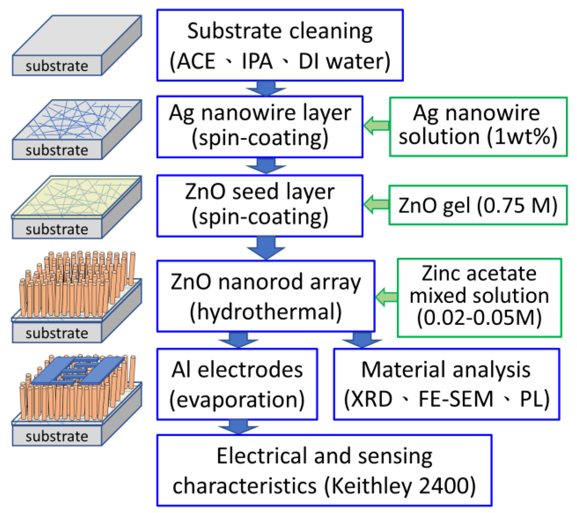
2. Materials and Methods
2.1. Formation of the Silver Nanowire Mesh
2.2. Formation of the Seed Layer
- Solution Preparation: A total of 6.5844 g of zinc acetate dihydrate was added to a beaker containing 38.2 mL of monoethanolamine (MEA, HOCH2CH2NH2) and 1.8 mL of ethylene glycol monomethyl ether (EGME, CH3OCH2CH2OH), resulting in a 0.75 M Zn2+ ion solution.
- Heating and Stirring: The mixture was heated and stirred at 60 °C for 2 h, then aged in an auto dry box at room temperature for 48 h to obtain a uniform and transparent ZnO gel solution.
- Spin Coating: The ZnO sol–gel solution was spin coated onto the substrates prepared in Section 2.1 at a rotation speed of 2000 rpm for 30 s.
- Baking and Cooling: The coated substrates were placed on a hot plate at 300 °C for 10 min and then allowed to cool for 10 min. The spin-coating, baking, and cooling steps were repeated once more to complete the ZnO seed layer formation.
2.3. Synthesis of the ZnO Nanorod Array
2.4. Characterization
2.4.1. Structural and Morphological Characterization
2.4.2. Optical Characterization
2.4.3. Device Fabrication and Electrical Measurements
3. Results and Discussion
3.1. ZnO Seed Layer Coated on Silver Nanowire Mesh
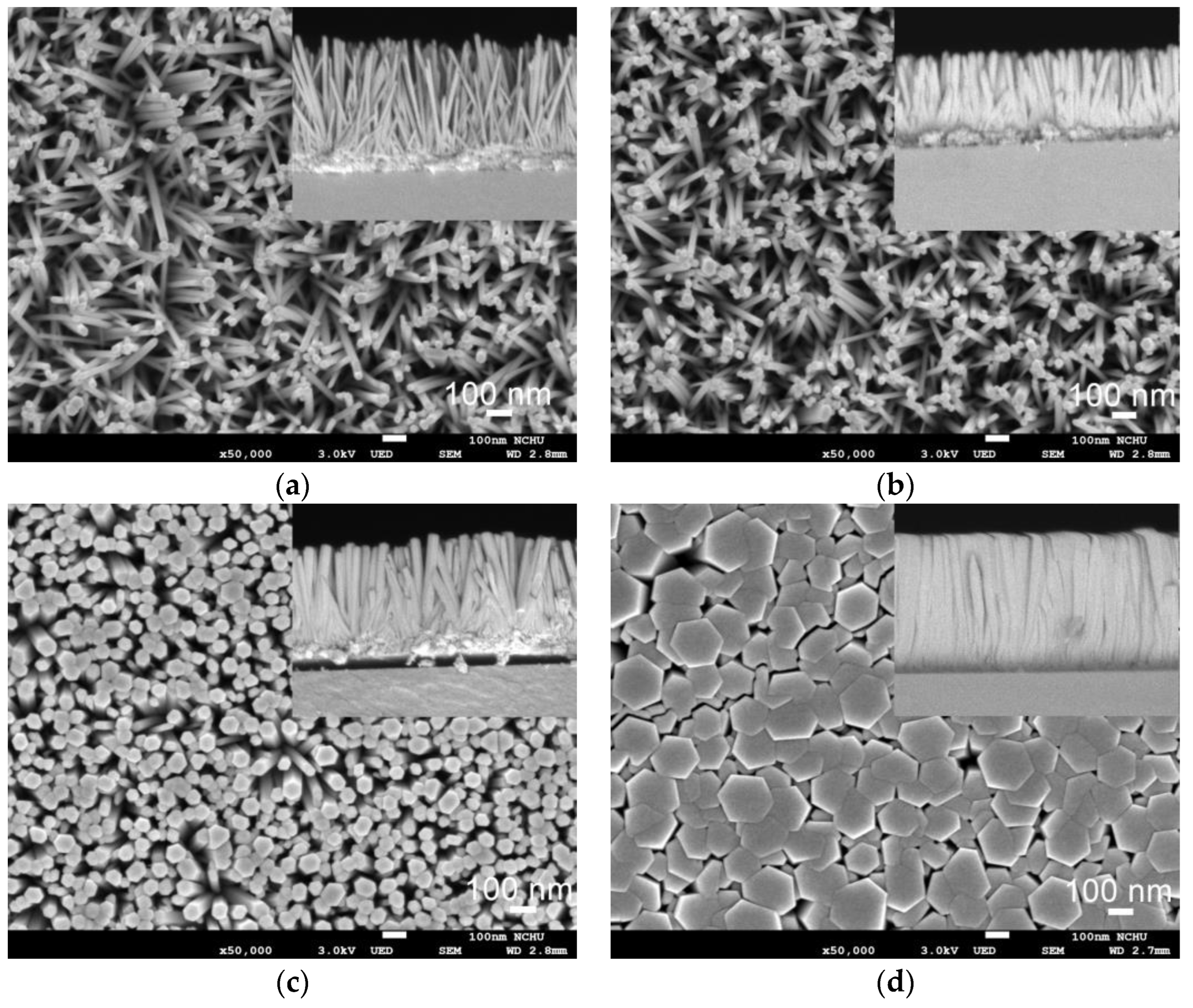
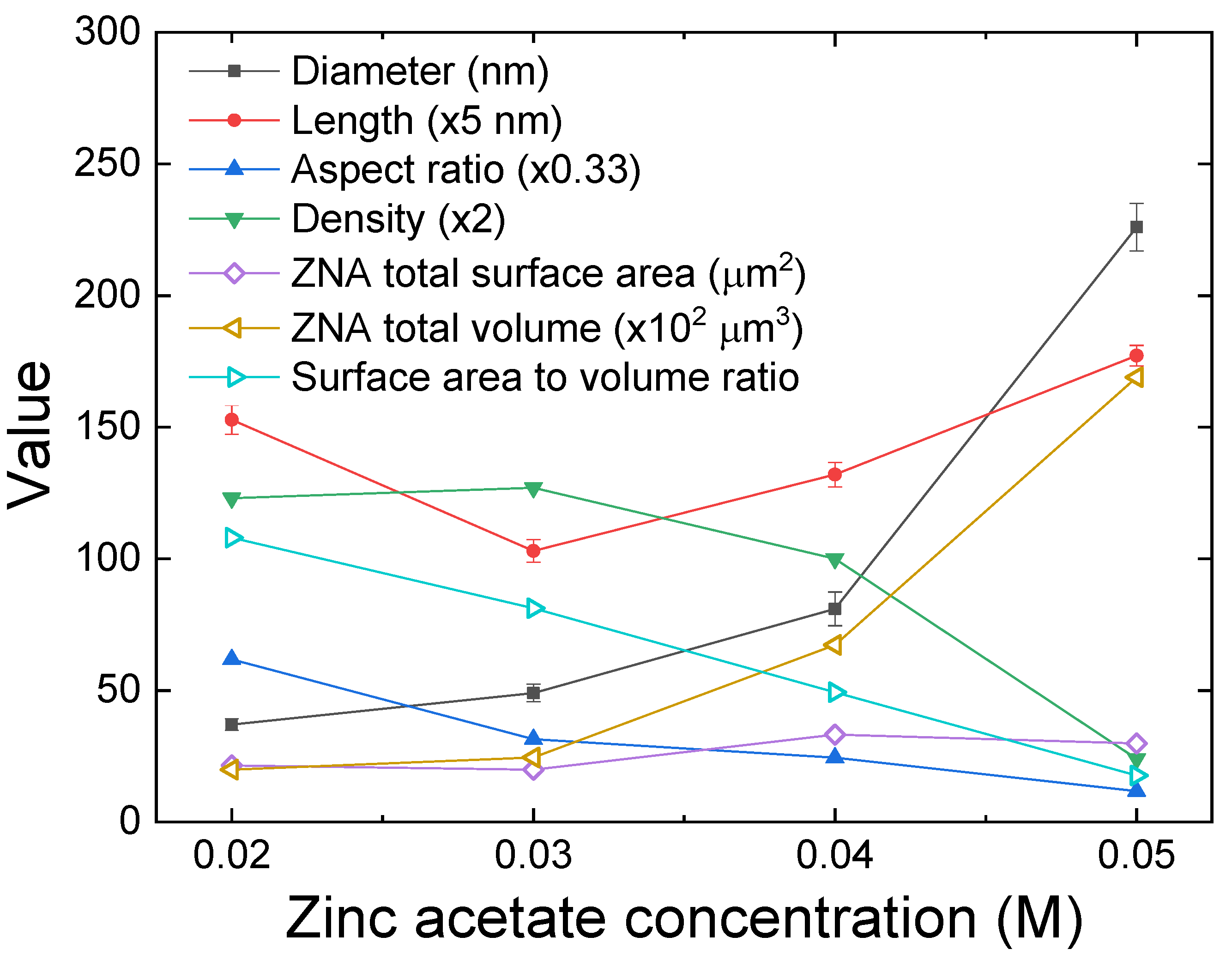
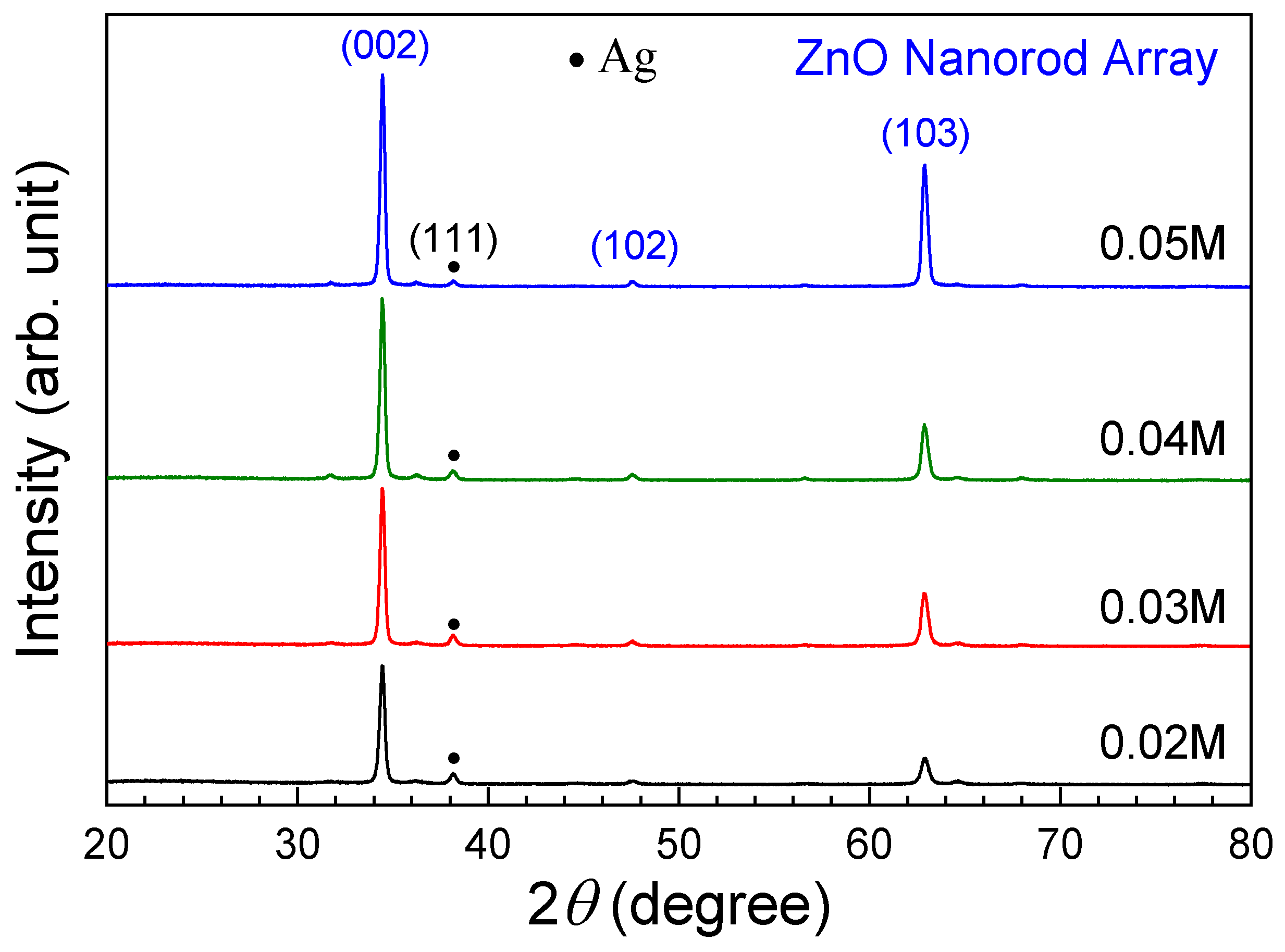
3.2. ZnO Nanorod Array
3.3. Gas Sensing Properties of ZNA-AgNMs
3.4. Photodetecting Properties of ZNA-AgNMs

| Device | Wavelength/ Voltage | Responsivity (A/W) | Detectivity (Jones) | Rise/Decay Time | Reference |
|---|---|---|---|---|---|
| Ag nanoparticle-ZNA | 395 nm/2 V | 0.04 | - | -/- | [15] |
| ZNA | 360 nm/5 V | 0.878 | - | 10.3 s/17.7 s | [48] |
| ZNA | 390 nm/−5 V | 2.19 | - | 0.49 s/1.14 s | [49] |
| PEI-ZNA | 365 nm/5 V | 43.7 | 1.85 × 10¹⁴ | 4.8 s/4.9 s | [44] |
| ZNA/CuO/p-GaN | 365 nm/0 V | 1.44 × 10⁻³ | 5.9 × 10¹⁰ | 0.12 s/0.22 s | [50] |
| ZNA/PEDOT:PSS | 364 nm/−2 V | 9.2 | 7.3 × 10¹² | 336 s/294 s | [51] |
| Ag-doped ZNA | 365 nm/5 V | 0.0173 | 2.18 × 10¹¹ | 7.4 s/26.9 s | [52] |
| Ga-doped ZNA | 360 nm/1 V | 0.046 | 3.92 × 10¹² | 89 s/106 s | [53] |
| Ga-doped ZnO NWs | 365 nm/0 V | 0.233 | 4.18 × 10¹² | 159 ms/150 ms | [54] |
| ZnO NWs on Ag NWs + Ag-paste | 365 nm/2 V | 54 | - | 0.2 s/0.1 s | [55] |
| ZnO/Ag NWs/ZnO | 365 nm/1 V | 0.1 | 6.8 × 10¹² | 2.15 s/2.44 s | [56] |
| ZNA on ZnO-AgNM layer | 374 nm/5 V | 114 | 6.37 × 10¹⁴ | -/- | This work |
4. Conclusions
Author Contributions
Funding
Institutional Review Board Statement
Informed Consent Statement
Data Availability Statement
Conflicts of Interest
References
- Peng, M.; Wen, Z.; Sun, X. Recent Progress of Flexible Photodetectors Based on Low-Dimensional II–VI Semiconductors and Their Application in Wearable Electronics. Adv. Funct. Mater. 2023, 33, 2211548. [Google Scholar] [CrossRef]
- Scarpa, G.; Idzko, A.L.; Yadav, A.; Martin, E.; Thalhammer, S. Toward Cheap Disposable Sensing Devices for Biological Assays. IEEE Trans. Nanotechnol. 2010, 9, 527–532. [Google Scholar] [CrossRef]
- Dey, M.; Chowdhury, S.; Kumar, S.; Kumar Singh, A. Quantum Confinement Effect on Defect Level of Hydrogen Doped Rutile VO2nanowires. J. Appl. Phys. 2022, 131, 235702. [Google Scholar] [CrossRef]
- Li, Z.; Hou, Y.; Ma, Y.; Zhai, F.; Joshi, M.K. Recent Advances in One-Dimensional Electrospun Semiconductor Nanostructures for UV Photodetector Applications: A Review. J. Alloys Compd. 2023, 948, 169718. [Google Scholar] [CrossRef]
- Weintraub, B.; Zhou, Z.; Li, Y.; Deng, Y. Solution Synthesis of One-Dimensional ZnO Nanomaterials and Their Applications. Nanoscale 2010, 2, 1573–1587. [Google Scholar] [CrossRef]
- Greeesan, R.; Jegan, J.; Kannaki, S.; Dineshkumar, S.; Kayalvizhi, A. Investigations on ZnO Reinforced Composite Materials for Electronic Applications—A Review. Mater. Today Proc. 2023, 74, 57–59. [Google Scholar] [CrossRef]
- Yoo, J.; Ahmed, T.; Tang, W.; Kim, Y.J.; Joon Hong, Y.; Lee, C.H.; Yi, G.C. Single Crystalline ZnO Radial Homojunction Light-Emitting Diodes Fabricated by Metalorganic Chemical Vapour Deposition. Nanotechnology 2017, 28, 394001. [Google Scholar] [CrossRef]
- Liu, Z.; Liu, S.; Wu, W.; Liu, C.R. The Mechanism of Controlled Integration of ZnO Nanowires Using Pulsed-Laser-Induced Chemical Deposition. Nanoscale 2019, 11, 2617–2623. [Google Scholar] [CrossRef] [PubMed]
- Zhu, J.; Feng, Y.; Dai, B.; Qi, Y. Morphology and Orientation Controlling of ZnO Nanofibers via Chemical Bath Deposition. Mater. Chem. Phys. 2023, 305, 128028. [Google Scholar] [CrossRef]
- Zhao, X.; Jheng, J.C.; Chou, N.N.; Wang, F.H.; Yang, C.F. Synthesis of ZnO Nanoflower Arrays on a Protrusion Sapphire Substrate and Application of Al-Decorated ZnO Nanoflower Matrix in Gas Sensors. Sensors 2023, 23, 5629. [Google Scholar] [CrossRef]
- Aidit, S.N.; Rezali, F.A.M.; Nor, N.H.M.; Yusoff, N.; Ma, L.Y.; Hatta, S.F.W.M.; Soin, N. Hydrothermal Synthesis of Zinc Oxide/PEDOT:PSS Composite for Flexible Temperature Sensor Application. Flex. Print. Electron. 2023, 8, 025008. [Google Scholar] [CrossRef]
- Jin, Y.; Wang, J.; Sun, B.; Blakesley, J.C.; Greenham, N.C. Solution-Processed Ultraviolet Photodetectors Based on Colloidal ZnO Nanoparticles. Nano Lett. 2008, 8, 1649–1653. [Google Scholar] [CrossRef] [PubMed]
- Shi, L. Flexible Transparent Silver Nanowires Conductive Films Fabricated with Spin-Coating Method. Micro Nano Lett. 2022, 18, e12151. [Google Scholar] [CrossRef]
- Mohammad, S.M.; Hassan, Z.; Talib, R.A.; Ahmed, N.M.; Al-Azawi, M.A.; Abd-Alghafour, N.M.; Chin, C.W.; Al-Hardan, N.H. Fabrication of a Highly Flexible Low-Cost H2 Gas Sensor Using ZnO Nanorods Grown on an Ultra-Thin Nylon Substrate. J. Mater. Sci. Mater. Electron. 2016, 27, 9461–9469. [Google Scholar] [CrossRef]
- Nguyen, B.G.M.; Huynh, H.N.D.; Nguyen, N.M.; La, P.P.H.; Duy, L.T.; Dang, V.Q. Synthesis of ZnO Nanorods Decorating with Ag Nanoparticles on Flexible Polyimide Substrate for Visible Photodetector Application. Adv. Nat. Sci. Nanosci. Nanotechnol. 2024, 15, 025002. [Google Scholar] [CrossRef]
- Anandalakshmi, K.; Venugobal, J.; Ramasamy, V. Characterization of Silver Nanoparticles by Green Synthesis Method Using Pedalium Murex Leaf Extract and Their Antibacterial Activity. Appl. Nanosci. 2016, 6, 399–408. [Google Scholar] [CrossRef]
- Kumar, D.; Kavita; Singh, K.; Verma, V.; Bhatti, H.S. Microwave-Assisted Synthesis and Characterization of Silver Nanowires by Polyol Process. Appl. Nanosci. 2015, 5, 881–890. [Google Scholar] [CrossRef]
- Sedefoglu, N. Green Synthesis of ZnO Nanoparticles by Myrtus Communis Plant Extract with Investigation of Effect of Precursor, Calcination Temperature and Study of Photocatalytic Performance. Ceram. Int. 2024, 50, 9884–9895. [Google Scholar] [CrossRef]
- Tan, H.J.; Zainal, Z.; Talib, Z.A.; Lim, H.N.; Shafie, S.; Tan, S.T.; Tan, K.B.; Bahrudin, N.N. Synthesis of High Quality Hydrothermally Grown ZnO Nanorods for Photoelectrochemical Cell Electrode. Ceram. Int. 2021, 47, 14194–14207. [Google Scholar] [CrossRef]
- Wu, T.L.; Wang, C.S.; Wang, F.H.; Liu, H.W.; Yang, C.F. Comparisons of the Synthesis and Photoluminescence Properties of ZnO Nanorods under Different Solution Concentrations. Mod. Phys. Lett. B 2022, 36, 2241003. [Google Scholar] [CrossRef]
- Roza, L.; Rahman, M.Y.A.; Umar, A.A.; Salleh, M.M. Direct Growth of Oriented ZnO Nanotubes by Self-Selective Etching at Lower Temperature for Photo-Electrochemical (PEC) Solar Cell Application. J. Alloys Compd. 2015, 618, 153–158. [Google Scholar] [CrossRef]
- Li, X.; Chen, X.; Yi, Z.; Zhou, Z.; Tang, Y.; Yi, Y. Fabriction of ZnO Nanorods with Strong UV Absorption and Different Hydrophobicity on Foamed Nickel under Different Hydrothermal Conditions. Micromachines 2019, 10, 164. [Google Scholar] [CrossRef] [PubMed]
- Sugihartono, I.; Dianisya, D.; Isnaeni, I. Crystal Structure Analyses of ZnO Nanoparticles Growth by Simple Wet Chemical Method. IOP Conf. Ser. Mater. Sci. Eng. 2018, 434, 012077. [Google Scholar] [CrossRef]
- Wang, F.H.; Chen, M.S.; Jiang, Y.L.; Liu, H.W.; Kang, T.K. Fabrication and Characterization of Sputtered Mg and F Co-Doped ZnO Thin Films with Different Substrate Temperature for Silicon Thin-Film Solar Cell Applications. J. Alloys Compd. 2022, 897, 163174. [Google Scholar] [CrossRef]
- Nadeem, M.S.; Munawar, T.; Alam, M.M.; Mukhtar, F.; Mahmood, K.; Al-Sehemi, A.G.; Iqbal, F. Effect of Co/Nd Co-Doping on the Structural, Optical, and Morphological Properties of ZnO Nanorods Grown on Silicon Substrate Si (100) by Hydrothermal Method. J. Lumin. 2024, 269, 120484. [Google Scholar] [CrossRef]
- Purbayanto, M.A.K.; Nurfani, E.; Chichvarina, O.; Ding, J.; Rusydi, A.; Darma, Y. Oxygen Vacancy Enhancement Promoting Strong Green Emission through Surface Modification in ZnO Thin Film. Appl. Surf. Sci. 2018, 462, 466–470. [Google Scholar] [CrossRef]
- Lai, Y.; Meng, M.; Yu, Y.; Wang, X.; Ding, T. Photoluminescence and Photocatalysis of the Flower-like Nano-ZnO Photocatalysts Prepared by a Facile Hydrothermal Method with or without Ultrasonic Assistance. Appl. Catal. B Environ. 2011, 105, 335–345. [Google Scholar] [CrossRef]
- Qiu, J.; Li, X.; He, W.; Park, S.-J.; Kim, H.-K.; Hwang, Y.-H.; Lee, J.-H.; Kim, Y.-D. The Growth Mechanism and Optical Properties of Ultralong ZnO Nanorod Arrays with a High Aspect Ratio by a Preheating Hydrothermal Method. Nanotechnology 2009, 20, 155603. [Google Scholar] [CrossRef]
- Ahn, M.W.; Park, K.S.; Heo, J.H.; Park, J.G.; Kim, D.W.; Choi, K.J.; Lee, J.H.; Hong, S.H. Gas Sensing Properties of Defect-Controlled ZnO-Nanowire Gas Sensor. Appl. Phys. Lett. 2008, 93, 263103. [Google Scholar] [CrossRef]
- Gottam, S.R.; Tsai, C.-T.; Li, C.-Y.; Chu, S.-Y. Investigation of MoS2 Nanosheet-Coated ZnO Thin Films for Hydrogen Gas Sensing Applications and the Effect of Temperature on the Enhanced Sensor Response. J. Electrochem. Soc. 2020, 167, 087507. [Google Scholar] [CrossRef]
- Sharma, A.; Karuppasamy, K.; Vikraman, D.; Cho, Y.; Adaikalam, K.; Korvink, J.G.; Kim, H.S.; Sharma, B. Metal Organic Framework-Derived ZnO@GC Nanoarchitecture as an Effective Hydrogen Gas Sensor with Improved Selectivity and Gas Response. ACS Appl. Mater. Interfaces 2022, 14, 44516–44526. [Google Scholar] [CrossRef] [PubMed]
- Kohl, D. The Role of Noble Metals in the Chemistry of Solid-State Gas Sensors. Sens. Actuators B Chem. 1990, 1, 158–165. [Google Scholar] [CrossRef]
- Peng, G.X.; Wang, F.H.; Lin, C.C.; Yang, C.F. Investigations of the Characteristics and Chemical Bonds of Al and F Co-Doped ZnO Films as a Function of F2 Flow Rate. Int. J. Mod. Phys. B 2020, 34, 2040148. [Google Scholar] [CrossRef]
- Lupan, O.; Ursaki, V.V.; Chai, G.; Chow, L.; Emelchenko, G.A.; Tiginyanu, I.M.; Gruzintsev, A.N.; Redkin, A.N. Selective Hydrogen Gas Nanosensor Using Individual ZnO Nanowire with Fast Response at Room Temperature. Sens. Actuators B Chem. 2010, 144, 56–66. [Google Scholar] [CrossRef]
- Uddin, A.S.M.I.; Chung, G.S. A Self-Powered Active Hydrogen Gas Sensor with Fast Response at Room Temperature Based on Triboelectric Effect. Sens. Actuators B Chem. 2016, 231, 601–608. [Google Scholar] [CrossRef]
- Zhang, L.; Guo, Y.Y.H.; Liu, G.; Tan, Q. Na-Doped ZnO and RGO Composite-Based Flexible Acetone Gas Sensor Operated in Room Temperature. IEEE Access 2020, 8, 171568–171574. [Google Scholar] [CrossRef]
- Chandak, V.S.; Kumbhar, M.B.; Kulal, P.M. Highly Sensitive and Selective Acetone Gas Sensor-Based La-Doped ZnO Nanostructured Thin Film. Mater. Lett. 2024, 357, 135747. [Google Scholar] [CrossRef]
- Zappa, D.; Kaur, N.; Moumen, A.; Comini, E. Metal Oxide Nanowire-Based Sensor Array for Hydrogen Detection. Micromachines 2023, 14, 2124. [Google Scholar] [CrossRef]
- Kübra Sağlam, H.; Sarıtaş, S.; İskenderoğlu, D.; Güney, H.; Ertuğrul, M. Ag-Doped ZnO Hydrogen Sensor Grown by the USP Method. Opt. Mater. 2022, 133, 112903. [Google Scholar] [CrossRef]
- Nguyet, T.T.; Thanh Le, D.T.; VanDuy, N.; Xuan, C.T.; Ingebrandt, S.; Vu, X.T.; Hoa, N.D. A Sigh-Performance Hydrogen Gas Sensor Based on Ag/Pd Nanoparticle-Functionalized ZnO Nanoplates. RSC Adv. 2023, 13, 13017–13029. [Google Scholar] [CrossRef]
- Kumar, S.; Lawaniya, S.D.; Agarwal, S.; Yu, Y.T.; Nelamarri, S.R.; Kumar, M.; Mishra, Y.K.; Awasthi, K. Optimization of Pt Nanoparticles Loading in ZnO for Highly Selective and Stable Hydrogen Gas Sensor at Reduced Working Temperature. Sens. Actuators B Chem. 2023, 375, 132943. [Google Scholar] [CrossRef]
- Kim, J.H.; Mirzaei, A.; Osada, M.; Kim, H.W.; Kim, S.S. Hydrogen Sensing Characteristics of Pd-Decorated Ultrathin ZnO Nanosheets. Sens. Actuators B Chem. 2021, 329, 129222. [Google Scholar] [CrossRef]
- Drmosh, Q.A.; Yamani, Z.H.; Hossain, M.K. Hydrogen Gas Sensing Performance of Low Partial Oxygen-Mediated Nanostructured Zinc Oxide Thin Film. Sens. Actuators B Chem. 2017, 248, 868–877. [Google Scholar] [CrossRef]
- Kuang, D.; Li, Y.; Gao, Y.; Guo, J.; Li, X.; Xu, S.; Liu, B.; Liu, X.; Zhang, Y.; Yu, Z. Performance Improvement of Flexible Ultraviolet Photodetectors Based on ZnO Nanorod Arrays by Hydrothermal Method with Assistance of Polyethyleneimine. J. Alloys Compd. 2022, 899, 163185. [Google Scholar] [CrossRef]
- Wang, F.H.; Tsai, C.E. ZnO Nanorod-Based Ultraviolet Photodetector Prepared on Patterned Sapphire Substrates. IEEE J. Sel. Top. Quantum Electron. 2017, 23, 58–63. [Google Scholar] [CrossRef]
- Monroy, E.; Omns, F.; Calle, F. Wide-Bandgap Semiconductor Ultraviolet Photodetectors. Semicond. Sci. Technol. 2003, 18, R33–R51. [Google Scholar] [CrossRef]
- Raoufi, D. Synthesis and Photoluminescence Characterization of ZnO Nanoparticles. J. Lumin. 2013, 134, 213–219. [Google Scholar] [CrossRef]
- Hammed, N.A.; Aziz, A.A.; Usman, A.I.; Qaeed, M.A. The Sonochemical Synthesis of Vertically Aligned ZnO Nanorods and Their UV Photodetection Properties: Effect of ZnO Buffer Layer. Ultrason. Sonochem. 2019, 50, 172–181. [Google Scholar] [CrossRef] [PubMed]
- Abdulrahman, A.F.; Abd-Alghafour, N.M.; Almessiere, M.A. A High Responsivity, Fast Response Time of ZnO Nanorods UV Photodetector with Annealing Time Process. Opt. Mater. 2023, 141, 113869. [Google Scholar] [CrossRef]
- Fu, Q.M.; Yao, Z.C.; Peng, J.L.; Zhao, H.Y.; Ma, Z.; Tao, H.; Tu, Y.F.; Zhou, D.; Tian, Y. Enhanced Photoresponse in ZnO Nanorod Array/p-GaN Self-Powered Ultraviolet Photodetectors via Coupling with CuO Nanostructures. Mater. Res. Express 2020, 7, 015063. [Google Scholar] [CrossRef]
- Kumar, C.; Palwe, A.; Rani, S.; Saxena, S.; Shukla, S. Fully Solution-Processed ZnO Nanorod Array/PEDOT:PSS Heterojunction Photodetector for Ultraviolet Light. IEEE Electron Device Lett. 2022, 43, 260–263. [Google Scholar] [CrossRef]
- Hosseini, A.; Abrari, M.; Sharifi Malvajerdi, S.; Mohseni, S.M.; Sun, H.; Ghanaatshoar, M. Stretchable and Flexible Metal-Semiconductor-Metal UV Photodetector Based on Silver-Doped ZnO Nanostructures Using a Drop-Casting Method. ACS Appl. Nano Mater. 2023, 6, 22036–22048. [Google Scholar] [CrossRef]
- Young, S.J.; Liu, Y.H.; Shiblee, M.D.N.I.; Ahmed, K.; Lai, L.T.; Nagahara, L.; Thundat, T.; Yoshida, T.; Arya, S.; Furukawa, H.; et al. Flexible Ultraviolet Photodetectors Based on One-Dimensional Gallium-Doped Zinc Oxide Nanostructures. ACS Appl. Electron. Mater. 2020, 2, 3522–3529. [Google Scholar] [CrossRef]
- Tang, Q.; Tan, G.; Zhang, H.; Li, H.; Xiong, Y.; Pang, D.; Ye, L.; Fang, L.; Kong, C.; Li, W. Enhanced Photoresponse of Self-Powered ZnO-Based Photoelectrochemical-Type UV Photodetectors via Ga-Doping for Optical Communication Application. J. Alloys Compd. 2024, 972, 172864. [Google Scholar] [CrossRef]
- Kumaresan, Y.; Min, G.; Dahiya, A.S.; Ejaz, A.; Shakthivel, D.; Dahiya, R. Kirigami and Mogul-Patterned Ultra-Stretchable High-Performance ZnO Nanowires-Based Photodetector. Adv. Mater. Technol. 2022, 7, 2100804. [Google Scholar] [CrossRef]
- Yang, Z.; Wang, M.; Song, X.; Yan, G.; Ding, Y.; Bai, J. High-Performance ZnO/Ag Nanowire/ZnO Composite Film UV Photodetectors with Large Area and Low Operating Voltage. J. Mater. Chem. C 2014, 2, 4312–4319. [Google Scholar] [CrossRef]


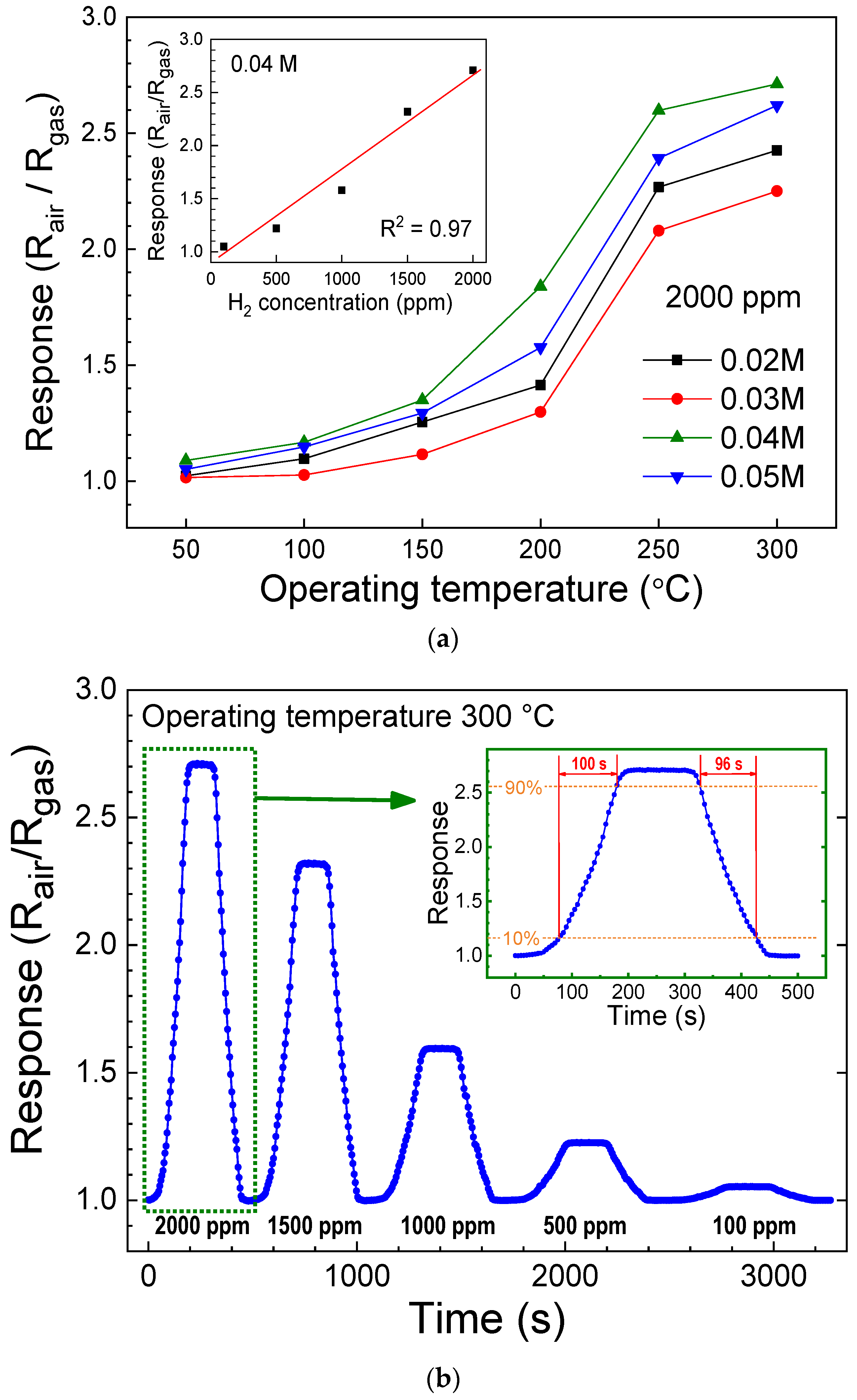


| Device | H2 Concentration (ppm) | Operating Temperature | Response (Sensitivity) | Response/Recovery Time | Reference |
|---|---|---|---|---|---|
| ZNA | 500 | 180 °C | |Ia − Ig|/Ia = 0.26 | -/- | [14] |
| ZnO with a MoS2 nanosheet catalyst | 100 | 250 °C | Ra/Rg~4 | 7 s/23 s | [30] |
| single ZnO NW | 100 | RT | |Ra − Rg|/R = 0.34 | 64 s/11 s | [34] |
| Pd nanoparticles-ZNA | 10,000 | RT | (Va − Vg)/Vg = 0.373 | 100 s/- | [35] |
| 1-D ZnO NWs | 250 | 300 °C | |Ga − Gg|/Gg = 1.66 | >300 s/>300 s | [38] |
| Ag-doped ZnO thin films | 1000 | 300 °C | |Ia − Ig|/Ia = 0.46 | >300 s/>300 s | [39] |
| Ag/Pd nanoparticle-ZnO nanoplates | 500 | 400 °C | Ra/Rg = 78 | 2 s/13 s | [40] |
| Pt nanoparticles-ZnO pencil-like microstructures | 100 | 150 °C | |Ra − Rg|/Ra = 0.638 | 193 s/378 s | [41] |
| Pd–ZnO nanosheets | 50 | 250 °C | Ra/Rg = 2.51 | 336 s/294 s | [42] |
| ZnO nanostructured thin film | 1200 | 400 °C | (Ra − Rg)/Ra = 0.23 | 110 s/- | [43] |
| ZNA on ZnO-AgNM layer | 2000 | 300 °C | Ra/Rg = 2.71 (Ra − Rg)/Ra = 0.631 | 100 s/96 s | This work |
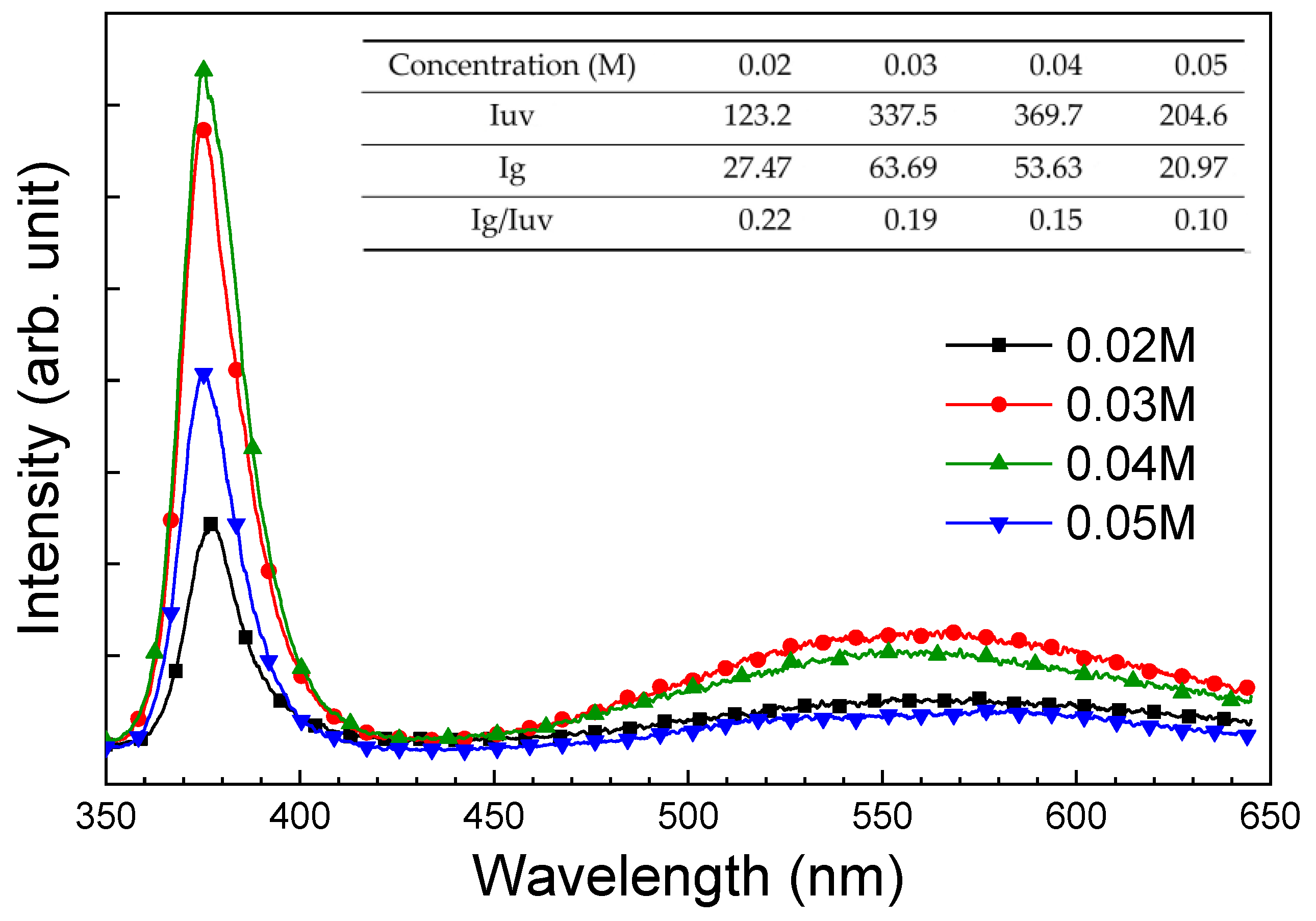
| Concentration (M) | 0.02 | 0.03 | 0.04 | 0.05 |
| RUV (A/W) | 1.29 | 6.95 | 4.53 × 101 | 1.14 × 10² |
| Rgreen (A/W) | 8.60 × 10⁻² | 6.30 × 10⁻² | 4.50 × 10⁻¹ | 5.62 × 10⁻¹ |
| Rred (A/W) | 3.15 × 10⁻⁶ | 1.23 × 10⁻⁴ | 1.57 × 10⁻⁴ | 1.57 × 10⁻⁴ |
| RUV/Rgreen | 1.50 × 10² | 1.10 × 10² | 1.01 × 10² | 2.03 × 10² |
| RUV/Rred | 4.10 × 10⁵ | 5.65 × 10⁴ | 2.89 × 10⁵ | 7.26 × 10⁵ |
| Detectivity (Jones) | 1.02 × 10¹³ | 5.02 × 10¹³ | 2.92 × 10¹⁴ | 6.37 × 10¹⁴ |
Disclaimer/Publisher’s Note: The statements, opinions and data contained in all publications are solely those of the individual author(s) and contributor(s) and not of MDPI and/or the editor(s). MDPI and/or the editor(s) disclaim responsibility for any injury to people or property resulting from any ideas, methods, instructions or products referred to in the content. |
© 2024 by the authors. Licensee MDPI, Basel, Switzerland. This article is an open access article distributed under the terms and conditions of the Creative Commons Attribution (CC BY) license (https://creativecommons.org/licenses/by/4.0/).
Share and Cite
Wang, F.-H.; Li, A.-J.; Liu, H.-W.; Kang, T.-K. One-Dimensional ZnO Nanorod Array Grown on Ag Nanowire Mesh/ZnO Composite Seed Layer for H2 Gas Sensing and UV Detection Applications. Sensors 2024, 24, 5852. https://doi.org/10.3390/s24175852
Wang F-H, Li A-J, Liu H-W, Kang T-K. One-Dimensional ZnO Nanorod Array Grown on Ag Nanowire Mesh/ZnO Composite Seed Layer for H2 Gas Sensing and UV Detection Applications. Sensors. 2024; 24(17):5852. https://doi.org/10.3390/s24175852
Chicago/Turabian StyleWang, Fang-Hsing, An-Jhe Li, Han-Wen Liu, and Tsung-Kuei Kang. 2024. "One-Dimensional ZnO Nanorod Array Grown on Ag Nanowire Mesh/ZnO Composite Seed Layer for H2 Gas Sensing and UV Detection Applications" Sensors 24, no. 17: 5852. https://doi.org/10.3390/s24175852