


Complementary Metal–Oxide–Semiconductor-Based Magnetic and Optical Sensors for Life Science Applications


Abstract
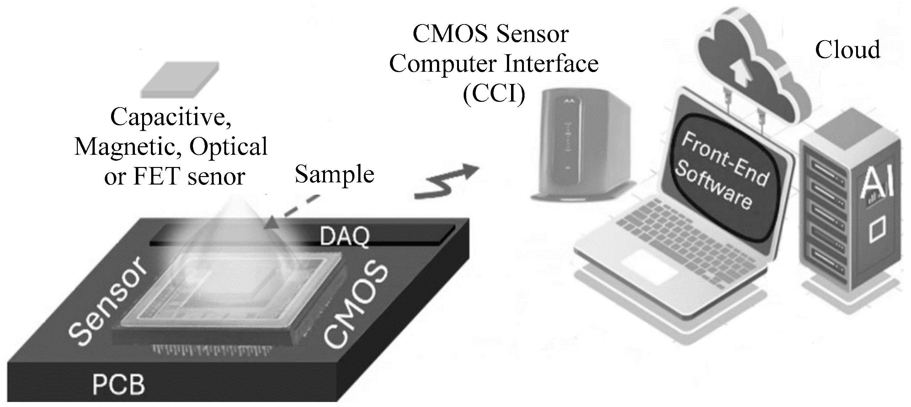
:1. Introduction
2. CMOS-Based Magnetic Sensors
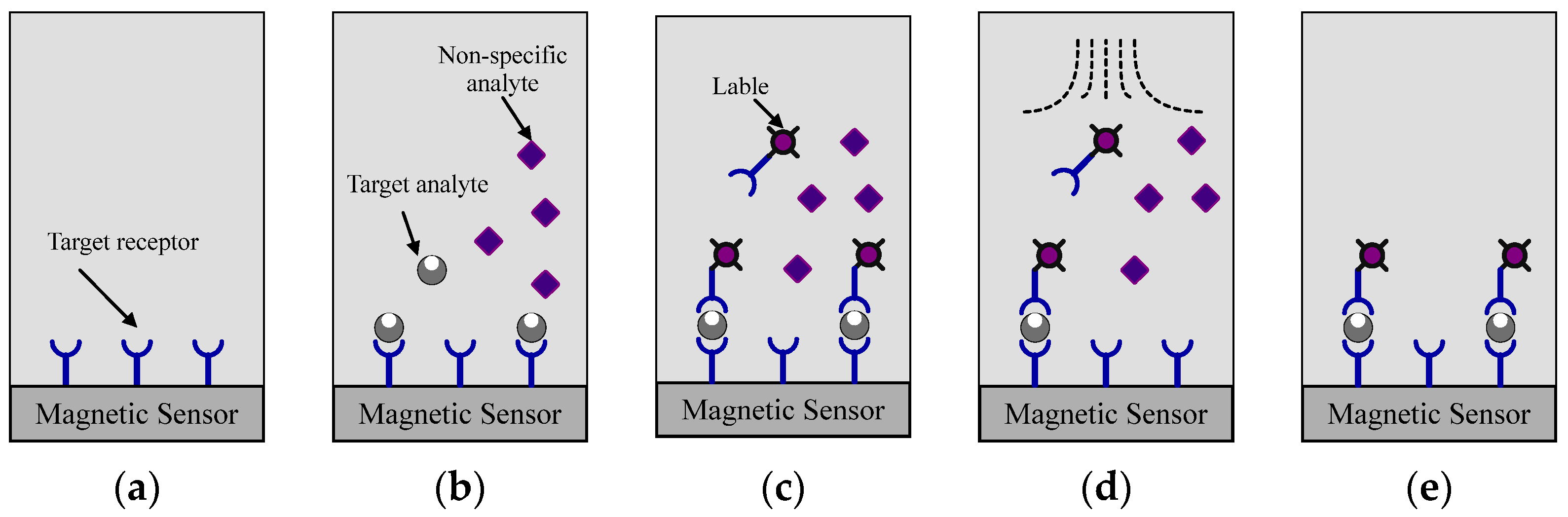
2.1. Sensing Principle of Magnetic Sensors
2.2. CMOS-Based Interface Circuit of Magnetic Sensors
2.2.1. Inductive Sensors
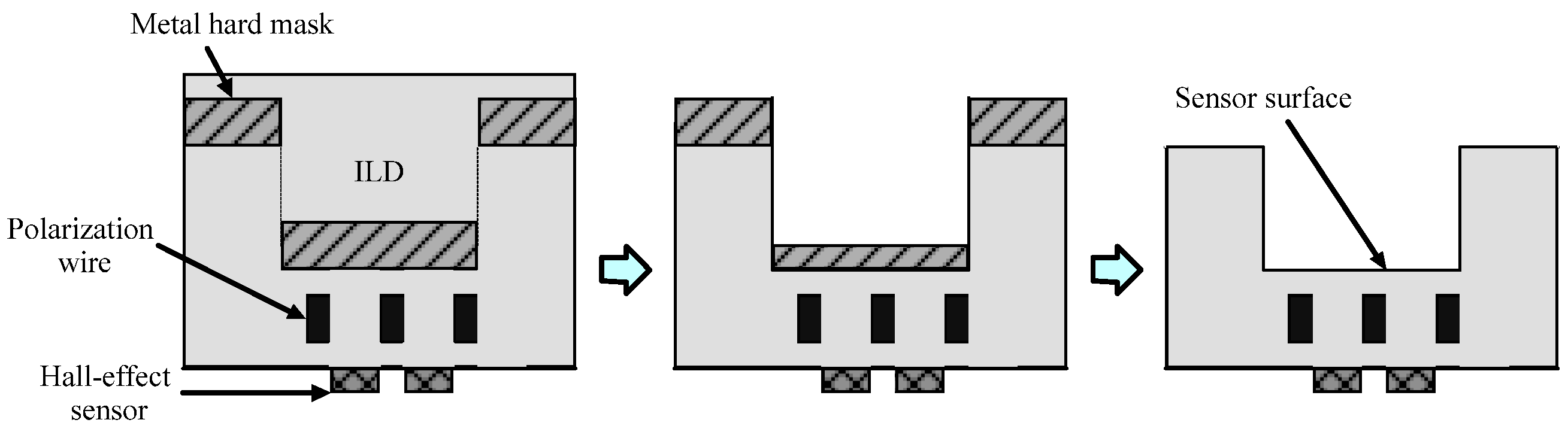
2.2.2. Hall Effect Sensors
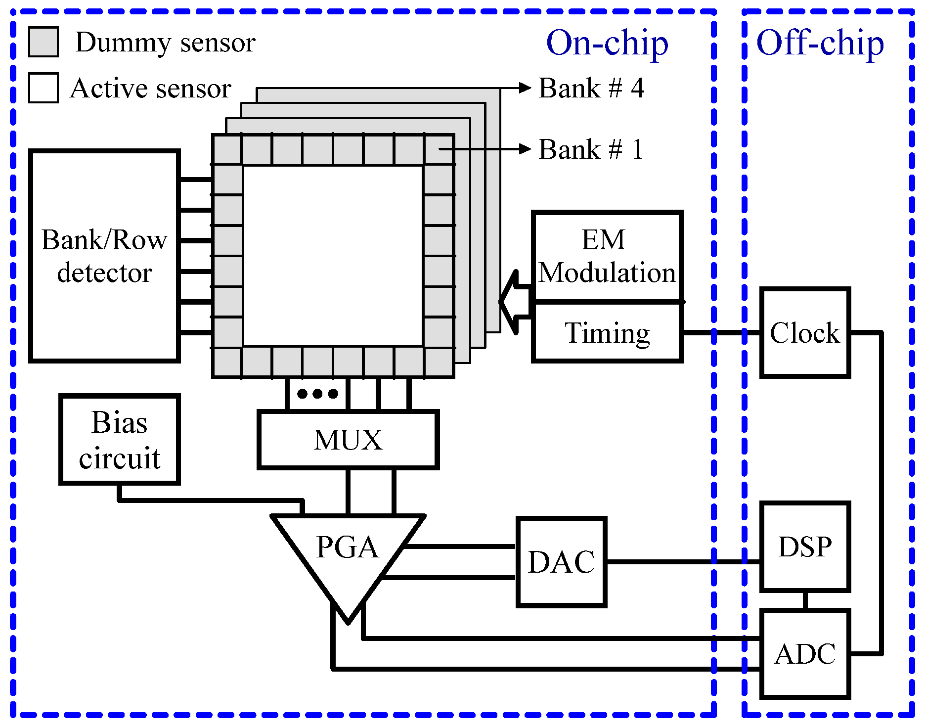
2.2.3. GMR Sensors
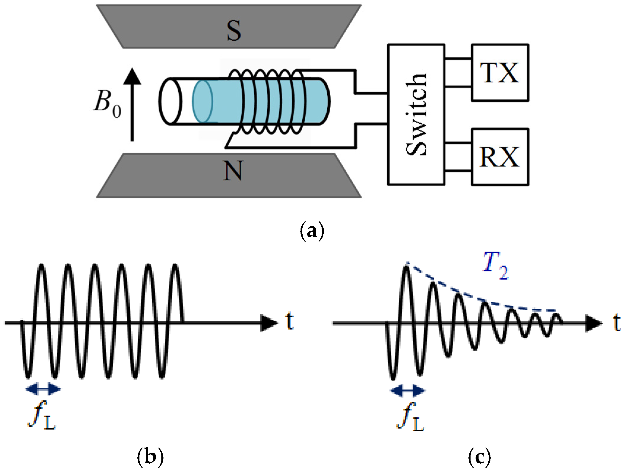
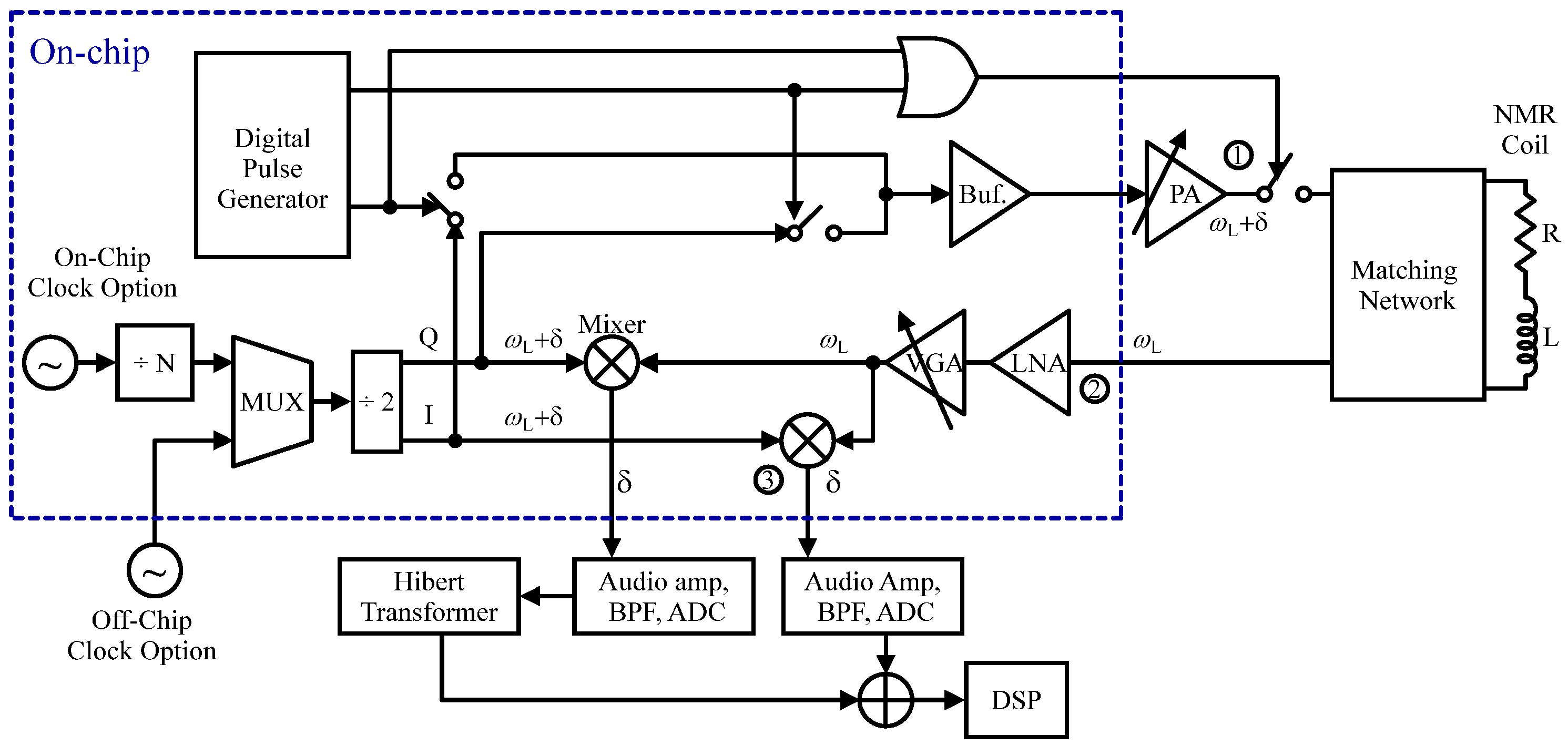
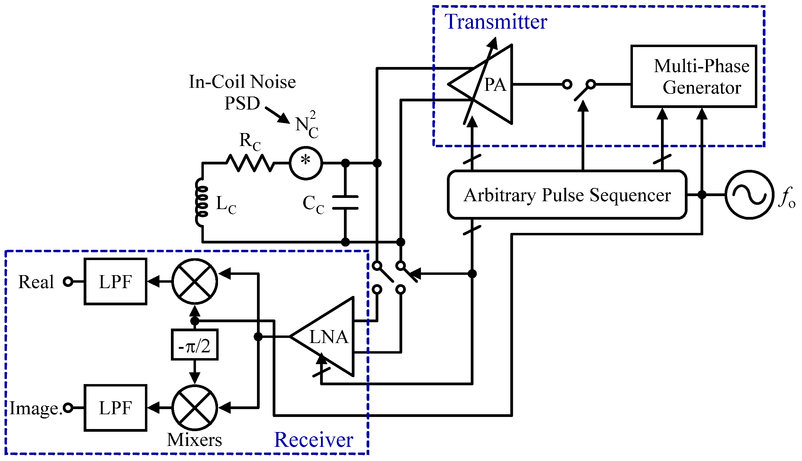
2.2.4. NMR Sensors
3. CMOS-Based Optical Sensors
3.1. Sensing Principle of Optical Sensors
3.2. CMOS-Based Interface Circuit of Optical Sensors
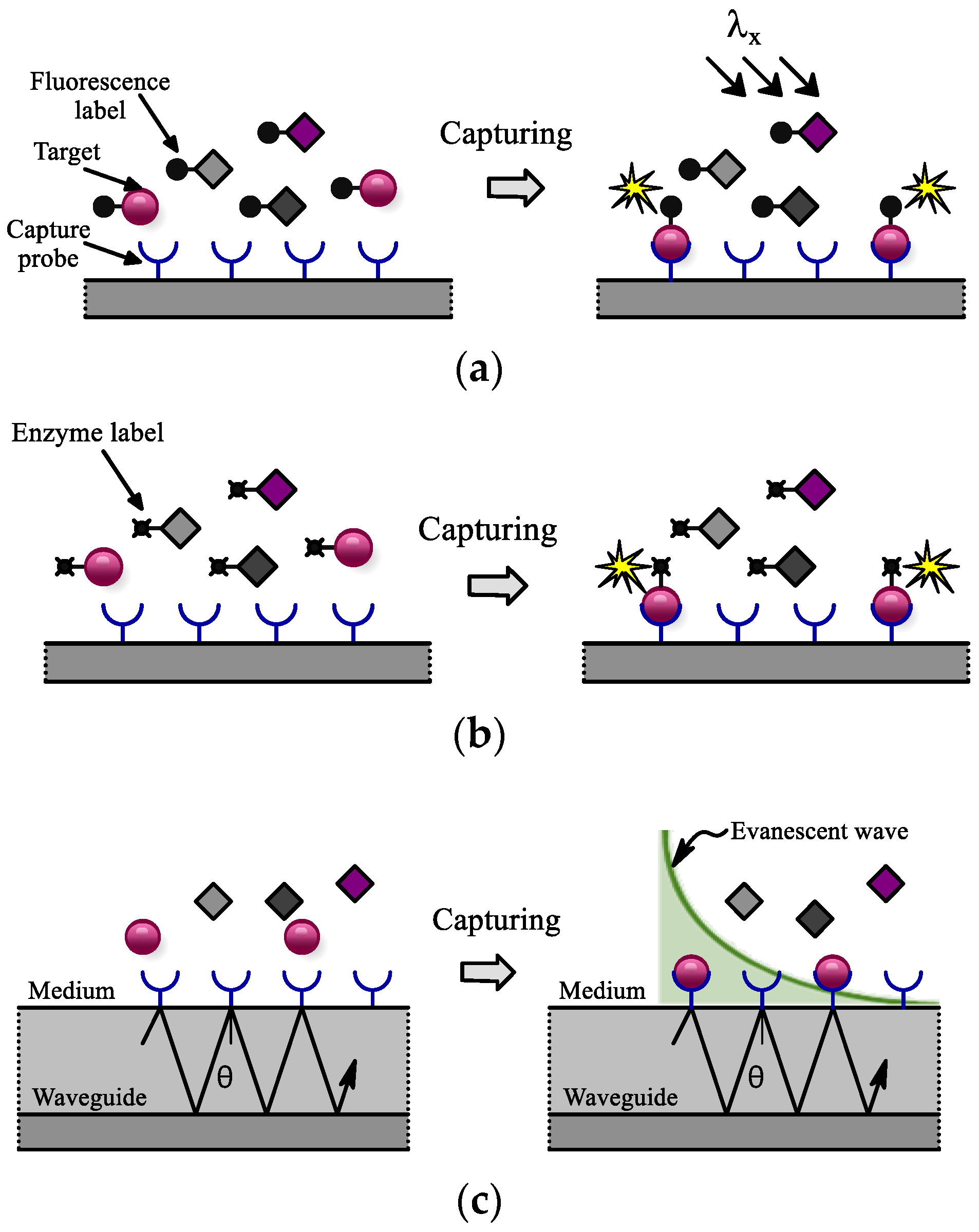
3.2.1. Fluorescence Sensors
3.2.2. Bioluminescence Sensors
3.2.3. Evanescent Wave Sensors
4. Conclusions and Future Remarks
Author Contributions
Funding
Conflicts of Interest
References
- Syu, Y.-C.; Hsu, W.-E.; Lin, C.-T. Field-effect transistor biosensing: Devices and clinical applications. ECS J. Solid State Sci. Technol. 2018, 7, Q3196. [Google Scholar] [CrossRef]
- Sadighbayan, D.; Hasanzadeh, M.; Ghafar-Zadeh, E. Biosensing based on field-effect transistors (FET): Recent progress and challenges. TrAC Trends Anal. Chem. 2020, 133, 116067. [Google Scholar] [CrossRef]
- Panahi, A.; Ghafar-Zadeh, E. Emerging Field-Effect Transistor Biosensors for Life Science Applications. Bioengineering 2023, 10, 793. [Google Scholar] [CrossRef]
- Ghafar-Zadeh, E.; Sawan, M.; Chodavarapu, V.P.; Hosseini-Nia, T. Bacteria growth monitoring through a differential CMOS capacitive sensor. IEEE Trans. Biomed. Circuits Syst. 2010, 4, 232–238. [Google Scholar] [CrossRef] [PubMed]
- Couniot, N.; Francis, L.A.; Flandre, D. A 16 × 16 CMOS capacitive biosensor array towards detection of single bacterial cell. IEEE Trans. Biomed. Circuits Syst. 2015, 10, 364–374. [Google Scholar] [CrossRef] [PubMed]
- Tabrizi, H.O.; Farhanieh, O.; Owen, Q.; Magierowski, S.; Ghafar-Zadeh, E. Wide input dynamic range fully integrated capacitive sensor for life science applications. IEEE Trans. Biomed. Circuits Syst. 2021, 15, 339–350. [Google Scholar] [CrossRef]
- Tabrizi, H.O.; Forouhi, S.; Azadmousavi, T.; Ghafar-Zadeh, E. A Multidisciplinary Approach toward CMOS Capacitive Sensor Array for Droplet Analysis. Micromachines 2024, 15, 232. [Google Scholar] [CrossRef]
- Lai, W.-A.; Lin, C.-H.; Yang, Y.-S.; Lu, M.S.-C. Ultrasensitive and label-free detection of pathogenic avian influenza DNA by using CMOS impedimetric sensors. Biosens. Bioelectron. 2012, 35, 456–460. [Google Scholar] [CrossRef]
- Lai, W.-A.; Lin, C.-H.; Yang, Y.-S.; Lu, M.S.-C. Ultrasensitive detection of avian influenza virus by using CMOS impedimetric sensor arrays. In Proceedings of the 2012 IEEE 25th International Conference on Micro Electro Mechanical Systems (MEMS), Paris, France, 29 January–2 February 2012; pp. 894–897. [Google Scholar]
- Nakazato, K. Potentiometric, amperometric, and impedimetric CMOS biosensor array. In State of the Art in Biosensors-General Aspects; IntechOpen: London, UK, 2013. [Google Scholar]
- Fan, V.L.S.; Yusof, Y. Design of fully integrated impedimetric CMOS biosensor for DNA detection. Int. J. Nanoelectron. Mater. 2015, 8, 55–60. [Google Scholar]
- Sun, N.; Yoon, T.-J.; Lee, H.; Andress, W.; Weissleder, R.; Ham, D. Palm NMR and 1-chip NMR. IEEE J. Solid-State Circuits 2010, 46, 342–352. [Google Scholar] [CrossRef]
- Manickam, A.; Singh, R.; McDermott, M.W.; Wood, N.; Bolouki, S.; Naraghi-Arani, P.; Johnson, K.A.; Kuimelis, R.G.; Schoolnik, G.; Hassibi, A. A fully integrated CMOS fluorescence biochip for DNA and RNA testing. IEEE J. Solid-State Circuits 2017, 52, 2857–2870. [Google Scholar] [CrossRef] [PubMed]
- Adamopoulos, C.; Zarkos, P.; Buchbinder, S.; Bhargava, P.; Niknejad, A.; Anwar, M.; Stojanovic, V. Lab-on-chip for everyone: Introducing an electronic-photonic platform for multiparametric biosensing using standard CMOS processes. IEEE Open J. Solid-State Circuits Soc. 2021, 1, 198–208. [Google Scholar] [CrossRef]
- Liu, Q.; Jimenez, M.; Inda, M.E.; Riaz, A.; Zirtiloglu, T.; Chandrakasan, A.P.; Lu, T.K.; Traverso, G.; Nadeau, P.; Yazicigil, R.T. A threshold-based bioluminescence detector with a CMOS-integrated photodiode array in 65 nm for a multi-diagnostic ingestible capsule. IEEE J. Solid-State Circuits 2022, 58, 838–851. [Google Scholar] [CrossRef]
- Aghimand, F.; Hu, C.; Sharma, S.; Pochana, K.K.; Murray, R.M.; Emami, A. 21.1 A 65nm CMOS Living-Cell Dynamic Fluorescence Sensor with 1.05 fA Sensitivity at 600/700 nm Wavelengths. In Proceedings of the 2023 IEEE International Solid-State Circuits Conference (ISSCC), San Francisco, CA, USA, 19–23 February 2023; pp. 312–314. [Google Scholar]
- Gambini, S.; Skucha, K.; Liu, P.P.; Kim, J.; Krigel, R. A 10 kPixel CMOS Hall sensor array with baseline suppression and parallel readout for immunoassays. IEEE J. Solid-State Circuits 2012, 48, 302–317. [Google Scholar] [CrossRef]
- Issadore, D.; Park, Y.I.; Shao, H.; Min, C.; Lee, K.; Liong, M.; Weissleder, R.; Lee, H. Magnetic sensing technology for molecular analyses. Lab Chip 2014, 14, 2385–2397. [Google Scholar] [CrossRef] [PubMed]
- Pourmodheji, H.; Ghafar-Zadeh, E.; Magierowski, S. Active nuclear magnetic resonance probe: A new multidiciplinary approach toward highly sensitive biomolecoular spectroscopy. In Proceedings of the 2015 IEEE International Symposium on Circuits and Systems (ISCAS), Lisbon, Portugal, 24–27 May 2015; pp. 473–476. [Google Scholar]
- Handwerker, J.; Pérez-Rodas, M.; Beyerlein, M.; Vincent, F.; Beck, A.; Freytag, N.; Yu, X.; Pohmann, R.; Anders, J.; Scheffler, K. A CMOS NMR needle for probing brain physiology with high spatial and temporal resolution. Nat. Methods 2020, 17, 64–67. [Google Scholar] [CrossRef]
- Zhou, X.; Mai, E.; Sveiven, M.; Pochet, C.; Jiang, H.; Huang, C.-C.; Hall, D.A. A 9.7-nTrms, 704-ms Magnetic Biosensor Front-End for Detecting Magneto-Relaxation. IEEE J. Solid-State Circuits 2021, 56, 2171–2181. [Google Scholar] [CrossRef]
- Lee, D.; Choi, K.-S.; Jiang, F.; Liu, H.; Jung, D.; Kong, Y.; Saif, M.; Huang, Z.; Wang, J.; Wang, H. 17.6 Fully Integrated CMOS Ferrofluidic Biomolecular Processing Platform with On-Chip Droplet-Based Manipulation, Mul-tiplexing and Sensing. In Proceedings of the 2024 IEEE International Solid-State Circuits Conference (ISSCC), San Francisco, CA, USA, 18–22 February 2024; pp. 324–326. [Google Scholar]
- Zhang, A.; Krüger, D.; Aghelnejad, B.; Yang, G.; Hinton, H.; Song, Y.-Q.; Ham, D. A Portable Wideband CMOS NMR Spectrometer for Multinuclear Molecular Fingerprinting. IEEE J. Solid-State Circuits 2024. early access. [Google Scholar] [CrossRef]
- Rothberg, J.M.; Hinz, W.; Rearick, T.M.; Schultz, J.; Mileski, W.; Davey, M.; Leamon, J.H.; Johnson, K.; Milgrew, M.J.; Edwards, M.; et al. An integrated semiconductor device enabling non-optical genome sequencing. Nature 2011, 475, 348–352. [Google Scholar] [CrossRef]
- Merriman, B.; Team, I.T.D.; Rothberg, J.M. Progress in ion torrent semiconductor chip based sequencing. Electrophoresis 2012, 33, 3397–3417. [Google Scholar] [CrossRef]
- Ghafar-Zadeh, E.; Sawan, M. A hybrid microfluidic/CMOS capacitive sensor dedicated to lab-on-chip applications. IEEE Trans. Biomed. Circuits Syst. 2007, 1, 270–277. [Google Scholar] [CrossRef] [PubMed]
- Nabovati, G.; Ghafar-Zadeh, E.; Letourneau, A.; Sawan, M. Towards High Throughput Cell Growth Screening: A New CMOS 8 × 8 Biosensor Array for Life Science Applications. IEEE Trans. Biomed. Circuits Syst. 2016, 11, 380–391. [Google Scholar] [CrossRef] [PubMed]
- Nabovati, G.; Ghafar-Zadeh, E.; Letourneau, A.; Sawan, M. Smart cell culture monitoring and drug test platform using CMOS capacitive sensor array. IEEE Trans. Biomed. Eng. 2018, 66, 1094–1104. [Google Scholar] [CrossRef] [PubMed]
- Forouhi, S.; Dehghani, R.; Ghafar-Zadeh, E. CMOS based capacitive sensors for life science applications: A review. Sens. Actuators A Phys. 2019, 297, 111531. [Google Scholar] [CrossRef]
- Mural, R.J.; Einstein, J.R.; Guan, X.; Mann, R.C.; Uberbacher, E.C. An artificial intelligence approach to DNA sequence feature recognition. Trends Biotechnol. 1992, 10, 66–69. [Google Scholar] [CrossRef]
- Al-Nima, R.R.O.; Al-Hatab, M.M.M.; Qasim, M.A. An Artificial Intelligence Approach for Verifying Persons by Employing the Deoxyribonucleic Acid (DNA) Nucleotides. J. Electr. Comput. Eng. 2023, 2023, 6678837. [Google Scholar] [CrossRef]
- Lin, L.; Cui, Z.; Wang, S.; Chen, Y.; Zong, Y. AI-driven Protein Engineering for DNA Sequence Modification. J. Theory Pract. Eng. Sci. 2024, 4, 183–190. [Google Scholar] [CrossRef]
- Vilhekar, R.S.; Rawekar, A. Artificial intelligence in genetics. Cureus 2024, 16, e52035. [Google Scholar] [CrossRef]
- Dheyab, H.F.; Ucan, O.N.; Khalaf, M.; Mohammed, A.H. Implementation a various types of machine learning approaches for biomedical datasets based on sickle cell disorder. In Proceedings of the 2020 4th International Symposium on Multidisciplinary Studies and Innovative Technologies (ISMSIT), Istanbul, Turkey, 22–24 October 2020; pp. 1–6. [Google Scholar]
- Bigorra, L.; Larriba, I.; Gutiérrez-Gallego, R. Machine learning algorithms for the detection of spurious white blood cell differentials due to erythrocyte lysis resistance. J. Clin. Pathol. 2019, 72, 431–437. [Google Scholar] [CrossRef]
- Ferdous, M.; Debnath, J.; Chakraborty, N.R. Machine learning algorithms in healthcare: A literature survey. In Proceedings of the 2020 11th International Conference on Computing, Communication and Networking Technologies (ICCCNT), Kharagpur, India, 1–3 July 2020; pp. 1–6. [Google Scholar]
- Patel, A.; Gan, K.; Li, A.A.; Weiss, J.; Nouraie, M.; Tayur, S.; Novelli, E.M. Machine-learning algorithms for predicting hospital re-admissions in sickle cell disease. Br. J. Haematol. 2021, 192, 158–170. [Google Scholar] [CrossRef]
- Razavi, B. CMOS technology characterization for analog and RF design. IEEE J. Solid-State Circuits 1999, 34, 268–276. [Google Scholar] [CrossRef]
- Arya, S.K.; Wong, C.C.; Jeon, Y.J.; Bansal, T.; Park, M.K. Advances in complementary-metal–oxide–semiconductor-based integrated biosensor arrays. Chem. Rev. 2015, 115, 5116–5158. [Google Scholar] [CrossRef] [PubMed]
- Iwai, H. Future of nano CMOS technology. Solid-State Electron. 2015, 112, 56–67. [Google Scholar] [CrossRef]
- Milgrew, M.; Hammond, P.; Cumming, D. The development of scalable sensor arrays using standard CMOS technology. Sens. Actuators B Chem. 2004, 103, 37–42. [Google Scholar] [CrossRef]
- Jang, B.; Hassibi, A. Biosensor systems in standard CMOS processes: Fact or fiction? IEEE Trans. Ind. Electron. 2009, 56, 979–985. [Google Scholar] [CrossRef]
- Lei, K.-M.; Mak, P.-I.; Law, M.-K.; Martins, R.P. CMOS biosensors for in vitro diagnosis–transducing mechanisms and applications. Lab Chip 2016, 16, 3664–3681. [Google Scholar] [CrossRef]
- Hassibi, A.; Wood, N.; Manickam, A. CMOS biochips: Challenges and opportunities. In Proceedings of the 2018 IEEE Custom Integrated Circuits Conference (CICC), San Diego, CA, USA, 8–11 April 2018; pp. 1–7. [Google Scholar]
- Forouhi, S.; Ghafar-Zadeh, E. Applications of CMOS devices for the diagnosis and control of infectious diseases. Micromachines 2020, 11, 1003. [Google Scholar] [CrossRef]
- DeBusschere, B.D.; Kovacs, G.T. Portable cell-based biosensor system using integrated CMOS cell-cartridges. Biosens. Bioelectron. 2001, 16, 543–556. [Google Scholar] [CrossRef]
- Hussain, A.M.; Hussain, M.M. CMOS-technology-enabled flexible and stretchable electronics for internet of everything applications. Adv. Mater. 2016, 28, 4219–4249. [Google Scholar] [CrossRef]
- Azadmousavi, T.; Aghdam, E.N.; Frounchi, J. A Power-Efficient Configurable FSK–OOK Transmitter with Scalable Data Rate for Wireless Medical Applications. Circuits Syst. Signal Process. 2020, 39, 2776–2795. [Google Scholar] [CrossRef]
- Liu, P.P.; Skucha, K.; Duan, Y.; Megens, M.; Kim, J.; Izyumin, I.I.; Gambini, S.; Boser, B. Magnetic relaxation detector for microbead labels. IEEE J. Solid-State Circuits 2012, 47, 1056–1064. [Google Scholar] [CrossRef] [PubMed]
- Olorocisimo, J.P.; Ohta, Y.; Regonia, P.R.; Castillo, V.C.; Yoshimoto, J.; Takehara, H.; Sasagawa, K.; Ohta, J. Brain-implantable needle-type CMOS imaging device enables multi-layer dissection of seizure calcium dynamics in the hippocampus. J. Neural Eng. 2024, 21, 046022. [Google Scholar] [CrossRef]
- Rabbani, R.; Roschelle, M.; Gweon, S.; Kumar, R.; Vercruysse, A.; Cho, N.W.; Spitzer, M.H.; Niknejad, A.M.; Stojanovic, V.M.; Anwar, M. 17.3 A Fully Wireless, Miniaturized, Multicolor Fluorescence Image Sensor Implant for Real-Time Monitoring in Cancer Therapy. In Proceedings of the 2024 IEEE International Solid-State Circuits Conference (ISSCC), San Francisco, CA, USA, 18–22 February 2024; pp. 318–320. [Google Scholar]
- Yu, Z.; Liao, H.-C.; Alrashdan, F.; Wen, Z.; Zou, Y.; Woods, J.; Wang, W.; Robinson, J.T.; Yang, K. 33.6 A Millimetric Batteryless Biosensing and Stimulating Implant with Magnetoelectric Power Transfer and 0.9 pJ/b PWM Backscatter. In Proceedings of the 2024 IEEE International Solid-State Circuits Conference (ISSCC), San Francisco, CA, USA, 18–22 February 2024; pp. 551–553. [Google Scholar]
- Kotitz, R.; Matz, H.; Trahms, L.; Koch, H.; Weitschies, W.; Rheinlander, T.; Semmler, W.; Bunte, T. SQUID based remanence measurements for immunoassays. IEEE Trans. Appl. Supercond. 1997, 7, 3678–3681. [Google Scholar] [CrossRef]
- Wang, H.; Chen, Y.; Hassibi, A.; Scherer, A.; Hajimiri, A. A frequency-shift CMOS magnetic biosensor array with single-bead sensitivity and no external magnet. In Proceedings of the Solid-State Circuits Conference-Digest of Technical Papers, San Francisco, CA, USA, 8–12 February 2009; ISSCC 2009. IEEE International: New York, NY, USA, 2009; pp. 438–439, 439a. [Google Scholar]
- Wang, H.; Kosai, S.; Sideris, C.; Hajimiri, A. An ultrasensitive CMOS magnetic biosensor array with correlated double counting noise suppression. In Proceedings of the 2010 IEEE MTT-S International Microwave Symposium, Anaheim, CA, USA, 23–28 May 2010; IEEE: New York, NY, USA, 2010; pp. 616–619. [Google Scholar]
- Wang, H.; Sideris, C.; Hajimiri, A. A frequency-shift based CMOS magnetic biosensor with spatially uniform sensor transducer gain. In Proceedings of the IEEE Custom Integrated Circuits Conference 2010, San Jose, CA, USA, 19–22 September 2010; IEEE: New York, NY, USA, 2010; pp. 1–4. [Google Scholar]
- Geng, J.; Zhang, L.; Zhu, C.; Dai, L.; Shi, X.; Qian, H. An oscillator-based CMOS magnetosensitive microarray biochip with on-chip inductor optimization methodology. IEEE Trans. Microw. Theory Tech. 2018, 66, 2556–2569. [Google Scholar] [CrossRef]
- Wang, H.; Mahdavi, A.; Tirrell, D.A.; Hajimiri, A. A magnetic cell-based sensor. Lab Chip 2012, 12, 4465–4471. [Google Scholar] [CrossRef]
- Pai, A.; Khachaturian, A.; Chapman, S.; Hu, A.; Wang, H.; Hajimiri, A. A handheld magnetic sensing platform for antigen and nucleic acid detection. Analyst 2014, 139, 1403–1411. [Google Scholar] [CrossRef] [PubMed]
- Sideris, C.; Hajimiri, A. Design and implementation of an integrated magnetic spectrometer for multiplexed biosensing. IEEE Trans. Biomed. Circuits Syst. 2013, 7, 773–784. [Google Scholar] [CrossRef]
- Fannin, P.; Cohen-Tannoudji, L.; Bertrand, E.; Giannitsis, A.; Oireachtaigh, C.M.; Bibette, J. Investigation of the complex susceptibility of magnetic beads containing maghemite nanoparticles. J. Magn. Magn. Mater. 2006, 303, 147–152. [Google Scholar] [CrossRef]
- Azadmousavi, T.; Ghafar-Zadeh, E. Design and Analysis of a Low-Voltage VCO: Reliability and Variability Performance. Micromachines 2023, 14, 2118. [Google Scholar] [CrossRef]
- Sideris, C.; Khial, P.P.; Hajimiri, A. Design and implementation of reference-free drift-cancelling CMOS magnetic sensors for biosensing applications. IEEE J. Solid-State Circuits 2018, 53, 3065–3075. [Google Scholar] [CrossRef]
- Azadmousavi, T.; Aghdam, E.N. A low power current-reuse LC-VCO with an adaptive body-biasing technique. AEU-Int. J. Electron. Commun. 2018, 89, 56–61. [Google Scholar] [CrossRef]
- Murali, P.; Niknejad, A.M.; Boser, B.E. CMOS microflow cytometer for magnetic label detection and classification. IEEE J. Solid-State Circuits 2016, 52, 543–555. [Google Scholar] [CrossRef]
- Gal-Katziri, M.; Hajimiri, A. Analysis and design of coupled inductive bridges for magnetic sensing applications. IEEE J. Solid-State Circuits 2019, 54, 1883–1894. [Google Scholar] [CrossRef]
- Hall, E.H. On a new action of the magnet on electric currents. Am. J. Math. 1879, 2, 287–292. [Google Scholar] [CrossRef]
- Besse, P.-A.; Boero, G.; Demierre, M.; Pott, V.; Popovic, R. Detection of a single magnetic microbead using a miniaturized silicon Hall sensor. Appl. Phys. Lett. 2002, 80, 4199–4201. [Google Scholar] [CrossRef]
- Wang, H. Magnetic sensors for diagnostic medicine: CMOS-based magnetic particle detectors for medical diagnosis applications. IEEE Microw. Mag. 2013, 14, 110–130. [Google Scholar] [CrossRef]
- Skucha, K.; Liu, P.; Megens, M.; Kim, J.; Boser, B. A compact Hall-effect sensor array for the detection and imaging of single magnetic beads in biomedical assays. In Proceedings of the 2011 16th International Solid-State Sensors, Actuators and Microsystems Conference, Beijing, China, 5–9 June 2011; IEEE: New York, NY, USA, 2011; pp. 1833–1836. [Google Scholar]
- Skucha, K.; Gambini, S.; Liu, P.; Megens, M.; Kim, J.; Boser, B. Design considerations for CMOS-integrated Hall-effect magnetic bead detectors for biosensor applications. J. Microelectromech. Syst. 2013, 22, 1327–1338. [Google Scholar] [CrossRef]
- Liu, P.; Skucha, K.; Megens, M.; Boser, B. A CMOS Hall-effect sensor for the characterization and detection of magnetic nanoparticles for biomedical applications. IEEE Trans. Magn. 2011, 47, 3449–3451. [Google Scholar] [CrossRef] [PubMed]
- Zou, H.; Lei, K.-M.; Martins, R.P.; Mak, P.-I. A CMOS Hall Sensors Array With Integrated Readout Circuit Resilient to Local Magnetic Interference From Current-Carrying Traces. IEEE Sens. J. 2023, 23, 16145–16153. [Google Scholar] [CrossRef]
- Bhalla, N.; Chung, D.W.Y.; Chang, Y.-J.; Uy, K.J.S.; Ye, Y.Y.; Chin, T.-Y.; Yang, H.C.; Pijanowska, D.G. Microfluidic platform for enzyme-linked and magnetic particle-based immunoassay. Micromachines 2013, 4, 257–271. [Google Scholar] [CrossRef]
- Kuo, P.-H.; Kuo, J.-C.; Hsueh, H.-T.; Hsieh, J.-Y.; Huang, Y.-C.; Wang, T.; Lin, Y.H.; Lin, C.T.; Yang, Y.J.; Lu, S.S. A smart CMOS assay SoC for rapid blood screening test of risk prediction. IEEE Trans. Biomed. Circuits Syst. 2015, 9, 790–800. [Google Scholar] [CrossRef] [PubMed]
- Seto, A.; Kusaka, C.; Nakazato, S.; Sato, T.; Hisamitsu, T.; Takeshige, C. Detection of extraordinary large bio-magnetic field strength from human hand during external Qi emission. Acupunct. Electro-Ther. Res. 1992, 17, 75–94. [Google Scholar] [CrossRef] [PubMed]
- Hisamitsu, T.; Seto, A.; Nakazato, S.; Yamamoto, T.; Aung, S.K. Emission of extremely strong magnetic fields from the head and whole body during oriental breathing exercises. Acupunct. Electro-Ther. Res. 1996, 21, 219–227. [Google Scholar] [CrossRef]
- Ignatov, I.; Mosin, O.; Niggli, H.; Drossinakis, C. Evaluating Possible Methods and Approaches for Registering of Electromagnetic Waves Emitted from the Human Body. Adv. Phys. Theor. Appl. 2014, 30, 15–33. [Google Scholar]
- Chang, T.; Juang, K.-C. CMOS hall sensor with reduced sensitivity drift by synchronous excitation calibration for wearable biomagnetic sensor in system-on-chip. In Proceedings of the 2016 IEEE SENSORS, Orlando, FL, USA, 30 October–3 November 2016; pp. 1–3. [Google Scholar]
- Heidari, H.; Zuo, S.; Krasoulis, A.; Nazarpour, K. CMOS magnetic sensors for wearable magnetomyography. In Proceedings of the 2018 40th Annual International Conference of the IEEE Engineering in Medicine and Biology Society (EMBC), Honolulu, HI, USA, 18–21 July 2018; pp. 2116–2119. [Google Scholar]
- Hardman, U. Magnetic Thin Film and Multilayer Systems: Physics, Analysis and Industrial Applications; Springer Series in Material Science; Springer: Cham, Switzerland, 1996. [Google Scholar]
- Graham, D.L.; Ferreira, H.A.; Freitas, P.P. Magnetoresistive-based biosensors and biochips. TRENDS Biotechnol. 2004, 22, 455–462. [Google Scholar] [CrossRef]
- Han, S.-J.; Yu, H.; Murmann, B.; Pourmand, N.; Wang, S.X. A high-density magnetoresistive biosensor array with drift-compensation mechanism. In Proceedings of the 2007 IEEE International Solid-State Circuits Conference, San Francisco, CA, USA, 11–15 February 2007; Digest of Technical Papers. IEEE: New York, NY, USA, 2007; pp. 168–594. [Google Scholar]
- Wang, S.X.; Li, G. Advances in giant magnetoresistance biosensors with magnetic nanoparticle tags: Review and outlook. IEEE Trans. Magn. 2008, 44, 1687–1702. [Google Scholar] [CrossRef]
- Hall, D.A.; Gaster, R.S.; Makinwa, K.A.A.; Wang, S.X.; Murmann, B. A 256 pixel magnetoresistive biosensor microarray in 0.18 µm CMOS. IEEE J. Solid-State Circuits 2013, 48, 1290–1301. [Google Scholar] [CrossRef]
- Zhou, X.; Huang, C.-C.; Hall, D.A. Giant magnetoresistive biosensor array for detecting magnetorelaxation. IEEE Trans. Biomed. Circuits Syst. 2017, 11, 755–764. [Google Scholar] [CrossRef]
- Zhou, X.; Sveiven, M.; Hall, D.A. 11.4 a fast-readout mismatch-insensitive magnetoresistive biosensor front-end achieving sub-ppm sensitivity. In Proceedings of the 2019 IEEE International Solid-State Circuits Conference-(ISSCC), San Francisco, CA, USA, 17–21 February 2019; IEEE: New York, NY, USA, 2019; pp. 196–198. [Google Scholar]
- Zhou, X. Magnetoresistive Biosensor Circuits and Systems for Ultrasensitive Point-of-Care Diagnostics. Ph.D. Thesis, University of California, San Diego, CA, USA, 2020. [Google Scholar]
- Han, S.-J.; Xu, L.; Yu, H.; Wilson, R.J.; White, R.L.; Pourmand, N.; Wang, S.X. CMOS integrated DNA microarray based on GMR sensors. In Proceedings of the 2006 International Electron Devices Meeting, San Francisco, CA, USA, 11–13 December 2006; IEEE: New York, NY, USA, 2006; pp. 1–4. [Google Scholar]
- Costa, T.; Cardoso, F.A.; Germano, J.; Freitas, P.P.; Piedade, M.S. A CMOS front-end with integrated magnetoresistive sensors for biomolecular recognition detection applications. IEEE Trans. Biomed. Circuits Syst. 2017, 11, 988–1000. [Google Scholar] [CrossRef]
- Huang, C.-C.; Zhou, X.; Hall, D.A. Giant magnetoresistive biosensors for time-domain magnetorelaxometry: A theoretical investigation and progress toward an immunoassay. Sci. Rep. 2017, 7, srep45493. [Google Scholar] [CrossRef]
- Adolphi, N.L.; Huber, D.L.; Jaetao, J.E.; Bryant, H.C.; Lovato, D.M.; Fegan, D.L.; Venturini, E.L.; Monson, T.C.; Tessier, T.E.; Hathaway, H.J.; et al. Characterization of magnetite nanoparticles for SQUID-relaxometry and magnetic needle biopsy. J. Magn. Magn. Mater. 2009, 321, 1459–1464. [Google Scholar] [CrossRef] [PubMed]
- Zhou, X.; Sveiven, M.; Hall, D.A. A CMOS magnetoresistive sensor front-end with mismatch-tolerance and sub-ppm sensitivity for magnetic immunoassays. IEEE Trans. Biomed. Circuits Syst. 2019, 13, 1254–1263. [Google Scholar] [CrossRef] [PubMed]
- Kim, K.; Hall, D.A.; Yao, C.; Lee, J.-R.; Ooi, C.C.; Bechstein, D.J.B.; Guo, Y.; Wang, S.X. Magnetoresistive biosensors with on-chip pulsed excitation and magnetic correlated double sampling. Sci. Rep. 2018, 8, 16493. [Google Scholar] [CrossRef] [PubMed]
- Perez, J.M.; Josephson, L.; O’Loughlin, T.; Högemann, D.; Weissleder, R. Magnetic relaxation switches capable of sensing molecular interactions. Nat. Biotechnol. 2002, 20, 816–820. [Google Scholar] [CrossRef] [PubMed]
- Lee, H.; Sun, E.; Ham, D.; Weissleder, R. Chip–NMR biosensor for detection and molecular analysis of cells. Nat. Med. 2008, 14, 869–874. [Google Scholar] [CrossRef]
- Sun, N.; Liu, Y.; Lee, H.; Weissleder, R.; Ham, D. CMOS RF biosensor utilizing nuclear magnetic resonance. IEEE J. Solid-State Circuits 2009, 44, 1629–1643. [Google Scholar] [CrossRef]
- Lei, K.-M.; Heidari, H.; Mak, P.-I.; Law, M.-K.; Maloberti, F.; Martins, R.P. A handheld high-sensitivity micro-NMR CMOS platform with B-field stabilization for multi-type biological/chemical assays. IEEE J. Solid-State Circuits 2016, 52, 284–297. [Google Scholar] [CrossRef]
- Srinivasan, V.; Pamula, V.K.; Fair, R.B. An integrated digital microfluidic lab-on-a-chip for clinical diagnostics on human physiological fluids. Lab Chip 2004, 4, 310–315. [Google Scholar] [CrossRef] [PubMed]
- Barbulovic-Nad, I.; Yang, H.; Park, P.S.; Wheeler, A.R. Digital microfluidics for cell-based assays. Lab Chip 2008, 8, 519–526. [Google Scholar] [CrossRef]
- Lei, K.-M.; Mak, P.-I.; Law, M.-K.; Martins, R.P. A uNMR CMOS Transceiver Using a Butterfly-Coil Input for Integration With a Digital Microfluidic Device Inside a Portable Magnet. IEEE J. Solid-State Circuits 2016, 51, 2274–2286. [Google Scholar] [CrossRef]
- Kim, J.; Hammer, B.; Harjani, R. A 5–300MHz CMOS transceiver for multi-nuclear NMR spectroscopy. In Proceedings of the IEEE 2012 Custom Integrated Circuits Conference, San Jose, CA, USA, 9–12 September 2012; pp. 1–4. [Google Scholar]
- Ha, D.; Paulsen, J.; Sun, N.; Song, Y.-Q.; Ham, D. Scalable NMR spectroscopy with semiconductor chips. Proc. Natl. Acad. Sci. USA 2014, 111, 11955–11960. [Google Scholar] [CrossRef] [PubMed]
- Anders, J.; Chiaramonte, G.; SanGiorgio, P.; Boero, G. A single-chip array of NMR receivers. J. Magn. Reson. 2009, 201, 239–249. [Google Scholar] [CrossRef] [PubMed]
- Pourmodheji, H.; Ghafar-Zadeh, E.; Magierowski, S. A CMOS differential receiver dedicated to nuclear magnetic resonance applications. Analog Integr. Circuits Signal Process. 2017, 91, 97–109. [Google Scholar] [CrossRef]
- Grisi, M.; Gualco, G.; Boero, G. A broadband single-chip transceiver for multi-nuclear NMR probes. Rev. Sci. Instrum. 2015, 86, 044703. [Google Scholar] [CrossRef]
- Lei, K.-M.; Ha, D.; Song, Y.-Q.; Westervelt, R.M.; Martins, R.; Mak, P.-I.; Ham, D. Portable NMR with parallelism. Anal. Chem. 2020, 92, 2112–2120. [Google Scholar] [CrossRef]
- Sporrer, B.; Wu, L.; Bettini, L.; Vogt, C.; Reber, J.; Marjanovic, J.; Burger, T.; Brunner, D.O.; Pruessmann, K.P.; Troster, G.; et al. A fully integrated dual-channel on-coil CMOS receiver for array coils in 1.5–10.5 T MRI. IEEE Trans. Biomed. Circuits Syst. 2017, 11, 1245–1255. [Google Scholar] [CrossRef]
- Jang, B.; Cao, P.; Chevalier, A.; Ellington, A.; Hassibi, A. A CMOS fluorescent-based biosensor microarray. In Proceedings of the 2009 IEEE International Solid-State Circuits Conference-Digest of Technical Papers, San Francisco, CA, USA, 8–12 February 2009; IEEE: New York, NY, USA, 2009; pp. 436–437. [Google Scholar]
- Hong, L.; Li, H.; Yang, H.; Sengupta, K. Fully integrated fluorescence biosensors on-chip employing multi-functional nanoplasmonic optical structures in CMOS. IEEE J. Solid-State Circuits 2017, 52, 2388–2406. [Google Scholar] [CrossRef]
- Aghlmand, F.; Hu, C.Y.; Sharma, S.; Pochana, K.; Murray, R.M.; Emami, A. A 65-nm CMOS Fluorescence Sensor for Dynamic Monitoring of Living Cells. IEEE J. Solid-State Circuits 2023, 58, 3003–3019. [Google Scholar] [CrossRef]
- Khiarak, M.N.; Martel, S.; De Koninck, Y.; Gosselin, B. A high-sensitivity CMOS biophotometry sensor with embedded continuous-time ΣΔ modulation. In Proceedings of the 2017 IEEE International Symposium on Circuits and Systems (ISCAS), Baltimore, MD, USA, 28–31 May 2017; pp. 1–4. [Google Scholar]
- Kobayashi, T.; Haruta, M.; Sasagawa, K.; Matsumata, M.; Eizumi, K.; Kitsumoto, C.; Motoyama, M.; Maezawa, Y.; Ohta, Y.; Noda, T.; et al. Optical communication with brain cells by means of an implanted duplex micro-device with optogenetics and Ca2+ fluoroimaging. Sci. Rep. 2016, 6, 21247. [Google Scholar] [CrossRef]
- Rabbani, R.; Najafiaghdam, H.; Zhao, B.; Zeng, M.; Stojanovic, V.; Muller, R.; Anwar, M. A 36 × 40 Wireless Fluorescence Image Sensor for Real-Time Microscopy in Cancer Therapy. In Proceedings of the 2022 IEEE Custom Integrated Circuits Conference (CICC), Newport Beach, CA, USA, 24–27 April 2022; pp. 1–2. [Google Scholar]
- Zhu, C.; Hong, L.; Yang, H.; Sengupta, K. A packaged multiplexed fluorescent biomolecular sensor array and ultralow-power wireless interface in CMOS for ingestible electronic applications. IEEE Sens. J. 2022, 22, 24060–24074. [Google Scholar] [CrossRef]
- Van Dyke, K.; Van Dyke, C.; Woodfork, K. Luminescence Biotechnology: Instruments and Applications; CRC Press: Boca Raton, FL, USA, 2001. [Google Scholar]
- Eltoukhy, H.; Salama, K.; El Gamal, A.; Ronaghi, M.; Davis, R. A 0.18 µm CMOS 10−6 lux bioluminescence detection system-on-chip. In Proceedings of the 2004 IEEE International Solid-State Circuits Conference, San Francisco, CA, USA, 15–19 February 2004; pp. 222–223. [Google Scholar]
- Eltoukhy, H.; Salama, K.; Gamal, A.E. A 0.18 um CMOS bioluminescence detection lab-on-chip. IEEE J. Solid-State Circuits 2006, 41, 651–662. [Google Scholar] [CrossRef]
- Agah, A.; Vleugels, K.; Griffin, P.B.; Ronaghi, M.; Plummer, J.D.; Wooley, B.A. A High-Resolution Low-Power Incremental ΣΔ ADC With Extended Range for Biosensor Arrays. IEEE J. Solid-State Circuits 2010, 45, 1099–1110. [Google Scholar] [CrossRef]
- Agah, A.; Hassibi, A.; Plummer, J.D.; Griffin, P.B. Design requirements for integrated biosensor arrays. In Proceedings of the Imaging, Manipulation, and Analysis of Biomolecules and Cells: Fundamentals and Applications III, San Jose, CA, USA, 24–27 January 2005; pp. 403–413. [Google Scholar]
- Awan, M.A.; Ahmad, K.; Bermak, A.; Biswas, K.H.; Wang, B. An Asynchronous CMOS Current Readout With 124 dB Dynamic Range for Bioluminescence Sensing. IEEE Solid-State Circuits Lett. 2024, 7, 223–226. [Google Scholar] [CrossRef]
- Islam, S.K.; Vijayaraghavan, R.; Zhang, M.; Ripp, S.; Caylor, S.D.; Weathers, B.; Moser, S.; Terry, S.; Blalock, B.J.; Sayler, G.S. Integrated circuit biosensors using living whole-cell bioreporters. IEEE Trans. Circuits Syst. I Regul. Pap. 2007, 54, 89–98. [Google Scholar] [CrossRef]
- Nadeau, P.; Mimee, M.; Carim, S.; Lu, T.K.; Chandrakasan, A.P. 21.1 Nanowatt circuit interface to whole-cell bacterial sensors. In Proceedings of the 2017 IEEE International Solid-State Circuits Conference (ISSCC), San Francisco, CA, USA, 5–9 February 2017; pp. 352–353. [Google Scholar]
- Adamopoulos, C.; Stojanovic, V. A Fully Integrated Electronic-Photonic Platform for Label-Free Biosensing; University of California at Berkeley: Berkeley, CA, USA, 2020. [Google Scholar]
- Sajan, S.C.; Singh, A.; Sharma, P.K.; Kumar, S. Silicon photonics biosensors for cancer cells detection—A review. IEEE Sens. J. 2023, 23, 3366–3377. [Google Scholar] [CrossRef]
- Shekhar, S.; Bogaerts, W.; Chrostowski, L.; Bowers, J.E.; Hochberg, M.; Soref, R.; Shastri, B.J. Roadmapping the next generation of silicon photonics. Nat. Commun. 2024, 15, 751. [Google Scholar] [CrossRef] [PubMed]
- Adamopoulos, C.; Buchbinder, S.; Zarkos, P.; Bhargava, P.; Gharia, A.; Ninkejad, A.; Anwar, M.; Stojanovic, V. Fully integrated electronic-photonic sensor for label-free refractive index sensing in advanced zero-change CMOS-SOI process. In Proceedings of the 2021 IEEE Custom Integrated Circuits Conference (CICC), Austin, TX, USA, 25–30 April 2021; pp. 1–2. [Google Scholar]
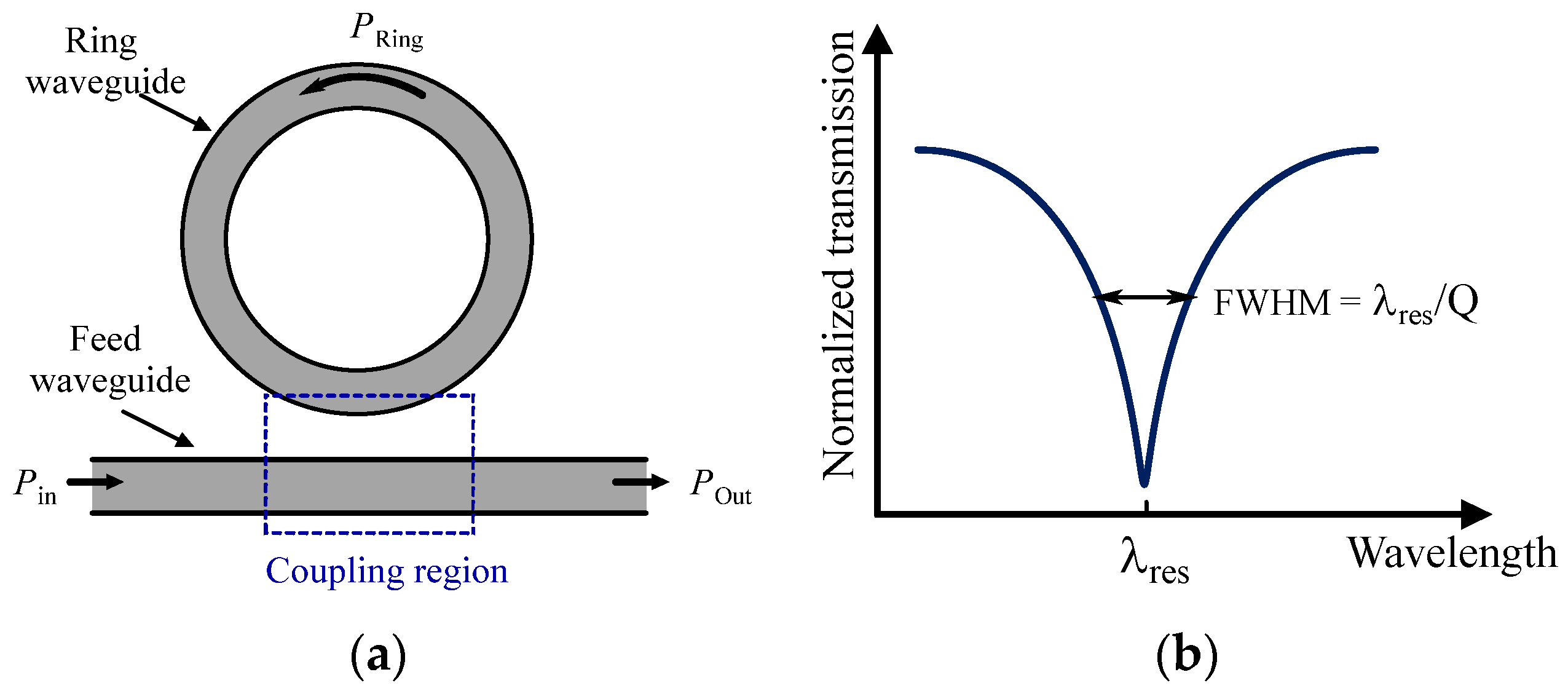
- Steglich, P.; Rabus, D.G.; Sada, C.; Paul, M.; Weller, M.G.; Mai, C.; Mai, A. Silicon Photonic Micro-Ring Resonators for Chemical and Biological Sensing: A Tutorial. IEEE Sensors J. 2021, 22, 10089–10105. [Google Scholar] [CrossRef]
- Zhang, H.; Lv, X.; Huang, B.; Cheng, C.; Zhang, Z.; Zhang, Z.; Fang, W.; Zhang, H.; Chen, R.; Huang, Y.; et al. In Situ Regeneration of Silicon Microring Biosensors Coated with Parylene C. Langmuir 2021, 38, 504–513. [Google Scholar] [CrossRef]
- Panda, S. Readout and Data Analysis Circuits for Silicon Photonic Evanescent Field Biosensors. Ph.D. Thesis, University of British Columbia, Vancouver, BC, Canada, 2024. [Google Scholar]


Disclaimer/Publisher’s Note: The statements, opinions and data contained in all publications are solely those of the individual author(s) and contributor(s) and not of MDPI and/or the editor(s). MDPI and/or the editor(s) disclaim responsibility for any injury to people or property resulting from any ideas, methods, instructions or products referred to in the content. |
© 2024 by the authors. Licensee MDPI, Basel, Switzerland. This article is an open access article distributed under the terms and conditions of the Creative Commons Attribution (CC BY) license (https://creativecommons.org/licenses/by/4.0/).
Share and Cite
Azadmousavi, T.; Ghafar-Zadeh, E. Complementary Metal–Oxide–Semiconductor-Based Magnetic and Optical Sensors for Life Science Applications. Sensors 2024, 24, 6264. https://doi.org/10.3390/s24196264
Azadmousavi T, Ghafar-Zadeh E. Complementary Metal–Oxide–Semiconductor-Based Magnetic and Optical Sensors for Life Science Applications. Sensors. 2024; 24(19):6264. https://doi.org/10.3390/s24196264
Chicago/Turabian StyleAzadmousavi, Tayebeh, and Ebrahim Ghafar-Zadeh. 2024. "Complementary Metal–Oxide–Semiconductor-Based Magnetic and Optical Sensors for Life Science Applications" Sensors 24, no. 19: 6264. https://doi.org/10.3390/s24196264