


A 60 GHz Class-C Wide Tuning-Range Two-Core VCO Utilizing a Gain-Boosting Frequency Doubling Technique and an Adaptive Bias Scheme for Robust Startup


Abstract
1. Introduction
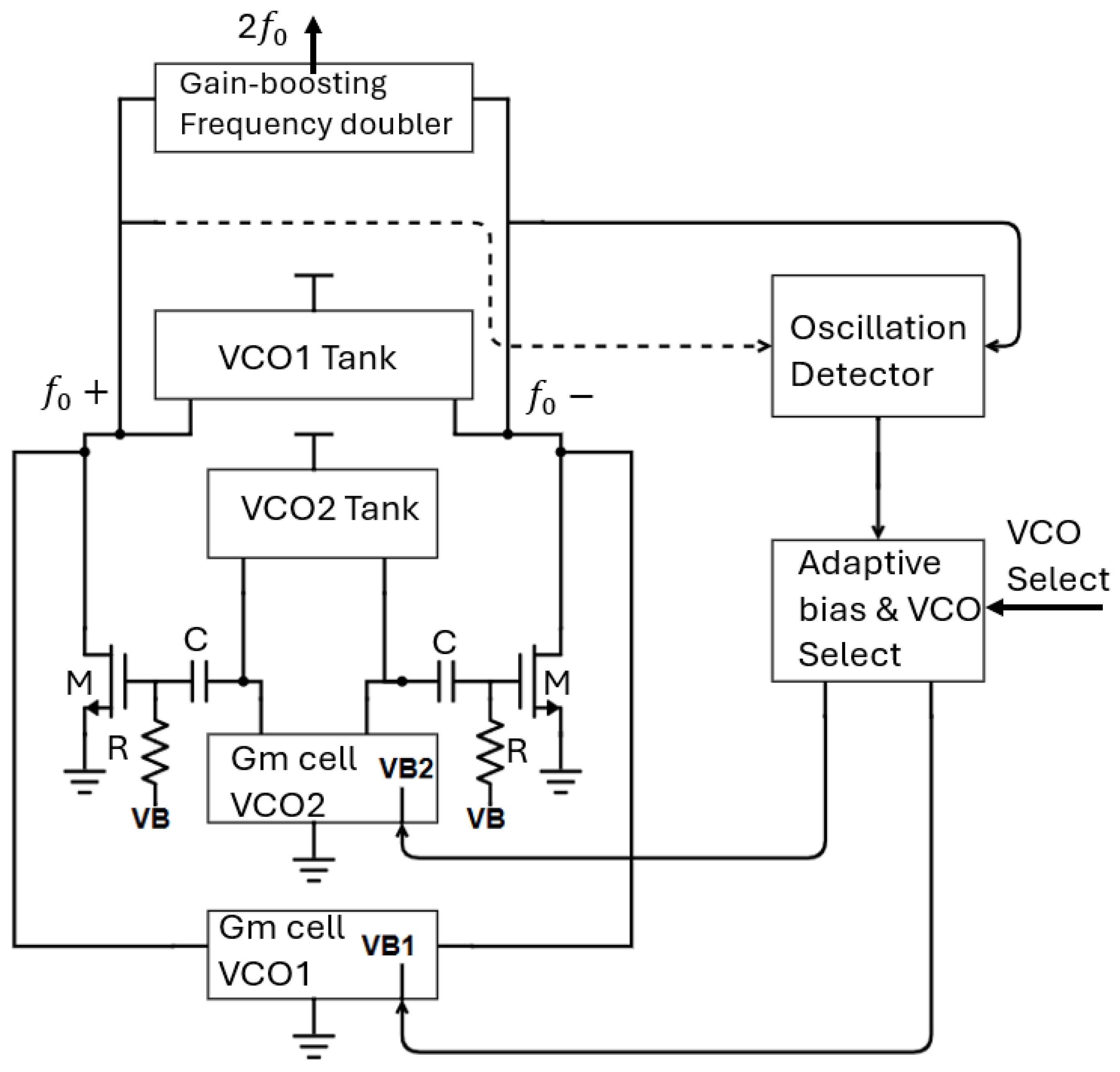
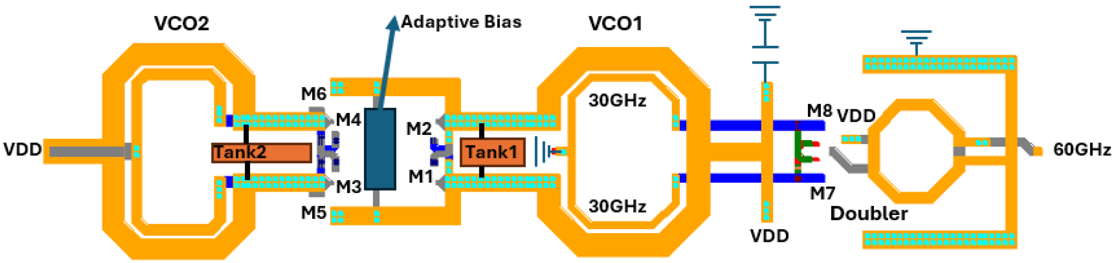
2. Proposed Design
2.1. Proposed Architecture
2.2. Fundamental VCO Considerations
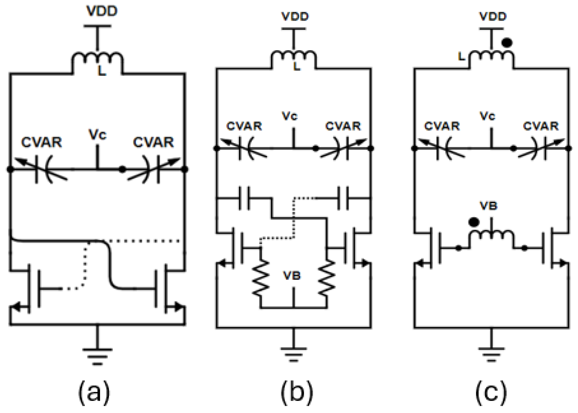
2.2.1. Topology Selection for the Fundamental LO Generation
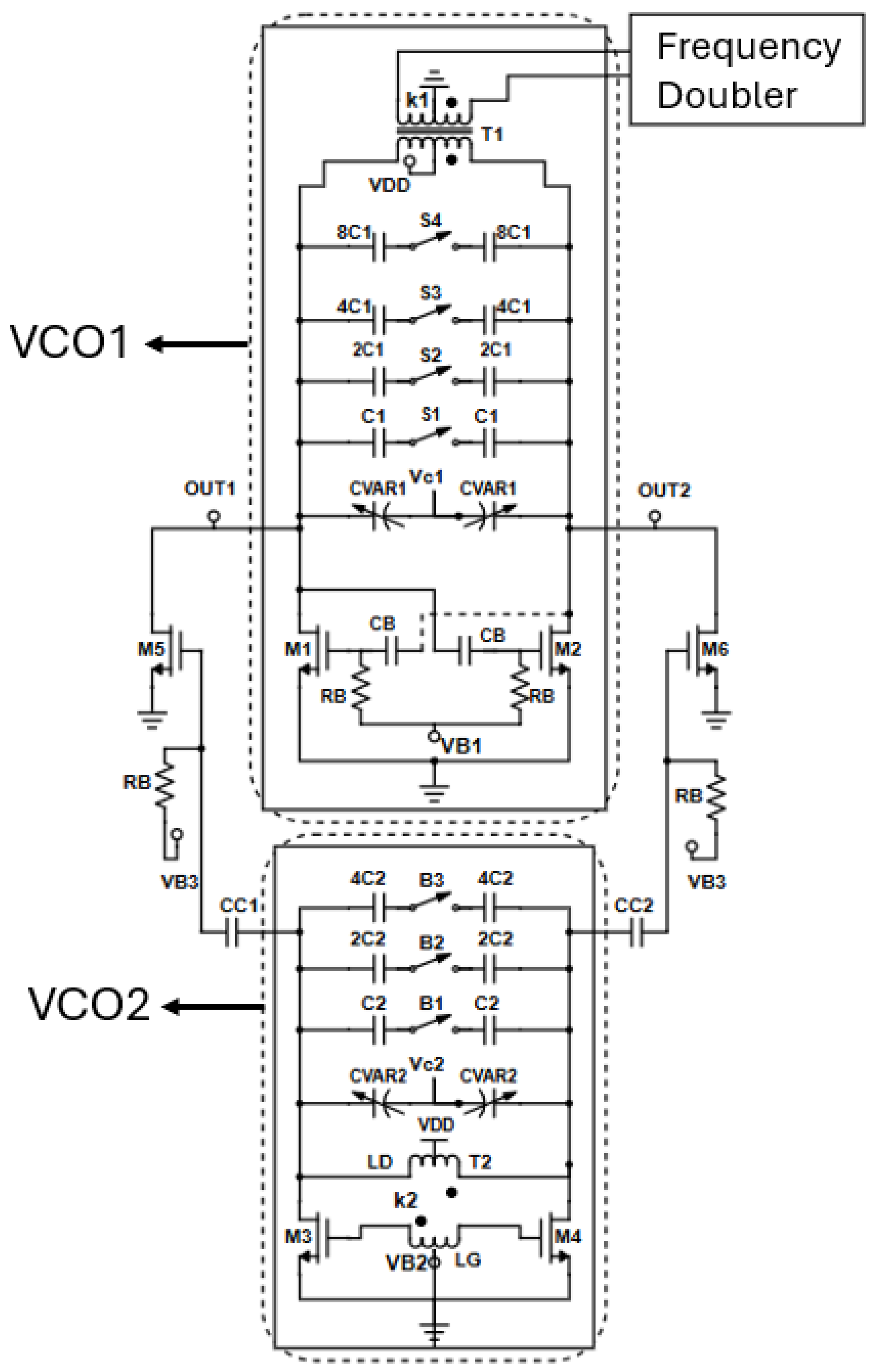
2.2.2. Fundamental Two-Core VCO Design
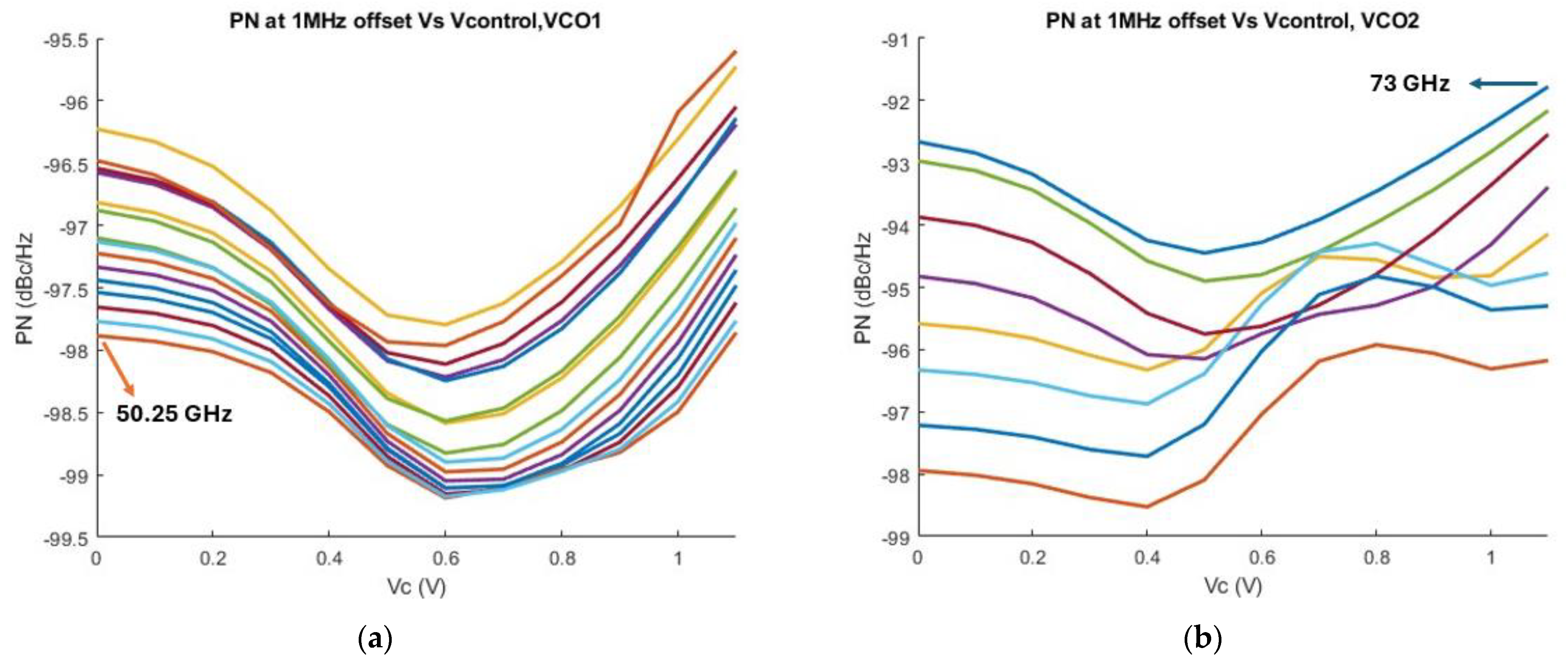
2.2.3. Phase Noise Considerations
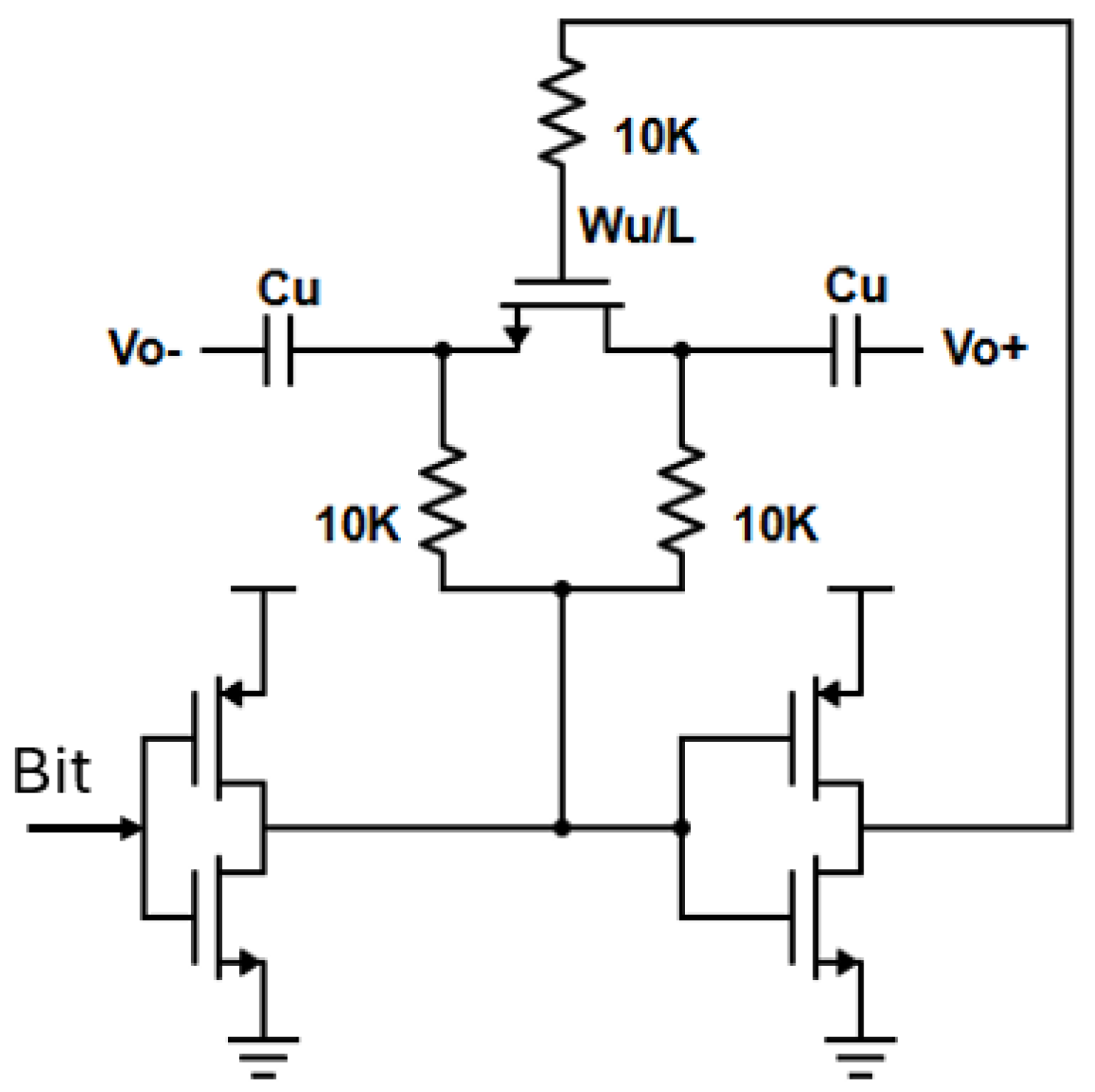
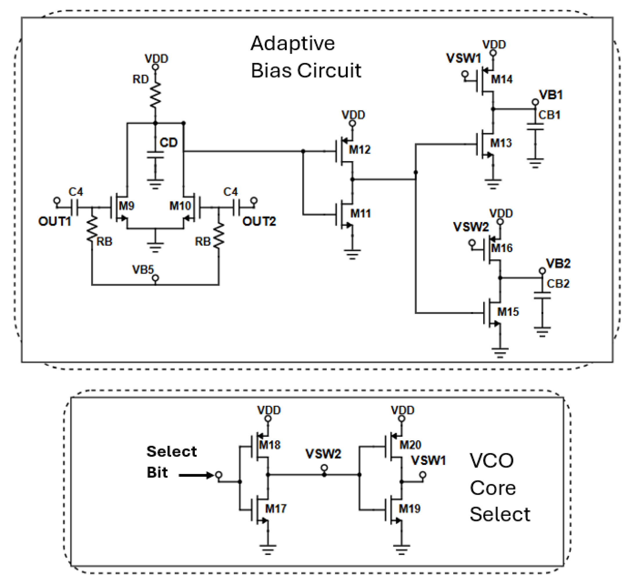
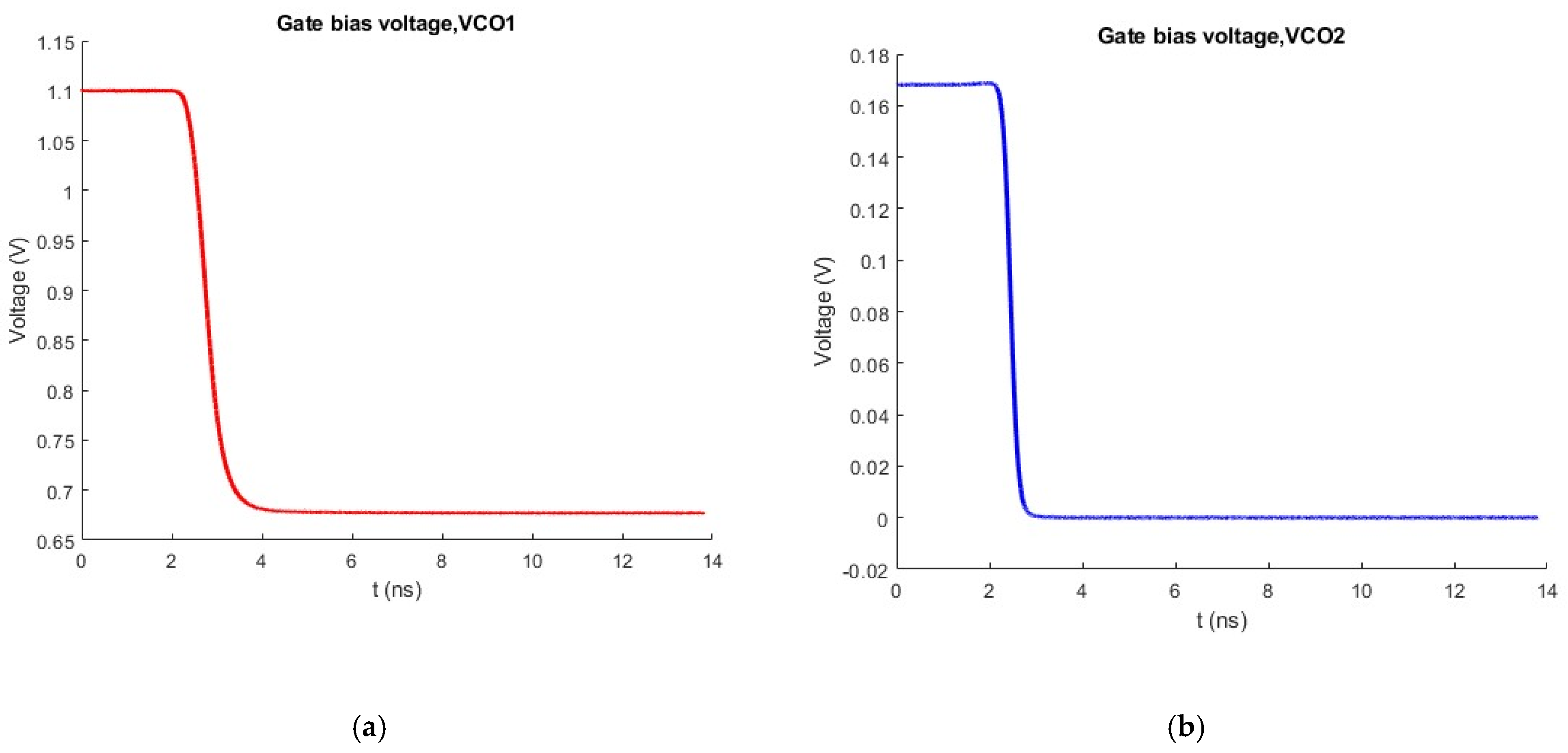
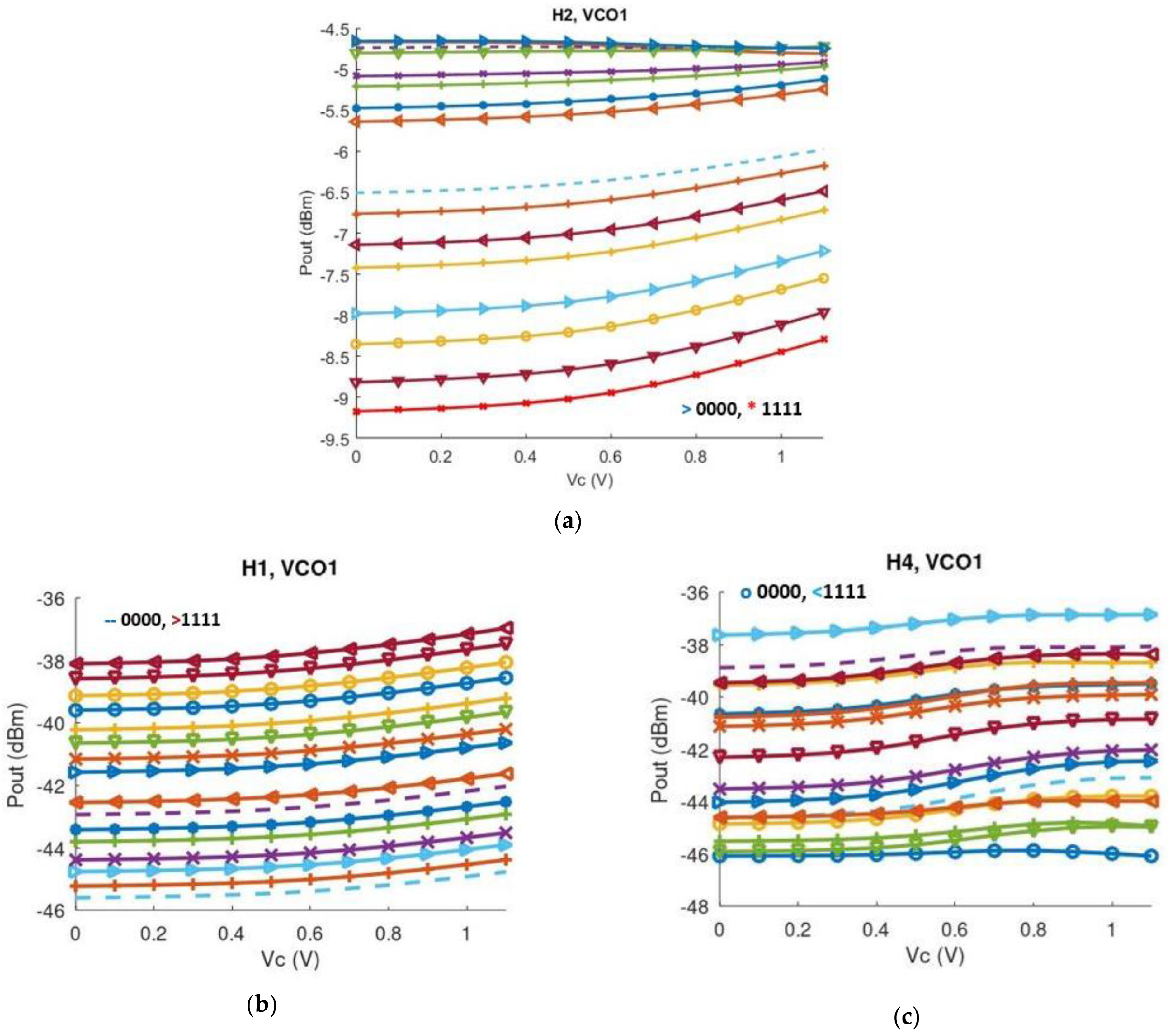
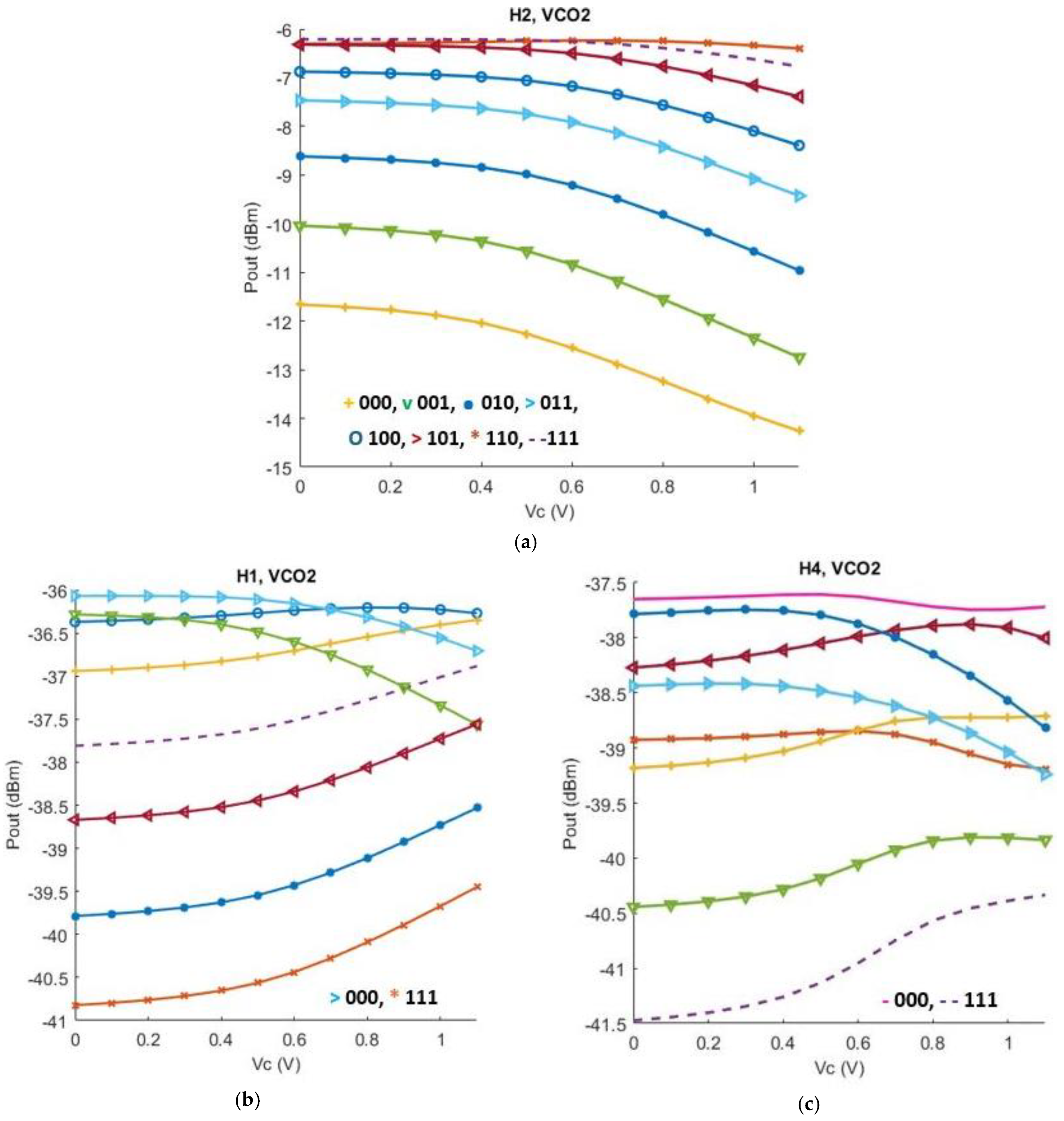
2.2.4. Adaptive Bias and VCO Core Select Circuitry
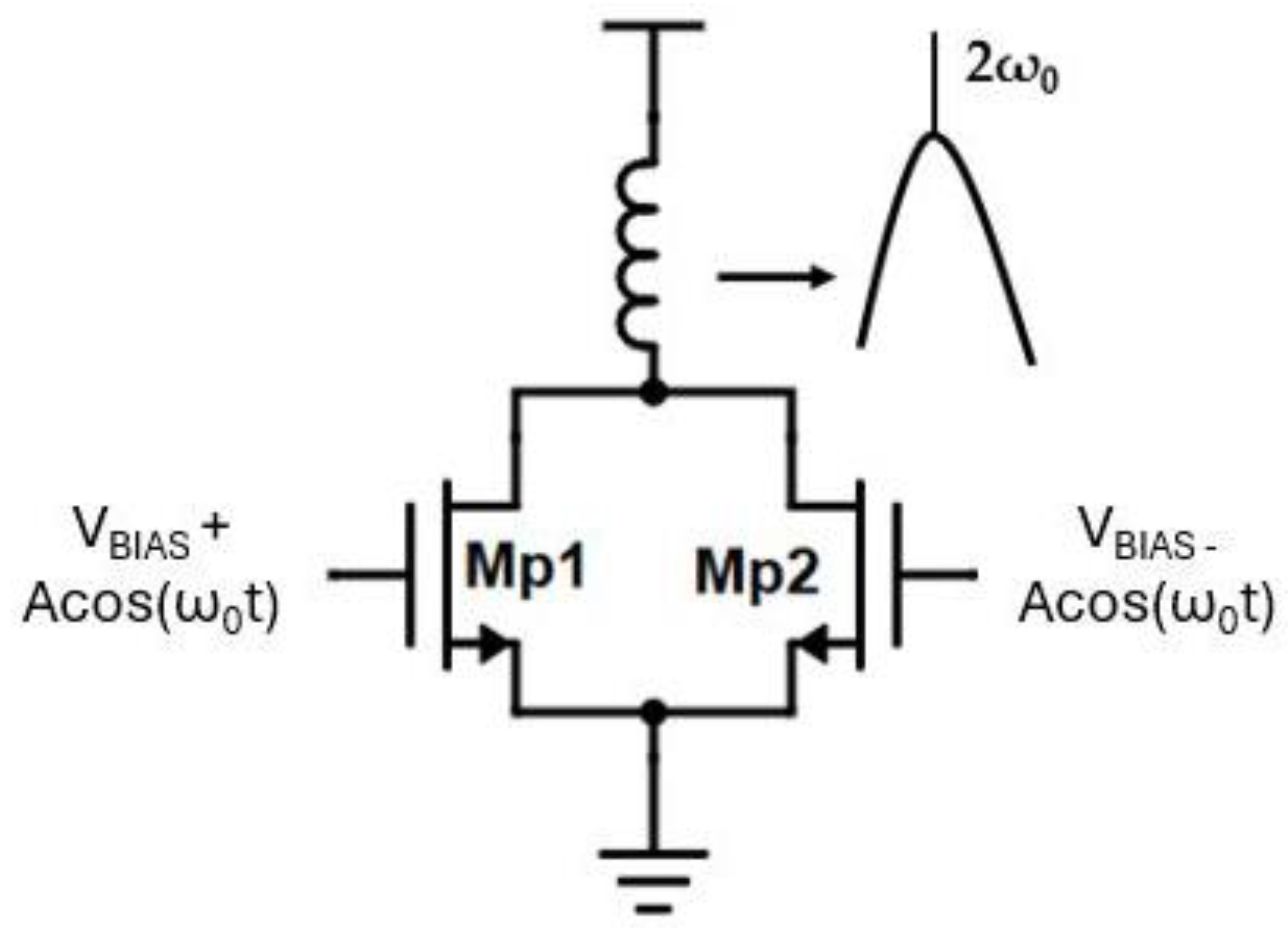
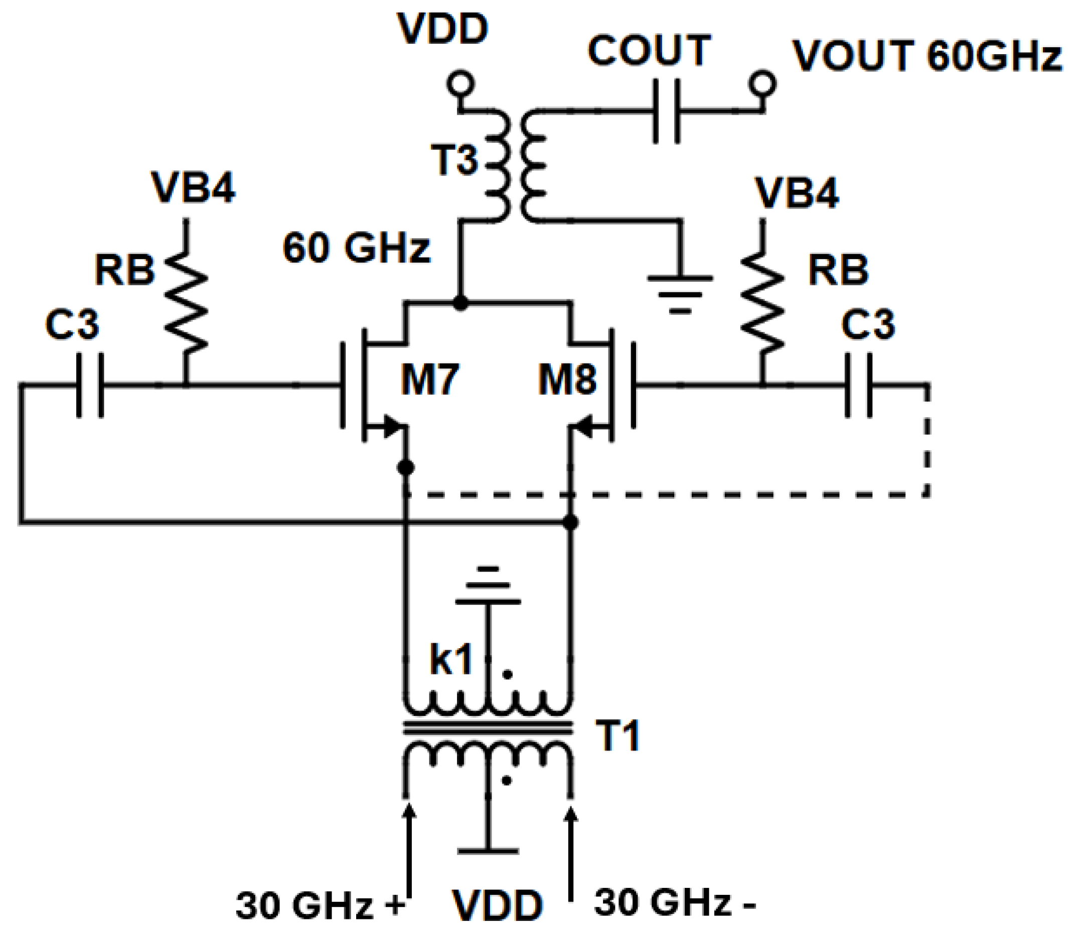
2.3. Gain-Boosted Frequency Doubler
3. Post-Layout Simulation Results
4. Discussion
5. Conclusions
Author Contributions
Funding
Institutional Review Board Statement
Informed Consent Statement
Data Availability Statement
Acknowledgments
Conflicts of Interest
References
- Issakov, V. The State of the Art in CMOS VCOs: Mm-Wave VCOs in Advanced CMOS Technology Nodes. IEEE Microw. Mag. 2019, 20, 59–71. [Google Scholar] [CrossRef]
- Siligaris, A.; Bossuet, A.; Barrau, L.; Antide, E.; Gonzalez-Jimenez, J.; Dehos, C. Fast Chirping 58–64 GHz FMCW Radar Transceiver using D-PROT Multiplier in CMOS 45 nm RFSOI for Vital Signs Detection. In Proceedings of the ESSCIRC 2023—IEEE 49th European Solid State Circuits Conference (ESSCIRC), Lisbon, Portugal, 11–14 September 2023. [Google Scholar] [CrossRef]
- Milosavljević, I.M.; Glavonjić, D.P.; Krčum, D.P.; Jovanović, S.P.; Mihajlović, V.R.; Milovanović, V.M. A 55–64-GHz Fully Integrated Miniaturized FMCW Radar Sensor Module for Short-Range Applications. IEEE Microw. Wirel. Compon. Lett. 2019, 29, 677–679. [Google Scholar] [CrossRef]
- Kankuppe, A.; Park, S.; Renukaswamy, P.T.; Wambacq, P.; Craninckx, J. A Wideband 62-mW 60-GHz FMCW Radar in 28-nm CMOS. IEEE Trans. Microw. Theory Tech. 2021, 69, 2921–2935. [Google Scholar] [CrossRef]
- Xu, C.; Liao, X.; Yang, M.; Hong, F.; Ju, P.; Chen, W. A Packaged 54-to-69-GHz Wideband 2T2R FMCW Radar Transceiver Employing Cascaded-PLL Topology and PTAT-Enhanced Temperature Compensation in 40-nm CMOS. IEEE J. Solid-State Circuits 2024, 59, 3156–3171. [Google Scholar] [CrossRef]
- Oh, K.-I.; Ko, G.-H.; Kim, G.S.; Kim, J.-G.; Baek, D. A 54–64-GHz 4TXs-4RXs CMOS Transceiver with 10-GHz Bandwidth Single Chirp for FMCW Radar Applications. IEEE Trans. Microw. Theory Tech. 2024, 1–13. [Google Scholar] [CrossRef]
- Rimmelspacher, J.; Ciocoveanu, R.; Steffan, G.; Bassi, M.; Issakov, V. Low Power Low Phase Noise 60 GHz Multichannel Transceiver in 28 nm CMOS for Radar Applications. In Proceedings of the 2020 IEEE Radio Frequency Integrated Circuits Symposium (RFIC), Los Angeles, CA, USA, 4–6 August 2020. [Google Scholar] [CrossRef]
- Su, G.; Chen, D.; Pang, K.; Gao, H.; Su, J.; Sun, L. 128.76–129.56 GHz Fundamental Voltage Control Oscillator in 65 nm CMOS. Electronics 2020, 9, 898. [Google Scholar] [CrossRef]
- Stadler, P.; Papurcu, H.; Welling, T.; Tejero Alfageme, S.; Pohl, N. An Overview of State-of-the-Art D-Band Radar System Components. Chips 2022, 1, 121–149. [Google Scholar] [CrossRef]
- Psycharis, I.D.; Tsourtis, V.; Kalivas, G. A 60 GHz low phase noise VCO with second harmonic tail extraction in 40-nm CMOS. AEU-Int. J. Electron. Commun. 2024, 186, 155488. [Google Scholar] [CrossRef]
- Fu, Y.; Li, L.; Wang, D.; Wang, X.; He, L. 28-GHz CMOS VCO with Capacitive Splitting and Transformer Feedback Techniques for 5G Communication IEEE Trans . Very Large Scale Integr. (VLSI) Syst. 2019, 27, 2088–2095. [Google Scholar] [CrossRef]
- Rimmelspacher, J.; Weigel, R.; Issakov, V. Transformer-Coupled Octa-Core 60 GHz Push-Push VCO in a 45-nm RF-SOI CMOS Technology. In Proceedings of the 2019 IEEE International Conference on Microwaves, Antennas, Communications and Electronic Systems (COMCAS), Tel-Aviv, Israel, 4–6 November 2019. [Google Scholar] [CrossRef]
- Shafiullah, Y.; Hietanen, M.; Leinonen, M.E.; Akbar, R.; Aikio, J.; Rusanen, J.; Rahkonen, T.; Pärssinen, A. A Low-Power Push-Push D-Band VCO with 11.6% FTR utilizing Back-gate Control in 22 nm FDSOI. In Proceedings of the 2023 IEEE Radio and Wireless Symposium (RWS), Las Vegas, NV, USA, 22–25 January 2023. [Google Scholar] [CrossRef]
- Peng, Z.; Chen, J.; Wang, H.; Zhang, L.; Hong, W.; Liu, X. A 300 GHz Push-Push Coupling VCO Employing T-Embedded Network in CMOS Technology. IEEE Trans. Terahertz Sci. Technol. 2022, 12, 426–429. [Google Scholar] [CrossRef]
- Nath, S.K.; Yoon, D. A 267 GHz Wide Tuning Range VCO with −3.5 dBm Peak Output Power in 40-nm CMOS. IEEE Trans. Terahertz Sci. Technol. 2023, 13, 122–131. [Google Scholar] [CrossRef]
- Cui, M.; Carta, C.; Ellinger, F. Design of an Ultra Compact Low Power 60 GHz Frequency Doubler in 22 nm FD-SOI. In Proceedings of the 2020 IEEE International Symposium on Radio-Frequency Integration Technology (RFIT), Hiroshima, Japan, 2–4 September 2020. [Google Scholar] [CrossRef]
- Koop-Brinkmann, S.; Steffan, G.; Lasserre, V.; Padovan, F.; Bassi, M.; Issakov, V. A Low Phase Noise VCO for 60 GHz Radar Applications with a Direct Transformer-Based Fourth Harmonic Extraction in 28 nm CMOS. In Proceedings of the 2024 19th European Microwave Integrated Circuits Conference (EuMIC), Paris, France, 23–24 September 2024. [Google Scholar] [CrossRef]
- Gupta, A.; Dietz, M.; Engelmann, A.; Hagelauer, A. Ultra-Low Power 60 GHz Class-C Frequency Tripler in 22-nm FDSOI CMOS Technology. In Proceedings of the 2024 IEEE 15th Latin America Symposium on Circuits and Systems (LASCAS), Punta del Este, Uruguay, 27 February–1 March 2024. [Google Scholar] [CrossRef]
- Hueber, G.; Niknejad, A.M. Millimeter-Wave Circuits for 5G and Radar, 2nd ed.; Cambridge University Press: Cambridge, UK, 2019. [Google Scholar] [CrossRef]
- Cui, M.; Carta, C.; Elinger, F. Two 60-GHz 15-dBm Output Power VCOs in 22-nm FDSOI. IEEE Microw. Wirel. Compon. Lett. 2021, 31, 184–187. [Google Scholar] [CrossRef]
- Wang, X.; Li, L.; Wang, D.; Fu, Y. 60 GHz CMOS VCO with Transformer Feedback Techniques. In Proceedings of the 2020 IEEE MTT-S International Wireless Symposium (IWS), Shanghai, China, 20–23 September 2020. [Google Scholar] [CrossRef]
- Balamurali, S.; Mangraviti, G.; Tsai, C.-H.; Wambacq, P.; Craninckx, J. Design and Analysis of 55–63-GHz Fundamental Quad-Core VCO with NMOS-Only Stacked Oscillator in 28-nm CMOS. IEEE J. Solid-State Circuits 2022, 57, 1997–2010. [Google Scholar] [CrossRef]
- Barajas, B.; Molavi, R.; Mirabbasi, S. A Wideband 65-nm 60-GHz Push-Push LC VCO using a Nonlinear Varactor Array. In Proceedings of the 2024 IEEE 67th International Midwest Symposium on Circuits and Systems (MWSCAS), Springfield, MA, USA, 11–14 August 2024. [Google Scholar] [CrossRef]
- Rimmelspacher, J.; Weigel, R.; Hagelauer, A.; Issakov, V. A Quad-Core 60 GHz Push-Push 45 nm SOI CMOS VCO with −101.7 dBc/Hz Phase Noise at 1 MHz offset, 19% Continuous FTR and −187 dBc/Hz FoMT. In Proceedings of the ESSCIRC 2018—IEEE 44th European Solid State Circuits Conference (ESSCIRC), Dresden, Germany, 3–6 September 2018. [Google Scholar] [CrossRef]
- Psycharis, I.D.; Tsourtis, V.; Kalivas, G. A 30 GHz Class-C Switchless Dual-Band Two Core VCO in 40-nm CMOS. In Proceedings of the 2024 13th International Conference on Modern Circuits and Systems Technologies (MOCAST), Sofia, Bulgaria, 26–28 June 2024. [Google Scholar] [CrossRef]
- Hejazi, A.; Pu, Y.; Lee, K.-Y. A Design of Wide-Range and Low Phase Noise Linear Transconductance VCO with 193.76 dBc/Hz FoMT for mm-Wave 5G Transceivers. Electronics 2020, 9, 935. [Google Scholar] [CrossRef]
- Nguyen, T.N.; Lee, J.-W. Ultralow-Power Ku-Band Dual-Feedback Armstrong VCO with a Wide Tuning Range. IEEE Trans. Circuits Syst. II Express Briefs 2012, 59, 394–398. [Google Scholar] [CrossRef]
- Esmaeeli, O.; Lightbody, S.; Masnadi Shirazi, A.H.; Djahanshahi, H.; Zavari, R.; Mirabbasi, S.; Shekhar, S. A Transformer-Based Technique to Improve Tuning Range and Phase Noise of a 20–28GHz LCVCO and a 51–62GHz Self-Mixing LCVCO. IEEE Trans. Circuits Syst. I Regul. Pap. 2022, 69, 2351–2363. [Google Scholar] [CrossRef]
- Lee, J.-Y.; Kim, G.S.; Ko, G.-H.; Oh, K.-I.; Park, J.G.; Baek, D. Low Phase Noise and Wide-Range Class-C VCO Using Auto-Adaptive Bias Technique. Electronics 2020, 9, 1290. [Google Scholar] [CrossRef]
- Kim, J.; Mauludin, M.F.; Azzahra, H.A.; Jhon, H.; Lee, S.; Cho, K. An 18–19.2 GHz Voltage-Controlled Oscillator with a Compact Varactor-Only Capacitor Array. Electronics 2023, 12, 1532. [Google Scholar] [CrossRef]
- Razavi, B. RF Microelectronics, 2nd ed.; Prentice Hall Press: Upper Saddle River, NJ, USA, 2011. [Google Scholar]
- Fanori, L.; Andreani, P. Highly Efficient Class-C CMOS VCOs, Including a Comparison with Class-B VCOs. IEEE J. Solid-State Circuits 2013, 48, 1730–1740. [Google Scholar] [CrossRef]
- Wu, X.; Kang, Z.; Wang, Y.; Wu, L. A 53–78 GHz Complementary Push–Push Frequency Doubler with Implicit Dual Resonance for Output Power Combining. IEEE Trans. Circuits Syst. I Regul. Pap. 2023, 70, 1202–1213. [Google Scholar] [CrossRef]
- Yang, C.-Y.; Chang, C.-H.; Lin, J.-M.; Chang, H.-Y. A 20/40-GHz Dual-Band Voltage-Controlled Frequency Source in 0.13-μm CMOS. IEEE Trans. Microw. Theory Tech. 2011, 59, 2008–2016. [Google Scholar] [CrossRef]
- So, C.; Hong, S. A V-Band Differential Push–Push Frequency Doubler with a Current-Reuse gm-Boosted Buffer. IEEE Microw. Wirel. Technol. Lett. 2023, 33, 299–302. [Google Scholar] [CrossRef]
- He, H.; Yang, H.; Huang, J.; Zhang, J.; Yan, X.; Guo, Y. A 59–65 GHz Frequency Generator Based on 20 GHz VCO and Tripler with Low Phase Noise and Low Power Consumption in 40-nm CMOS. In Proceedings of the 2023 IEEE MTT-S International Wireless Symposium (IWS), Qingdao, China, 14–17 May 2023. [Google Scholar] [CrossRef]
- Issakov, V.; Padovan, F.; Rimmelspacher, J.; Weige, R.; Geiselbrechtinger, A. A 52-to-61 GHz Push-Push VCO in 28 nm CMOS. In Proceedings of the 2018 48th European Microwave Conference (EuMC), Madrid, Spain, 23–27 September 2018. [Google Scholar] [CrossRef]


| Parameter | Value |
|---|---|
| WM1-M4 | 18 × 1 μm |
| WM5-M6 | 22 × 1 μm |
| L | 40 nm |
| CB | 82 fF |
| RB | 4 K |
| VB3 | 570 mV |
| CCC1 | 42 fF |
| LC Tanks Parameters | Values |
|---|---|
| C1, C2 | 15.3 fF, 24.7 fF |
| WSwitch,S1, WSwitch,B1 | 12 × 1 μm, 24 × 1 μm |
| LSwitch,S1–S4, LSwitch,B1–B3 | 40 nm |
| CVAR1, CVAR2@VGS = 0 | 30 fF, 36 fF |
| T1: LP1, LP2, QP1, QP2 | 245 pH, 247 pH, 24, 13.7 |
| T2: LD, LG, QD, QG | 240 pH, 265 pH, 22.1, 13.4 |
| Parameter | Value | Parameter | Value |
|---|---|---|---|
| C4 | 42.5 fF | WM12, WM18, M20 | 32 × 5 μm, 10 × 3 μm |
| WM9,M10,WM13,M15 | 12 × 1 μm, 22 × 2 μm | WM14, M16 | 30 × 5 μm |
| WM11,M17,M19 | 10 × 1 μm | LM13-M16 | 90 nm |
| RD, RB | 4.6 K, 6 K | CB1-B2, CD | 4 pF, 3 pF |
| Parameter | Value |
|---|---|
| WM7, M8 | 8 × 1 μm |
| LM7, M8 | 40 nm |
| VB4 | 0.4 V |
| C3 | 75 fF |
| RB | 3 K |
| Cout | 35 fF |
| T3:LP/QP at 60 GHz | 210 pH/17 |
| T3:LP/QP at 60 GHz | 196 pH/14 |
| Corners | Frequency (GHz) | PN 1 MHz | PN 1 MHz | Pout dBm. | Pout dBm. |
|---|---|---|---|---|---|
| TT | 50.25–73 | −97.9 | −92.1 | −9.2 | −14.2 |
| SS | 47.5–71.2 | −96.5 | −91.3 | −15.3 | −17.2 |
| FF | 53.7–75.3 | −97.8 | −93 | −8.2 | −13.5 |
| TT @ 120 °C | 49.5–72.8 | −94.8 | −90.2 | −12 | −16.9 |
| TT @ −40 °C | 50.9–73.3 | −98 | −92.8 | −7.9 | −12.9 |
| Reference | Hardware | FREQ (GHz) | PN [dBc/Hz] @ 1 MHz | PDC,VCO (mW) | FTR (%) | Pout (dBm) | ) | FOM * | * | Process |
|---|---|---|---|---|---|---|---|---|---|---|
| [17] | measured | 60.85 | −99.8 | 11.7 | 15.6 | - | 0.12 1 | −184.1 | −188 | 28 nm CMOS |
| [21] | measured | 61.3 | −94.9 | 8.4 | 9 | −10 | 0.009 1 | −183.4 | −180.5 | 65 nm CMOS |
| [22] | measured | 59 | −95 | 15.3 | 13.4 | −4 | 0.12 1 | −178 | −180.5 | 28 nm CMOS |
| [23] | Post- layout | 60 | −93.5 | 4.2 | 18.2 | −12 | 0.07 1 | −183 | −188 | 65 nm CMOS |
| [24] | measured | 61.4 | −96.9 | 20 | 18 | −22.6 | 0.08 1 | −180 | −186 | 45 nm SOI |
| [28] | measured | 58.9 | −92.5 | 4.7 | 18.5 | - | 0.17 1 | −181.7 | −187.1 | 65 nm CMOS |
| [36] | Post- layout | 62.4 | −97.2 | 16 | 10.58 | - | 0.052 1 | −181.2 | −181.5 | 40 nm CMOS |
| [37] | measured | 60 | −87 | 11 | 16 | −23 | 0.02 | −173 | −177 | 28 nm CMOS |
| This work | Post- layout | 61.6 | −96.7 | 11.3 2 | 36.92 | −8.4 | 0.1 1 | −181.7 | −192.6 | 40 nm CMOS |
Disclaimer/Publisher’s Note: The statements, opinions and data contained in all publications are solely those of the individual author(s) and contributor(s) and not of MDPI and/or the editor(s). MDPI and/or the editor(s) disclaim responsibility for any injury to people or property resulting from any ideas, methods, instructions or products referred to in the content. |
© 2025 by the authors. Licensee MDPI, Basel, Switzerland. This article is an open access article distributed under the terms and conditions of the Creative Commons Attribution (CC BY) license (https://creativecommons.org/licenses/by/4.0/).
Share and Cite
Psycharis, I.D.; Tsourtis, V.; Kalivas, G. A 60 GHz Class-C Wide Tuning-Range Two-Core VCO Utilizing a Gain-Boosting Frequency Doubling Technique and an Adaptive Bias Scheme for Robust Startup. Sensors 2025, 25, 981. https://doi.org/10.3390/s25030981
Psycharis ID, Tsourtis V, Kalivas G. A 60 GHz Class-C Wide Tuning-Range Two-Core VCO Utilizing a Gain-Boosting Frequency Doubling Technique and an Adaptive Bias Scheme for Robust Startup. Sensors. 2025; 25(3):981. https://doi.org/10.3390/s25030981
Chicago/Turabian StylePsycharis, Ioannis Dimitrios, Vasileios Tsourtis, and Grigorios Kalivas. 2025. "A 60 GHz Class-C Wide Tuning-Range Two-Core VCO Utilizing a Gain-Boosting Frequency Doubling Technique and an Adaptive Bias Scheme for Robust Startup" Sensors 25, no. 3: 981. https://doi.org/10.3390/s25030981
APA StylePsycharis, I. D., Tsourtis, V., & Kalivas, G. (2025). A 60 GHz Class-C Wide Tuning-Range Two-Core VCO Utilizing a Gain-Boosting Frequency Doubling Technique and an Adaptive Bias Scheme for Robust Startup. Sensors, 25(3), 981. https://doi.org/10.3390/s25030981