

A Low-Power Complementary Metal-Oxide-Semiconductor Receiver with Quadrature Bandpass Continuous-Time Delta–Sigma Analog-to-Digital Converter for IoT Applications

Abstract
:1. Introduction
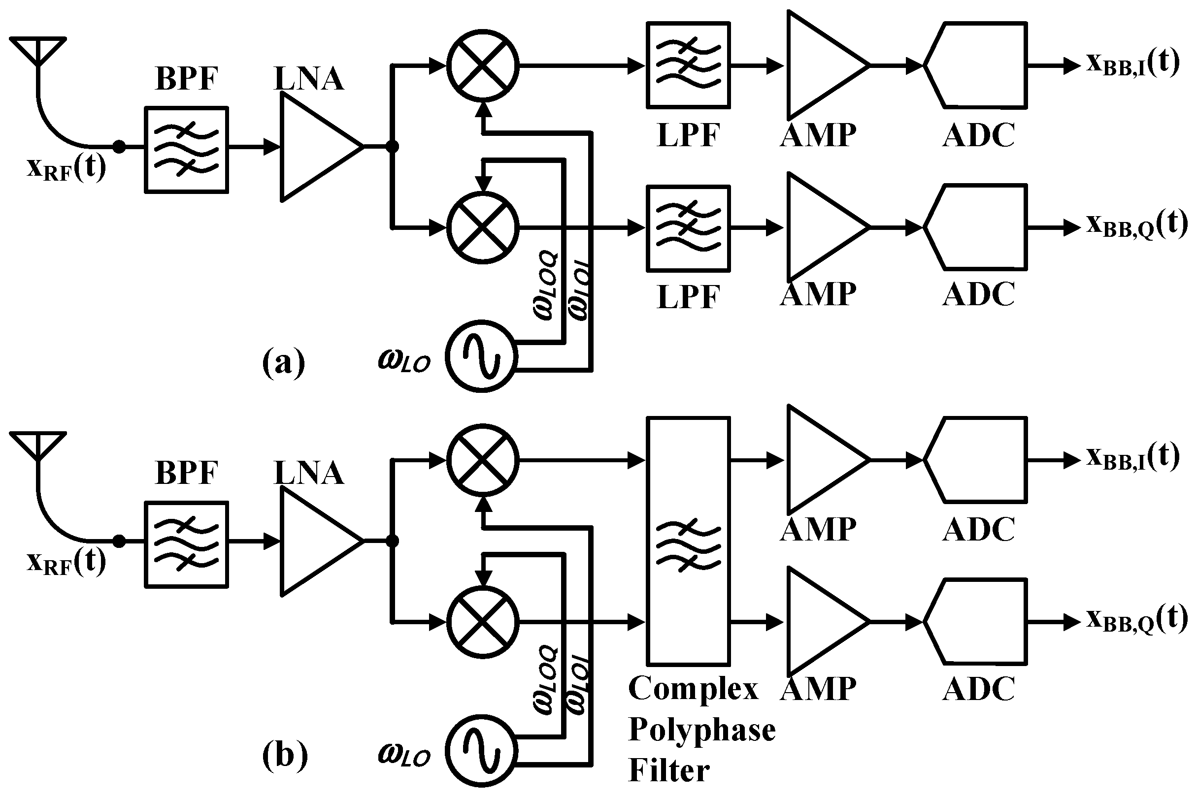
2. A Comparative Analysis of IoT Receiver Architectures
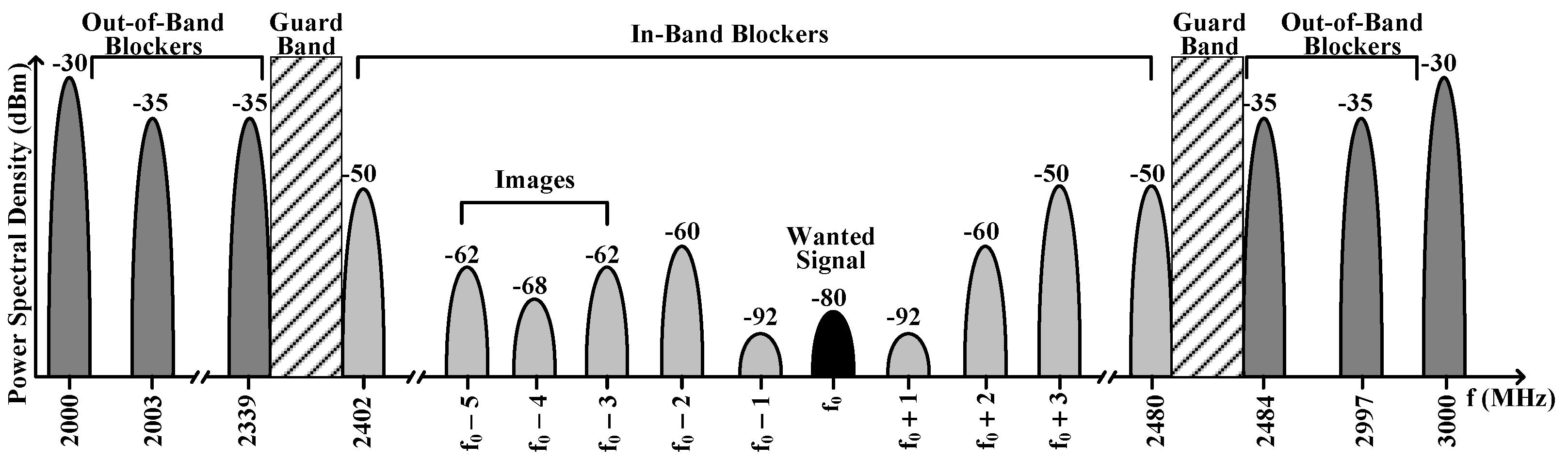
3. Optimizing ADC Dynamic Range for BLE Protocol: A Comprehensive Analysis
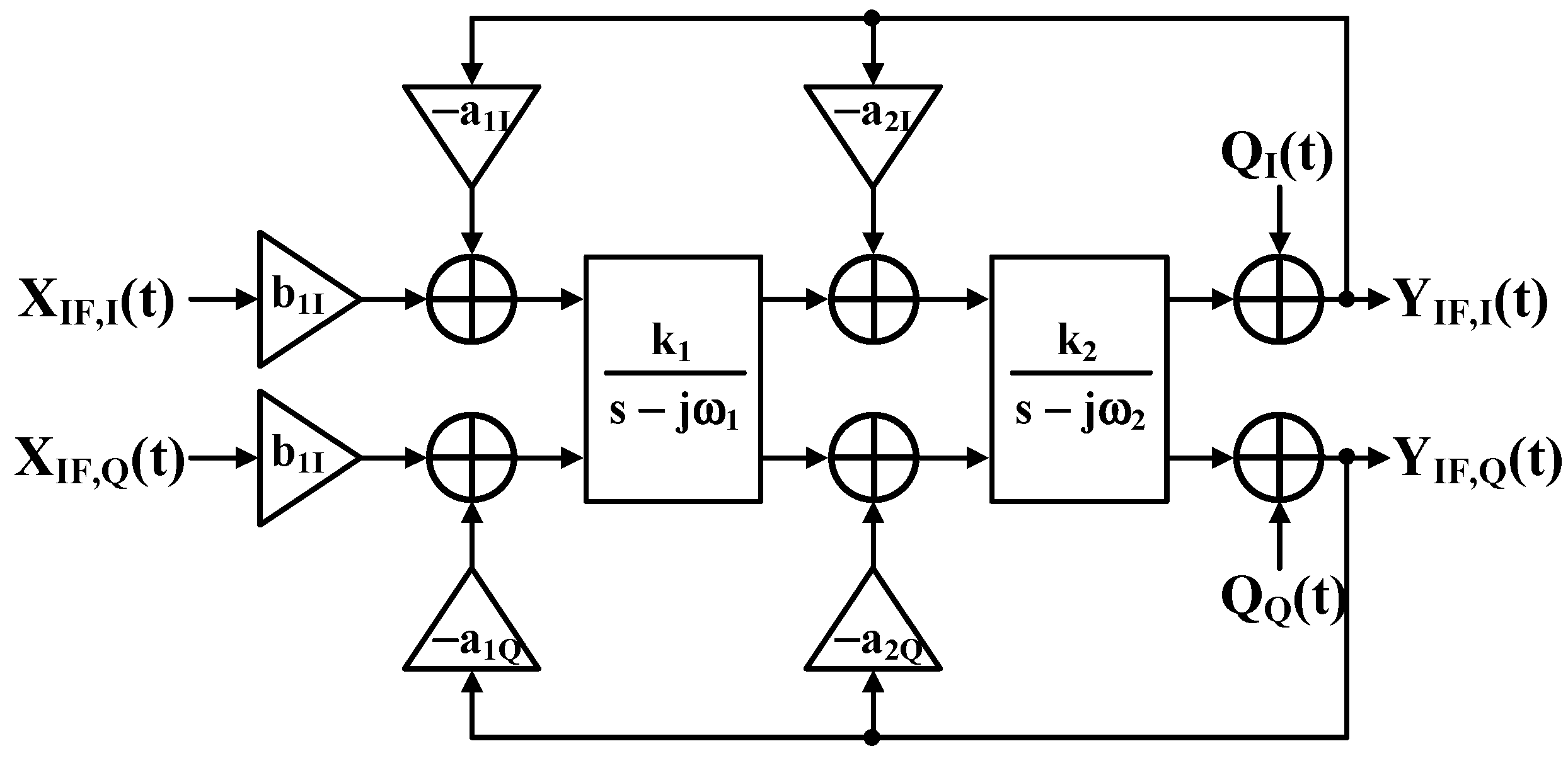
4. Complex Continuous-Time Delta–Sigma ADCs: Principles and Challenges
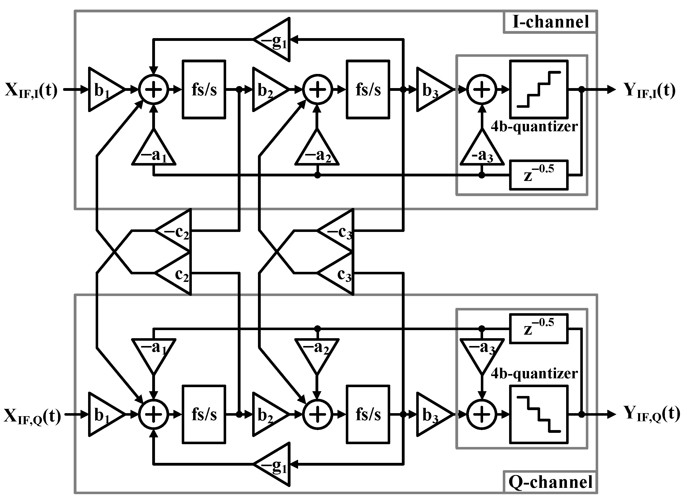
5. Proposed Quadrature Bandpass Continuous-Time Delta–Sigma ADC
5.1. Quadrature Bandpass Continuous-Time Delta–Sigma ADC Architecture
5.2. Quadrature Bandpass Continuous-Time Delta–Sigma ADC Circuit Design
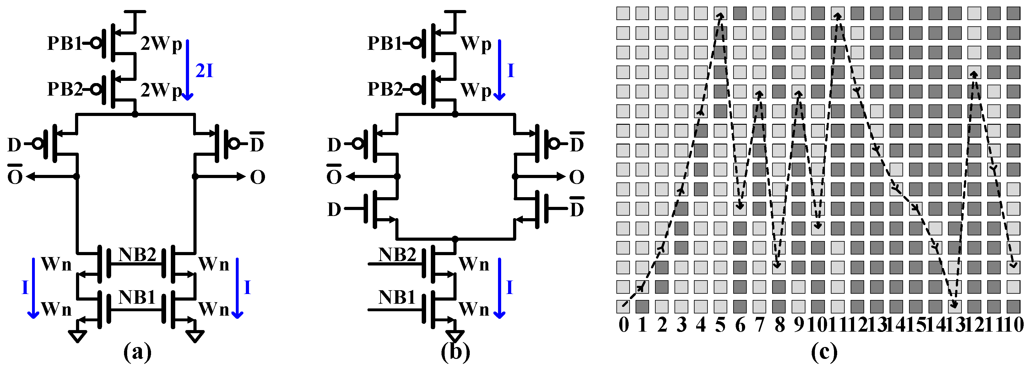
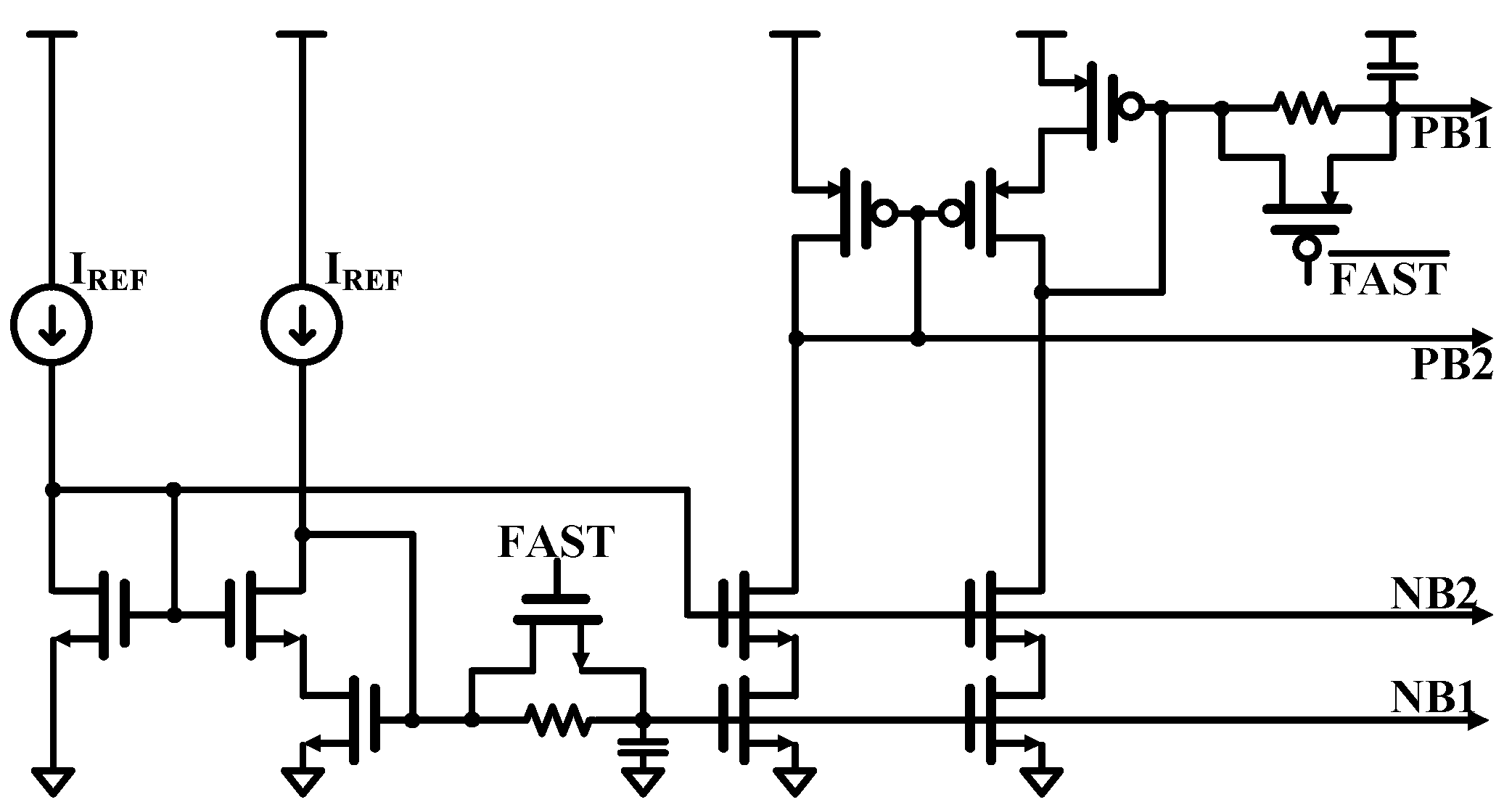
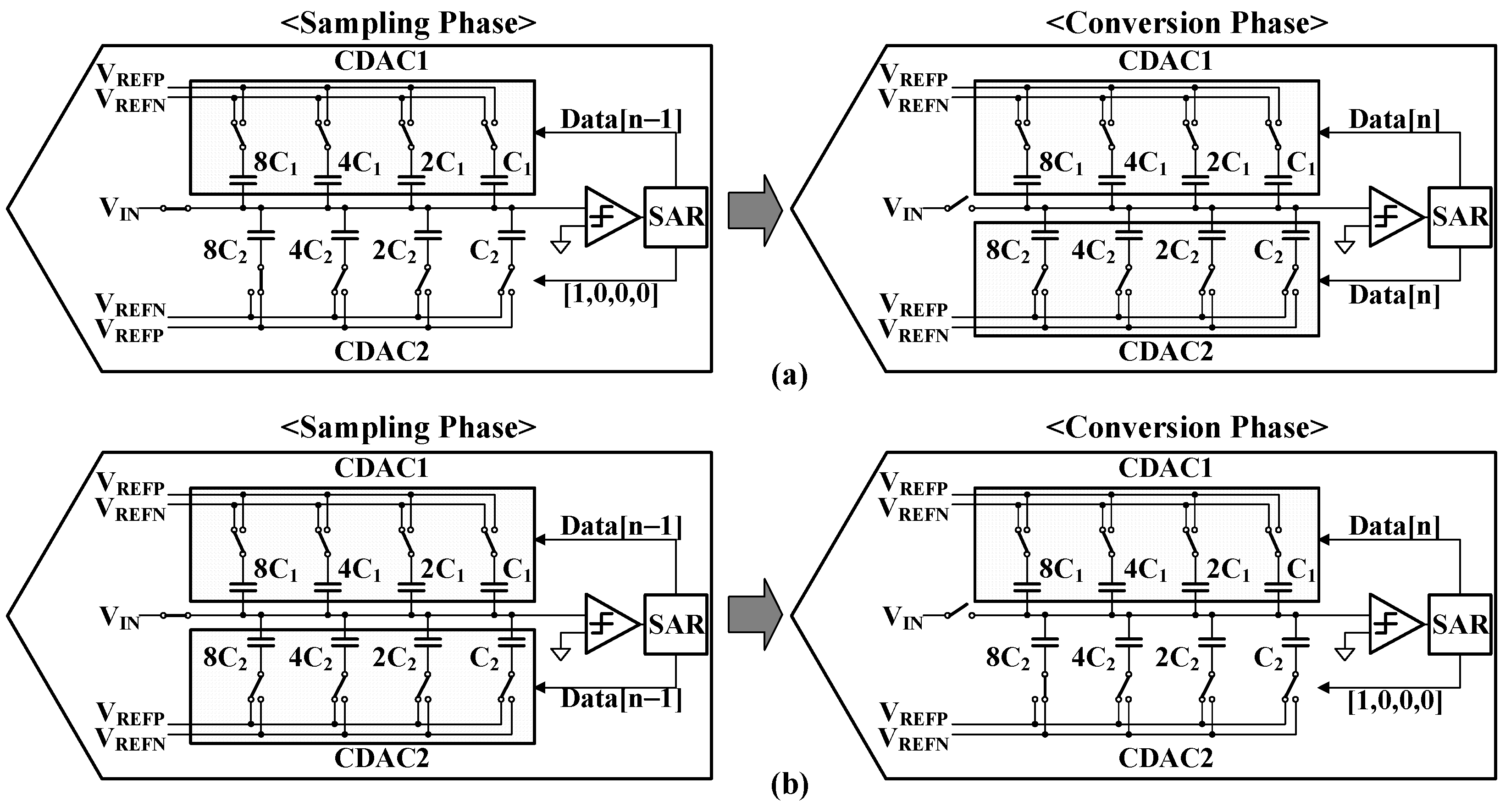
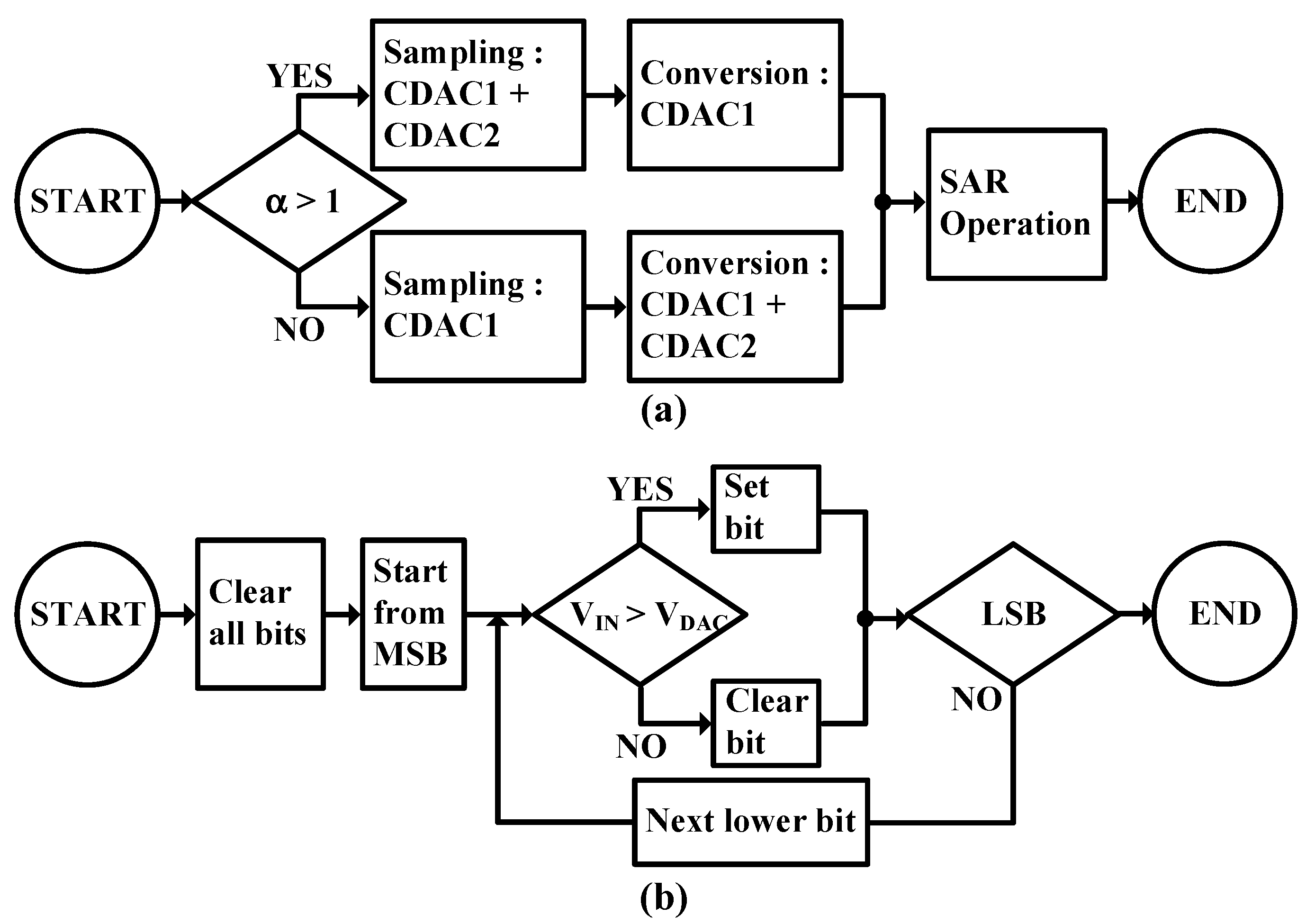
5.2.1. Four-Bit Feedback Current Digital-to-Analog Converter Circuit
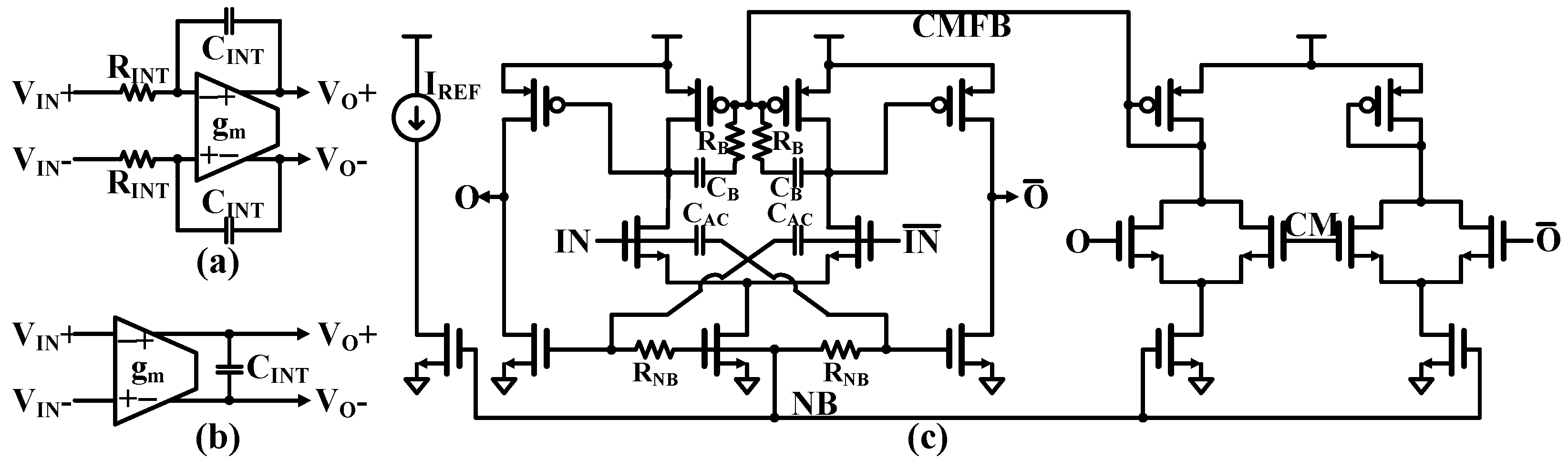
5.2.2. Active-RC Integrator with Proposed OTA
5.2.3. Four-Bit Quantizer
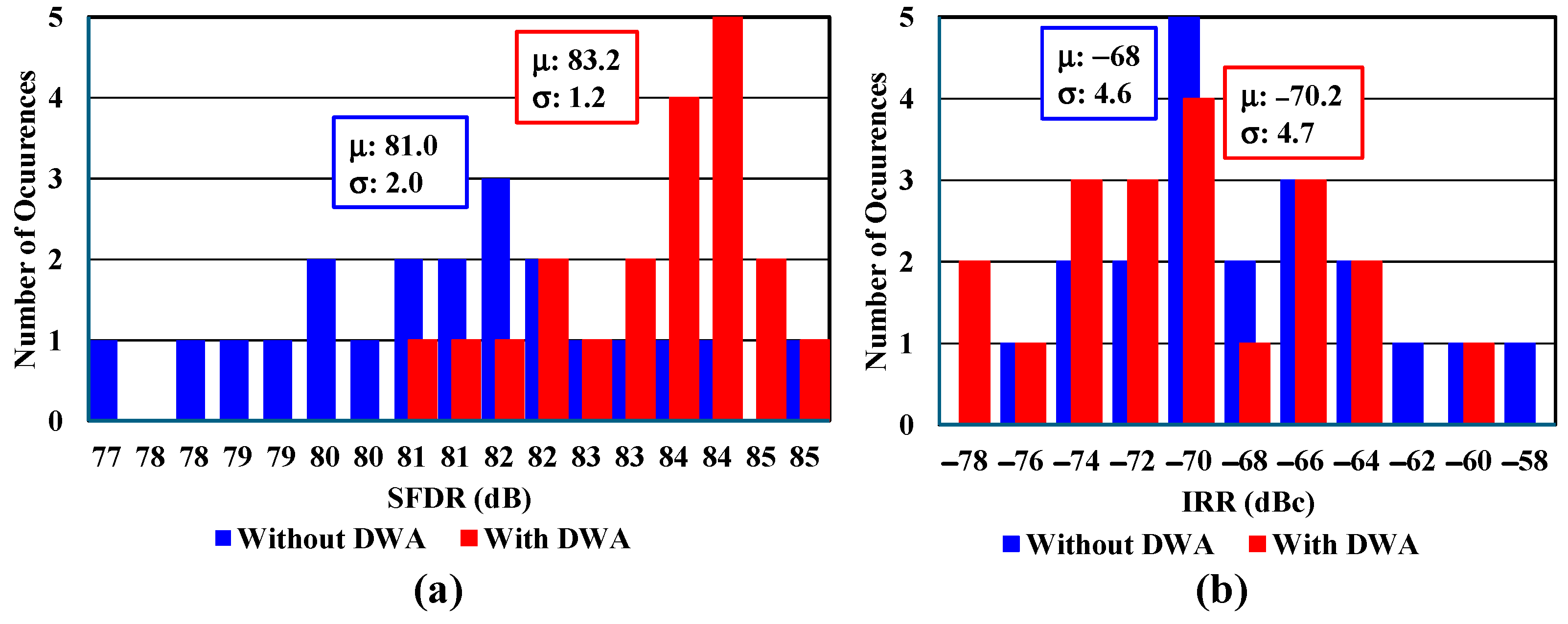
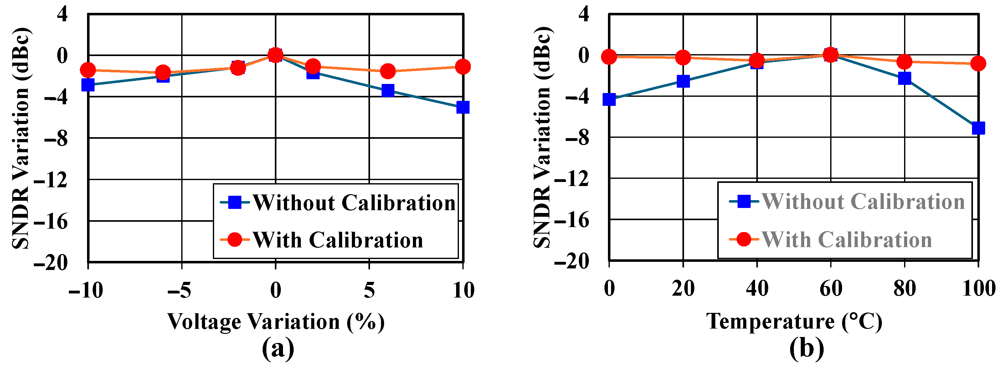
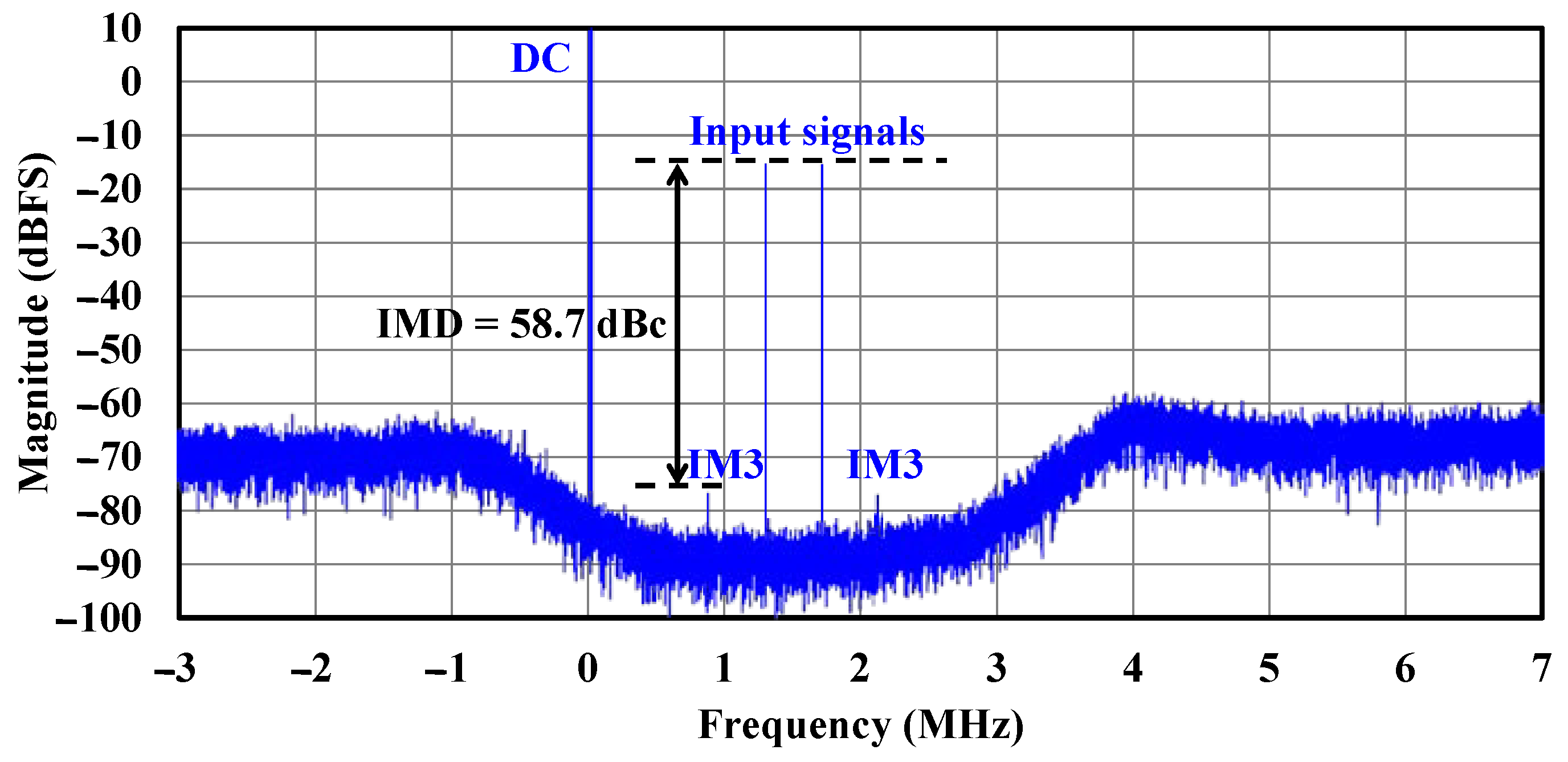
6. Experimental Results
7. Conclusions
Funding
Institutional Review Board Statement
Informed Consent Statement
Data Availability Statement
Conflicts of Interest
References
- Zhang, Y.; Zhang, F.; Shakhsheer, Y.; Silver, J.D.; Klinefelter, A.; Nagaraju, M.; Boley, J.; Pandey, J.; Shrivastava, A.; Carlson, E.J.; et al. A Batteryless 19 μW MICS/ISM-Band Energy Harvesting Body Sensor Node SoC for ExG Applications. IEEE J. Solid-State Circuits 2013, 48, 199–213. [Google Scholar] [CrossRef]
- Cavliwireless. Communication Protocols in IoT. Available online: https://www.cavliwireless.com/blog/nerdiest-of-things/communication-protocols-in-iot.html (accessed on 28 December 2024).
- Dusuniot. Zigbee vs. BLE vs. Bluetooth Mesh, Choosing the Best or Combining Them. Available online: https://www.dusuniot.com/blog/zigbee-vs-bluetooth-le-and-mesh/ (accessed on 28 December 2024).
- Pavan, S.; Schreier, R.; Temes, G.C. Understanding Delta-Sigma Data Converters, 2nd ed.; Wiley-IEEE Press: Hoboken, NJ, USA, 2017. [Google Scholar]
- Chen, H.; Wang, L.; Li, T.; He, L.; Lin, F. A 0.6 V 19.5 μW 80 dB DR ΔΣ Modulator with SA-Quantizers and Digital Feedforward Path. J. Circuits Syst. Comput. 2017, 26, 1750117. [Google Scholar] [CrossRef]
- Zhang, Y.; Zhang, C.; Zhang, Y. Design Strategies and Architectures for Ultra-Low-Voltage Delta-Sigma ADCs. Electronics 2021, 10, 1156. [Google Scholar] [CrossRef]
- Gao, W. Energy and Bandwidth-Efficient Wireless Transmission; Springer: Singapore, 2017. [Google Scholar]
- Prabhala, V.A.; Baddipadiga, B.P.; Fajri, P.; Ferdowsi, M. An Overview of Direct Current Distribution System Architectures & Benefits. Energies 2018, 11, 2463. [Google Scholar] [CrossRef]
- Jin, Y.; Wu, Y.; Xiao, Z.; Huang, F.; Yu, Y. A 400-μW IoT Low-IF Voltage-Mode Receiver Front-End with Charge-Sharing Complex Filter. IEEE Trans. Circuits Syst. I Regul. Pap. 2022, 69, 3279–3292. [Google Scholar] [CrossRef]
- Regulagadda, S.S.; Naseeb, A.; Samad, S.A.; Manoharan, S. A 1.5 mA, 2.4 GHz ZigBee/BLE QLMVF Receiver Frond End with Split TCAs in 180 nm CMOS. In Proceedings of the 2016 29th International Conference on VLSI Design and 2016 15th International Conference on Embedded Systems (VLSID), Kolkata, India, 4–8 January 2016; pp. 207–212. [Google Scholar] [CrossRef]
- Xiang-Ning, F.; Yu-Tao, S. An Efficient CMOS DC Offset Cancellation Circuit for PGA of Low IF Wireless Receivers. In Proceedings of the 2010 International Conference on Microwave and Millimeter Wave Technology, Chengdu, China, 8–11 May 2010; pp. 1449–1452. [Google Scholar] [CrossRef]
- Hwang, I.-S.; Yoo, S.-S.; Song, S.-H.; Park, J.-K.; Choi, S.-I.; Choi, J.-J. A Folded RF Front-end with Low Flicker Noise for Bluetooth and ZigBee application. In Proceedings of the 2007 IEEE International Symposium on Circuits and Systems, New Orleans, LA, USA, 27–30 May 2007; pp. 781–784. [Google Scholar] [CrossRef]
- Almradi, A.; Hamdi, K.A. IQI Mitigation for Narrowband IoT Systems with OFDM-IM. IEEE Access 2018, 6, 44989–45000. [Google Scholar] [CrossRef]
- Jiang, H.; Jiang, Y.; Ren, J.; Chen, B. A Low-power Digital Automatic Gain Control Design in Wireless Communication Receivers. In Proceedings of the 2018 IEEE International Conference on Consumer Electronics-Taiwan (ICCE-TW), Taichung, Taiwan, 19–21 May 2018; pp. 1–2. [Google Scholar] [CrossRef]
- Prasad, S.V.S.; Pittala, C.S.; Vijay, V.; Vallabhuni, R.R. Complex Filter Design for Bluetooth Receiver Application. In Proceedings of the International Conference on Communication and Electronics Systems, Coimbatre, India, 8–10 July 2021. [Google Scholar] [CrossRef]
- Jin, J.; Wu, J.; Castello, R.; Manstretta, D. A 400-μW IoT Low-IF Voltage-Mode Receiver Front-End with Charge-Sharing Complex Filter. IEEE J. Solid-State Circuits 2022, 57, 1957–1967. [Google Scholar] [CrossRef]
- Woolley, M. Bluetooth Core Specification v5.1 Feature Overview. Available online: https://www.bluetooth.com/wp-content/uploads/Files/Specification/HTML/Core-54/out/en/br-edr-controller/radio-specification.html#UUID-aa7e87ae-3c48-0fc1-4433-7fe73e97a4e3 (accessed on 6 March 2025).
- Pipino, A.; Liscidini, A.; Wan, K.; Baschirotto, A. Bluetooth low energy receiver system design. In Proceedings of the IEEE International Symposium on Circuits and Systems, Lisbon, Portugal, 24–27 May 2015; pp. 465–468. [Google Scholar]
- Ho, C.-Y.; Chan, W.-S.; Lin, Y.-Y.; Lin, T.-H. A Quadrature Bandpass Continuous-Time Delta-Sigma Modulator for a Tri-Mode GSM-EDGE/UMTS/DVB-T Receiver. IEEE J. Solid-State Circuits 2011, 46, 2571–2582. [Google Scholar] [CrossRef]
- Álvarez-Sánchez, E.; Kiss, I.; Rusu, A.; Becker, J.; Hansson, M.; Andreani, P.; Staszewski, R.B. A 32-mW 320-MHz Continuous-Time Complex Delta-Sigma ADC for Multi-Mode Wireless-LAN Receivers. IEEE J. Solid-State Circuits 2006, 41, 339–351. [Google Scholar] [CrossRef]
- Zhu, Y.; Xing, J.; Zhu, X.; Shen, L. A Reconfigurable Continuous-Time Delta-Sigma Modulator Structure Using Hybrid Loop Filter and Time-Interleaved Quantizer. In Proceedings of the 2024 IEEE International Symposium on Circuits and Systems (ISCAS), Honolulu, HI, USA, 26–29 May 2024. [Google Scholar] [CrossRef]
- Li, H.; Shen, Y.; Xin, H.; Cantatore, E.; Harpe, P. Loop Filter Design Considerations for Noise-Shaping in SAR ADCs. In Proceedings of the 2024 IEEE International Symposium on Circuits and Systems (ISCAS), Honolulu, HI, USA, 19–23 May 2024. [Google Scholar] [CrossRef]
- Bieniek, S.; Binet, T.; Bortis, D.; Kolar, J.W. Shaping of the Noise Spectrum in Power Electronic Converters. In Proceedings of the 2023 IEEE Applied Power Electronics Conference and Exposition (APEC), Orlando, FL, USA, 19–23 March 2023; pp. 1–8. [Google Scholar] [CrossRef]
- Crols, J.; Steyaert, M. Low-IF Topologies for High-Performance Analog Front Ends of Fully Integrated Receivers. IEEE Trans. Circuits Syst. II Analog. Digit. Signal Process. 1998, 45, 269–282. [Google Scholar] [CrossRef]
- Nguyen, V.-T.; Bui, V.-S.; Nguyen, T.-K. High-Performance Implementation of Adaptive IQ Mismatch Compensator in Direct-Conversion Transceiver. In Proceedings of the 2020 IEEE Asia Pacific Conference on Circuits and Systems (APCCAS), Ha Long, Vietnam, 8–10 December 2020; pp. 58–61. [Google Scholar] [CrossRef]
- Sukumaran, A.; Pavan, S. Design of Continuous-Time ΔΣ Modulators with Dual Switched-Capacitor Return-to-Zero DACs. IEEE J. Solid-State Circuits 2016, 51, 1619–1629. [Google Scholar] [CrossRef]
- Ortmanns, M.; Gerfers, F.; Manoli, Y. Stability Prediction of Δ∑ Modulators using Artificial Neural Networks. In Proceedings of the 2024 IEEE International Symposium on Circuits and Systems (ISCAS), Honolulu, HI, USA, 26–29 May 2024. [Google Scholar] [CrossRef]
- Xue, B.; Lu, Z.; Zhang, W.; Tang, H.; Peng, X. A Sinusoidal Fitting-based Digital Foreground Calibration Technique for Pipelined ADC. In Proceedings of the 2023 IEEE 15th International Conference on ASIC (ASICON), Nanjing, China, 24–27 October 2023; pp. 1–4. [Google Scholar] [CrossRef]
- Jungwirth, P.; Crowe, W.M. Asynchronous continuous-time pipeline analog-to-digital converter. In Proceedings of the 2024 IEEE Radar Conference (RadarConf24), Denver, CO, USA, 6–10 May 2024; pp. 1–6. [Google Scholar] [CrossRef]
- Xia, B.; Yan, S.; Sanchez-Sinencio, E. An RC time constant auto-tuning structure for high linearity continuous-time ΣΔ modulators and active filters. IEEE Trans. Circuits Syst. I Regul. Pap. 2004, 51, 2179–2188. [Google Scholar] [CrossRef]
- Shoaei, O.; Snelgrove, W.M. Design and implementation of a tunable 40 MHz–70 MHz Gm-C bandpass ΔΣ modulator. IEEE Trans. Circuits Syst. II Analog Digit. Signal Process. 1997, 44, 521–530. [Google Scholar] [CrossRef]
- Tao, H.; Khoury, J.M. A 400-Ms/s frequency translating bandpass sigma-delta modulator. IEEE J. Solid-State Circuits 1999, 34, 1741–1752. [Google Scholar] [CrossRef]
- Xu, Z.; Xing, K.; Zhu, Y.; Chan, C.H.; Martins, R.P. An ELDC-Free 2.78 mW 20 MHz-BW 75.5 dB-SNDR 4th-Order CTSDM Facilitated by 2nd-Order CT NS-SAR and AC-Coupled Negative-R. In Proceedings of the 2023 IEEE Custom Integrated Circuits Conference (CICC), San Antonio, TX, USA, 23–26 April 2023; pp. 1–2. [Google Scholar] [CrossRef]
- Razavi, B. The StrongARM Latch [A Circuit for All Seasons]. IEEE Solid-State Circuits Mag. 2015, 7, 12–17. [Google Scholar] [CrossRef]
- Wei, C.; Chen, C.; Huang, G.; Huang, L.; Wang, R.; Wei, R. A 1.8V 98.6dB SNDR Discrete-Time CMOS Delta-Sigma ADC. Microelectron. J. 2024, 144, 106069. [Google Scholar] [CrossRef]
- Zhao, Y.; Zhang, H.; Hu, Y.; Bao, Y. A 94.1 dB DR 4.1 nW/Hz Bandwidth/Power Scalable DTDSM for IoT Sensing Applications Based on Swing-Enhanced Floating Inverter Amplifiers. In Proceedings of the 2021 IEEE Custom Integrated Circuits Conference (CICC), Austin, TX, USA, 25–28 April 2021; pp. 1–2. [Google Scholar] [CrossRef]
- Kim, N.-S. A Digital-Intensive Extended-Range Dual-Mode BLE5.0 and IEEE802.15.4 Transceiver SoC. IEEE Trans. Microw. Theory Tech. 2020, 68, 2020–2029. [Google Scholar] [CrossRef]
- Liang, Z.; Li, B.; Huang, M.; Zheng, Y.; Ye, H.; Xu, K.; Deng, F. A Low Cost BLE Transceiver with RX Matching Network Reusing PA Load Inductor for WSNs Applications. Sensors 2017, 17, 895. [Google Scholar] [CrossRef]
- Karmakar, S.; Gönen, B.; Sebastiano, F.; Van Veldhoven, R.; Makinwa, K.A.A. A 280 µW Dynamic Zoom ADC with 120 dB DR and 118 dB SNDR in 1 kHz BW. IEEE J. Solid State Circuits 2018, 53, 3497–3507. [Google Scholar] [CrossRef]
- Zhang, J.; Xu, Y.; Zhang, Z.; Sun, Y.; Wang, Z.; Chi, B. A 10-b Fourth-Order Quadrature Bandpass Continuous-Time ΣΔ Modulator with 33-MHz Bandwidth for a Dual-Channel GNSS Receiver. IEEE Trans. Microw. Theory Tech. 2017, 65, 1303–1314. [Google Scholar] [CrossRef]
- Xu, Y.; Zhang, X.; Wang, Z.; Chi, B. A Flexible Continuous-Time ΔΣ ADC with Programmable Bandwidth Supporting Low-Pass and Complex Bandpass Architectures. IEEE Trans. Very Large Scale Integr. (VLSI) Syst. 2017, 25, 872–880. [Google Scholar] [CrossRef]
- Walden, R. Analog-to-digital converter survey and analysis. IEEE J. Sel. Areas Commun. 1999, 17, 539–550. [Google Scholar] [CrossRef]
- Rabii, S.; Wooley, B.A. A 1.8 V Digital-Audio Sigma-Delta Modulator in 0.8 µm CMOS. IEEE J. Solid-State Circuits 1997, 32, 783–796. [Google Scholar] [CrossRef]


| This Work | [35] MEJ24 | [36] CICC21 | [37] TMTT20 | [38] Sensors17 | [39] JSSC18 | [40] TMTT17 | [41] TVLSI17 | |
|---|---|---|---|---|---|---|---|---|
| Technology (nm) | 28 | 180 | 180 | 28 | 110 | 160 | 180 | 65 |
| System | BLE | IoT Sensor | IoT Sensor | BLE | BLE | IoT Sensor | GNSS | BLE |
| RX Architecture | Low-IF | N/A | N/A | Low-IF | Low-IF | N/A | Low-IF | Low-IF |
| ADC Type | CT-QΣΔM | DT-ΣΔM | DT-ΣΔM | CT-ΣΔM | CT-ΣΔM | SAR + DT-ΣΔM | CT-QΣΔM | CT-QΣΔM |
| ADC ENOB (bit) | 10.9 | 16.1 | 14.5 | 10.5 | N/A | 19.3 | 10.0 | 10.2 |
| Sampling Frequency (MHz) | 32 | 2.5 | 0.2 | 32 | 128 | 2 | 460 | 200 |
| Signal BW (MHz) | 2 | 0.01 | 0.0008 | 2 | 1 | 0.001 | 33 | 5 |
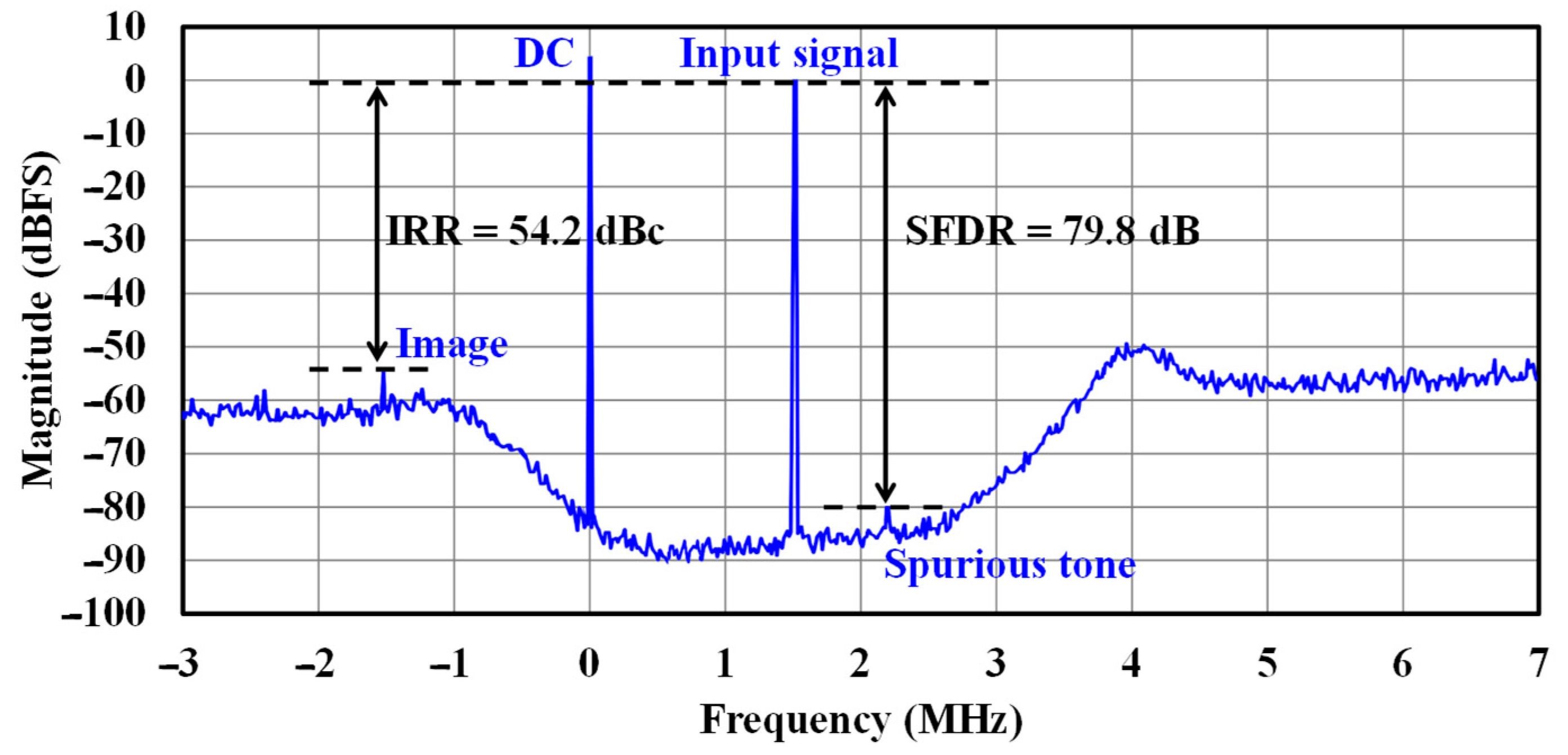
| IRR (dBc) | 54.2 | N/A | N/A | 32 | N/A | N/A | 59.3 | 59.6 |
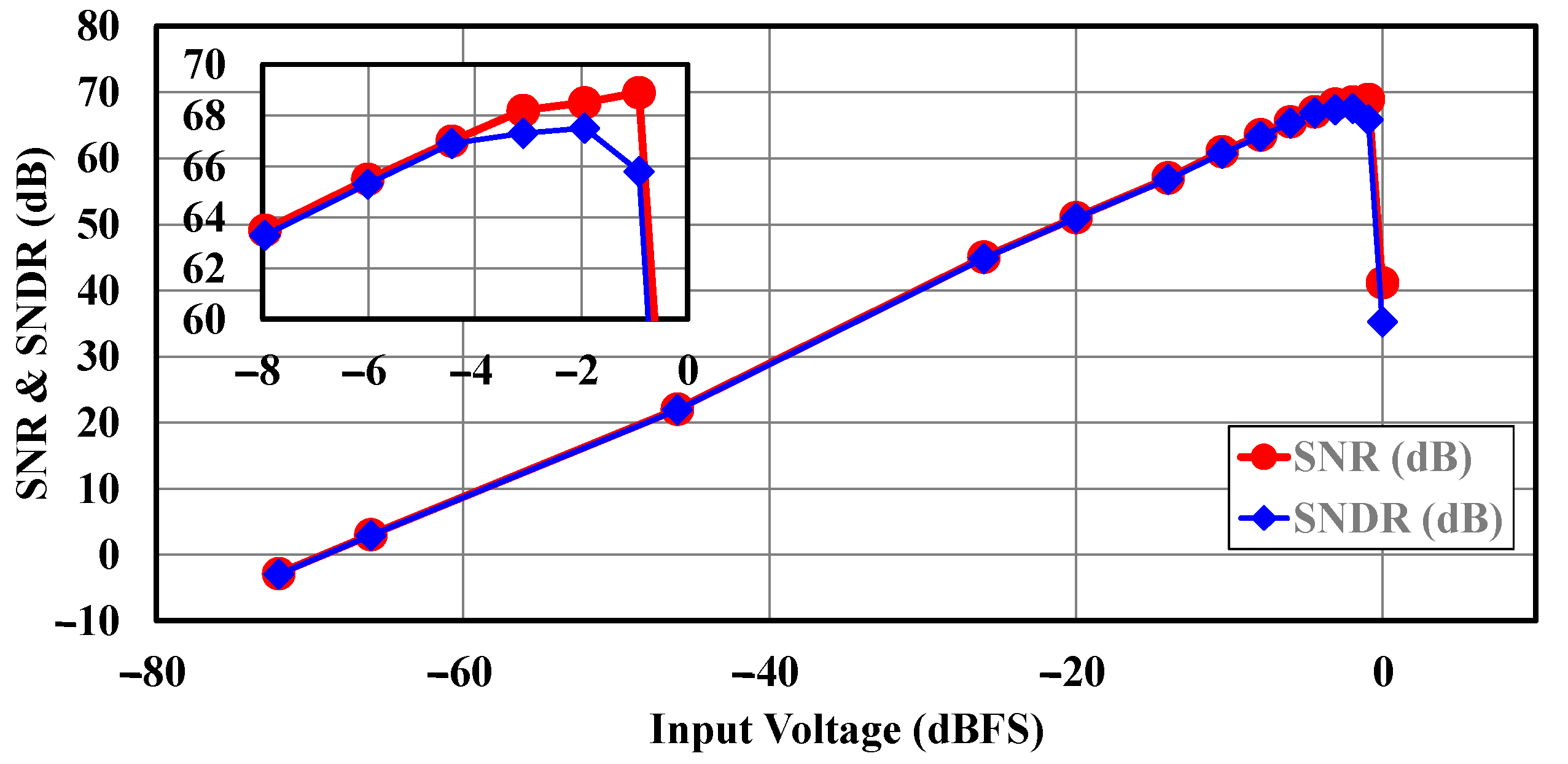
| DR (dB) | 70.3 | 102.6 | 94.1 | 66 | N/A | 120.3 | 64 | 74.3 |
| SNDR (dB) | 67.5 | 98.6 | 89.3 | 65.2 | N/A | 118.1 | 62.1 | 62.9 |
| SNR (dB) | 68.9 | 101.5 | 91.9 | N/A | N/A | 119.1 | 64.5 | 64.4 |
| Supply Voltage (V) | 1.0 | 1.8 | 1.5 | 1.04 | N/A | 1.8 | 1.8 | 1.2 |
| ADC Power (mW) | 0.81 | 1.3 | 0.004 | * 1.2 | 2.4 | 0.28 | * 25.4 | 4.2 |
| ADC Area (mm2) | 0.145 | 0.648 | 0.75 | 0.18 | 0.24 | 0.25 | 0.73 | 0.39 |
| ** FOMS (dB) | 164.3 | 171.5 | 177.1 | 158.2 | N/A | 185.8 | 155.1 | 165.1 |
| ** FOMW (fJ/conv.) | 103.2 | 934.2 | 104.8 | 201.7 | N/A | 213.1 | 369.8 | 368.1 |
Disclaimer/Publisher’s Note: The statements, opinions and data contained in all publications are solely those of the individual author(s) and contributor(s) and not of MDPI and/or the editor(s). MDPI and/or the editor(s) disclaim responsibility for any injury to people or property resulting from any ideas, methods, instructions or products referred to in the content. |
© 2025 by the author. Licensee MDPI, Basel, Switzerland. This article is an open access article distributed under the terms and conditions of the Creative Commons Attribution (CC BY) license (https://creativecommons.org/licenses/by/4.0/).
Share and Cite
Kim, N.-S. A Low-Power Complementary Metal-Oxide-Semiconductor Receiver with Quadrature Bandpass Continuous-Time Delta–Sigma Analog-to-Digital Converter for IoT Applications. Sensors 2025, 25, 1748. https://doi.org/10.3390/s25061748
Kim N-S. A Low-Power Complementary Metal-Oxide-Semiconductor Receiver with Quadrature Bandpass Continuous-Time Delta–Sigma Analog-to-Digital Converter for IoT Applications. Sensors. 2025; 25(6):1748. https://doi.org/10.3390/s25061748
Chicago/Turabian StyleKim, Nam-Seog. 2025. "A Low-Power Complementary Metal-Oxide-Semiconductor Receiver with Quadrature Bandpass Continuous-Time Delta–Sigma Analog-to-Digital Converter for IoT Applications" Sensors 25, no. 6: 1748. https://doi.org/10.3390/s25061748
APA StyleKim, N.-S. (2025). A Low-Power Complementary Metal-Oxide-Semiconductor Receiver with Quadrature Bandpass Continuous-Time Delta–Sigma Analog-to-Digital Converter for IoT Applications. Sensors, 25(6), 1748. https://doi.org/10.3390/s25061748