

Low-Jitter Clock Receivers for Fast Timing Applications


Abstract
1. Introduction
2. Materials and Methods
2.1. Technology Selection
2.2. Receiver Architecture
2.2.1. LVDS
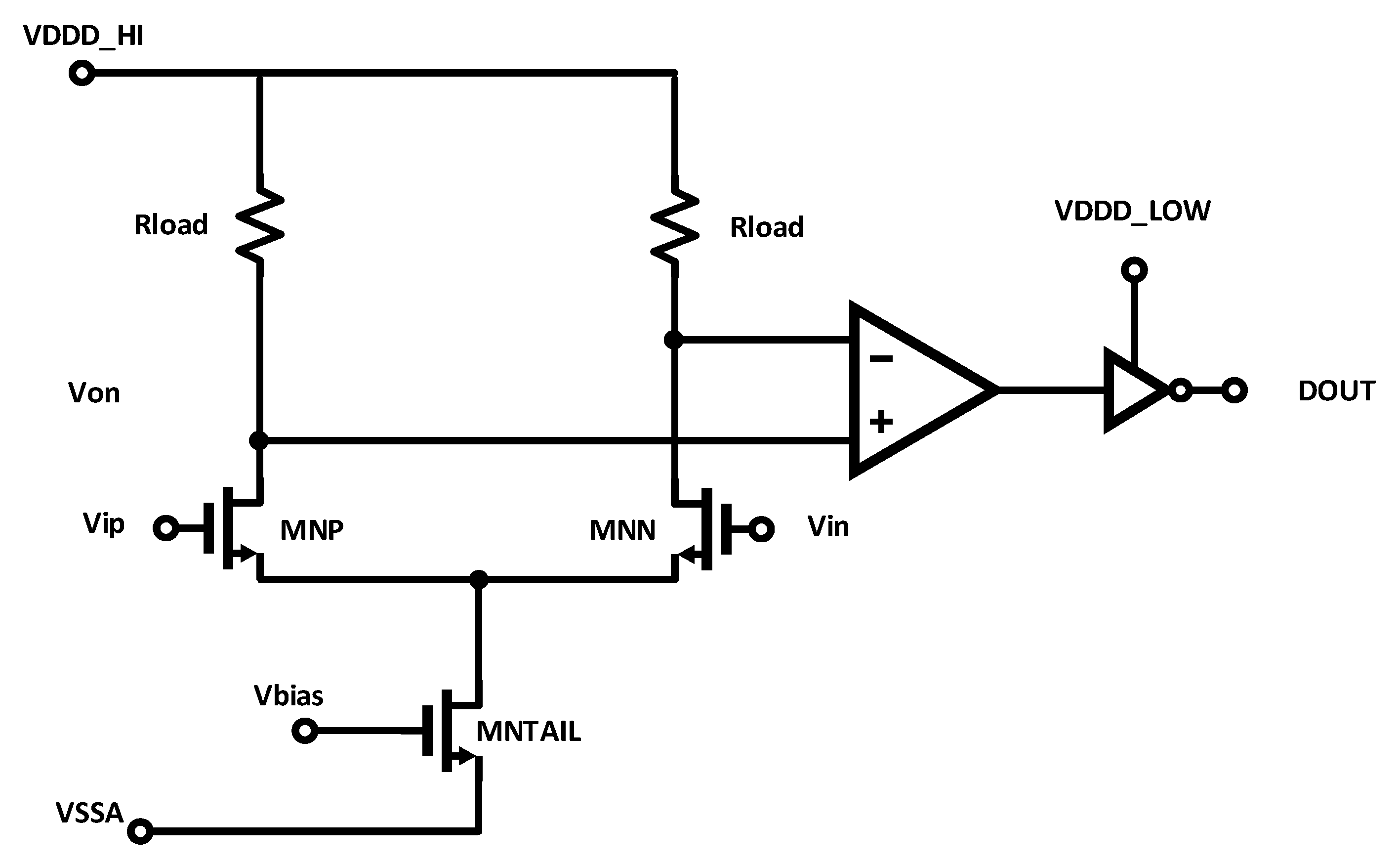
2.2.2. Differential-Pair with Resistive Load
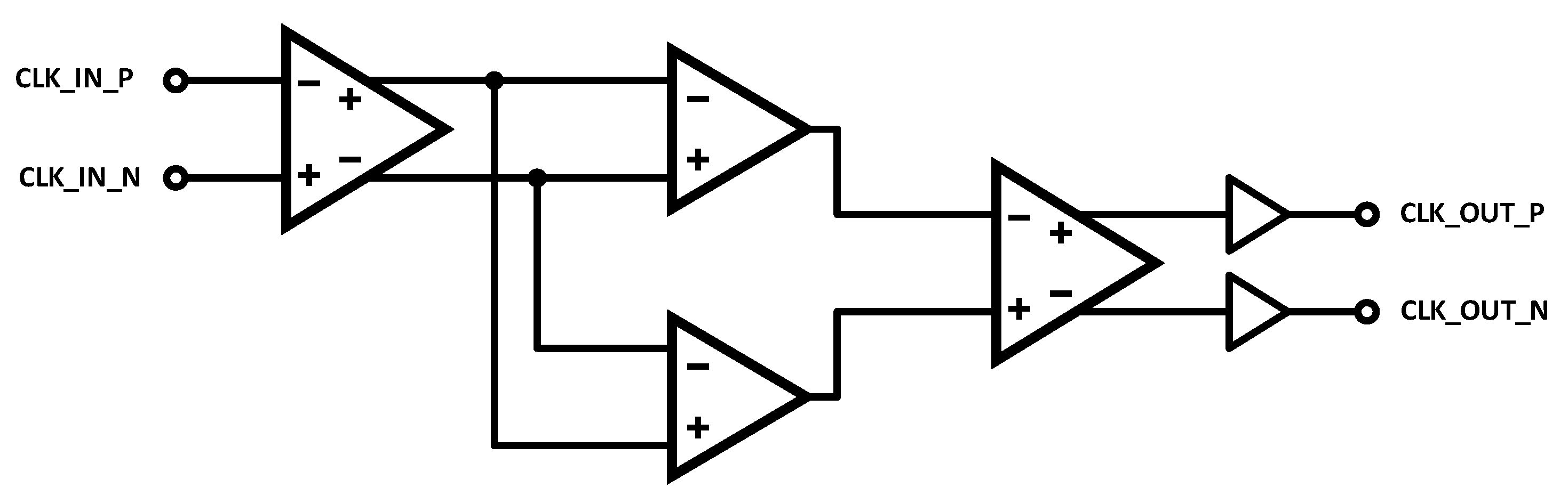
2.2.3. Multi-Stage Amplification
2.2.4. Clock Distribution
2.2.5. Simulated Comparison
2.3. Prototype
2.3.1. Schematic Design
2.3.2. Layout Design
2.3.3. Transient Jitter Simulation
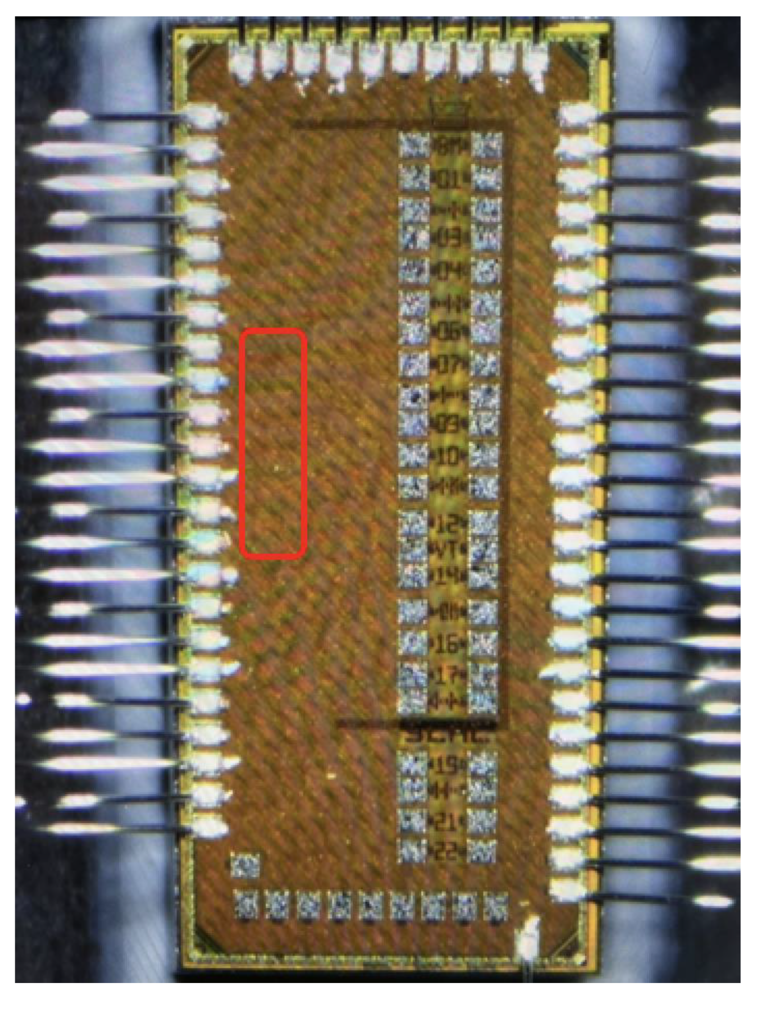
2.3.4. Die Photo
3. Results
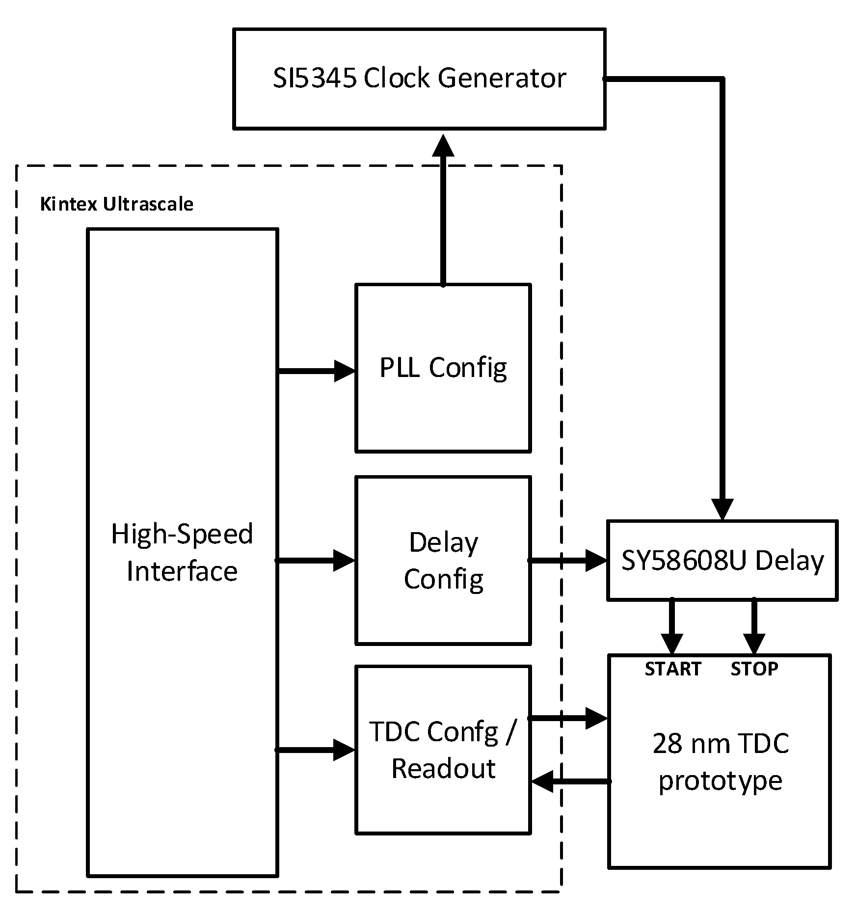
3.1. Test Setup
3.2. Measured Results
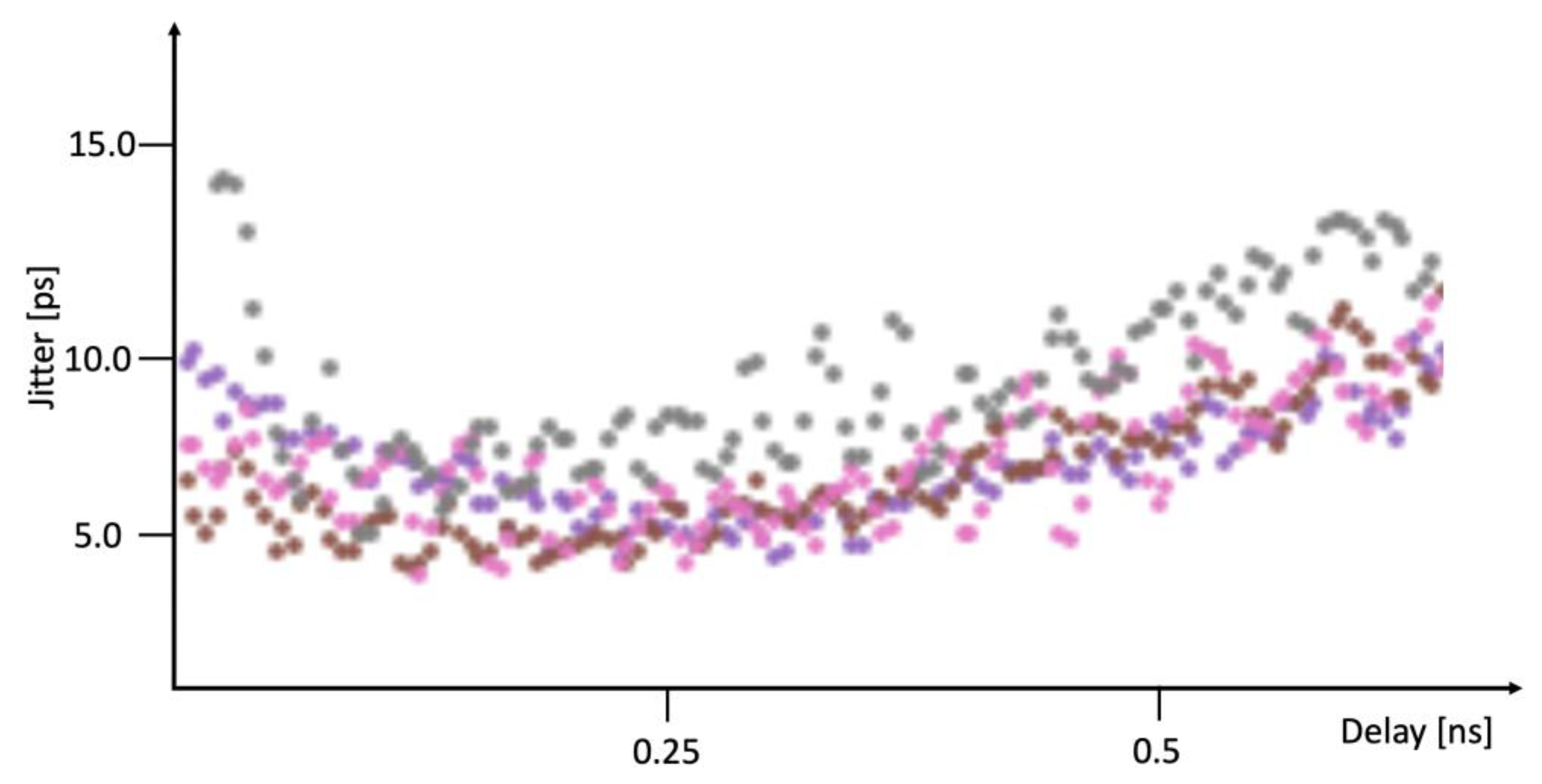
Time-of-Arrival Jitter
3.3. Comparison with Other Work
4. Conclusions
Author Contributions
Funding
Institutional Review Board Statement
Informed Consent Statement
Data Availability Statement
Acknowledgments
Conflicts of Interest
Abbreviations
| CMOS | Complementary Metal Oxide Semiconductor |
| CMS | Compact Muon Solenoid |
| DAC | Digital-to-Analog Converter |
| DPRL | Differential Pair with Resistive Load |
| FCC | Future Circular Collider |
| FMC | FPGA Mezzanine Card |
| FPGA | Field Programmable Gate Array |
| FOM | Figure-of-Merit |
| HEP | High-Energy Physics |
| HL-LHC | High-Luminosity Large Hadron Collider |
| ILC | International Linear Collider |
| LGAD | Low-Gain Avalanche Detector |
| LVDS | Low-Voltage Differential Signaling |
| PET | Positron Emission Tomography |
| PLL | Phase-Locked Loop |
| PRBS | Pseudo-Random Bit Sequence |
| SiPM | Silicon Photomultipliers |
| TDC | Time-to-Digital Converter |
| TOA | Time-of-Arrival |
| TOF | Time-of-Flight |
References
- Particle Physics Project Prioritization Panel. Report of the Particle Physics Project Prioritization Panel; US Department of Energy: Washington, DC, USA, 2024. [Google Scholar]
- Abada, A.; Abbrescia, M.; Abdussalam, S.S.; Abdyukhanov, I.; Abelleira Fernandez, J.; Abramov, A.; Aburaia, M.; Acar, A.O.; Adzic, P.R.; Agrawal, P.; et al. FCC-hh: The Hadron Collider. Eur. Phys. J. Spec. Top. 2019, 228, 755–1107. [Google Scholar] [CrossRef]
- Accettura, C.; Adams, D.; Agarwal, R.; Ahdida, C.; Aimè, C.; Amapane, N.; Amorim, D.; Andreetto, P.; Anulli, F.; Appleby, R.; et al. Towards a muon collider. Eur. Phys. J. C 2023, 83, 864. [Google Scholar] [CrossRef]
- Azzi, P.; Perez, E. Exploring requirements and detector solutions for FCC-ee. Eur. Phys. J. Plus 2021, 136, 1195. [Google Scholar] [CrossRef]
- Nadig, V.; Gundacker, S.; Herweg, K.; Naunheim, S.; Schug, D.; Weissler, B.; Schulz, V. ASICs in PET: What we have and what we need. EJNMMI Phys. 2025, 12, 16. [Google Scholar]
- Yeom, J.Y.; Spanoudaki, V.; Levin, C.S. Silicon photomultiplier-based detector array for TOF PET. In Proceedings of the 2011 IEEE Nuclear Science Symposium Conference Record, Valencia, Spain, 23–29 October 2011; pp. 2415–2417. [Google Scholar]
- Lewellen, T.K. Time-of-flight PET. Semin. Nucl. Med. 1998, 28, 268–275. [Google Scholar] [CrossRef]
- Di Francesco, A.; Bugalho, R.; Oliveira, L.; Rivetti, A.; Rolo, M.; Silva, J.C.; Varela, J. TOFPET 2: A high-performance circuit for PET time-of-flight. Nucl. Instrum. Methods Phys. Res. Sect. A Accel. Spectrometers Detect. Assoc. Equip. 2016, 824, 194–195. [Google Scholar] [CrossRef]
- Moffat, N.; Bates, R.; Bullough, M.; Flores, L.; Maneuski, D.; Simon, L.; Tartoni, N.; Doherty, F.; Ashby, J. Low Gain Avalanche Detectors (LGAD) for particle physics and synchrotron applications. J. Instrum. 2018, 13, C03014. [Google Scholar] [CrossRef]
- Cartiglia, N.; Arcidiacono, R.; Borghi, G.; Boscardin, M.; Costa, M.; Galloway, Z.; Fausti, F.; Ferrero, M.; Ficorella, F.; Mandurrino, M.; et al. LGAD designs for Future Particle Trackers. Nucl. Instrum. Methods Phys. Res. Sect. A Accel. Spectrometers Detect. Assoc. Equip. 2020, 979, 164383. [Google Scholar] [CrossRef]
- Huang, X.; Alvarez, I.V.; Arcidiacono, R.; Chlebana, F.; Duarte, J.; Evdokimov, O.; Flowers, Z.B.; Fu, T.; Gallinaro, M.; Garcia, M.; et al. The testing and performance of the ETROC2 for CMS MTD Endcap Timing Layer (ETL) upgrade. In Proceedings of the 2024 IEEE Nuclear Science Symposium (NSS), Medical Imaging Conference (MIC) and Room Temperature Semiconductor Detector Conference (RTSD), Tampa, FL, USA, 26 October–2 November 2024; pp. 1–2. [Google Scholar]
- Bohon, J.; Gonzalez, E.; Grace, C.; Harris, C.T.; Jacobsen, B.; Kachiguine, S.; Kim, D.; Macarthur, J.; Martinez-Mckinney, F.; Mazza, S.; et al. Use of diamond sensors for a high-flux, high-rate X-ray pass-through diagnostic. J. Synchrotron Radiat. 2022, 29, 595–601. [Google Scholar] [CrossRef]
- Cesaroni, S.; Angelone, M.; Apruzzese, G.; Bombarda, F.; Gabellieri, L.; Marinelli, M.; Milani, E.; Palomba, S.; Pucella, G.; Romano, A.; et al. CVD diamond photodetectors for FTU plasma diagnostics. Fusion Eng. Des. 2021, 166, 112323. [Google Scholar] [CrossRef]
- Narku-Tetteh, N.; Titriku, A.; Palermo, S. A 15b, Sub-10ps resolution, low dead time, wide range two-stage TDC. In Proceedings of the 57th IEEE Midwest Symposium on Circuits and Systems, College Station, TX, USA, 3–8 August 2014; pp. 13–16. [Google Scholar]
- Xiang, G.; Klumperink, E.A.M.; Geraedts, P.F.J.; Nauta, B. Jitter Analysis and a Benchmarking Figure-of-Merit for Phase-Locked Loops. IEEE Trans. Circuits Syst. II Express Briefs 2009, 56, 117–121. [Google Scholar] [CrossRef]
- Termo, G.; Borghello, G.; Faccio, F.; Michelis, S.; Koukab, A.; Sallese, J.M. Radiation response of 28 nm CMOS transistors at high proton and neutron fluences for high energy physics applications. Nucl. Instrum. Methods Phys. Res. Sect. A Accel. Spectrometers Detect. Assoc. Equip. 2024, 1065, 169497. [Google Scholar] [CrossRef]
- Boni, A.; Pierazzi, A.; Vecchi, D. LVDS I/O interface for Gb/s-per-pin operation in 0.35-μm CMOS. IEEE J. Solid-State Circuits 2001, 36, 706–711. [Google Scholar] [CrossRef]
- Gray, P.; Hurst, P.; Lewis, S.; Meyer, R. Analysis and Design of Analog Integrated Circuits, 6th ed.; Wiley: Hoboken, NJ, USA, 2024. [Google Scholar]
- Razavi, B. Principles of Data Conversion System Design; Wiley-IEEE: Hoboken, NJ, USA, 1995. [Google Scholar]
- Mo, X.; Wu, J.; Wary, N.; Carusone, T.C. Design Methodologies for Low-Jitter CMOS Clock Distribution. IEEE Open J. Solid-State Circuits Soc. 2021, 1, 94–103. [Google Scholar] [CrossRef]
- Krieger, A.; Caisley, K.; Garcia-Sciveres, M.; Grace, C.; Heim, T.; Zhang, Z. Characterization of the BigRock 28 nm fast timing Analog Front End. J. Instrum. 2024, 19, C05012. [Google Scholar] [CrossRef]
- Mendez, J.; Pena Perez, A.; Dragone, A.; Markovic, B. Design update and characterization of sub-10ps TDC ADC in 28nm for future 4D trackers. In Proceedings of the Topical Workshop on Electronics for Particle Physics, Glasgow, UK, 30 September–4 October 2024. [Google Scholar]
- Markovic, B.; England, T.; Gupta, A.; Braga, D.; Mendez, J. Design of 28nm readout ASIC prototype for 3D-integrated LGAD sensors. In Proceedings of the Topical Workshop on Electronics for Particle Physics, Glasgow, UK, 30 September–4 October 2024. [Google Scholar]
- Rabaey, J.; Chandrakasan, A.; Nikolic, B. Digital Integrated Circuits, a Design Perspective, 2nd ed.; Prentice Hall: Saddle River, NJ, USA, 2002. [Google Scholar]
- Kossel, M.; Menolfi, C.; Weiss, J.; Buchmann, P.; Von Bueren, G.; Rodoni, L.; Morf, T.; Toifl, T.; Schmatz, M. A T-Coil-Enhanced 8.5 Gb/s High-Swing SST Transmitter in 65 nm Bulk CMOS With $≪ -$16 dB Return Loss Over 10 GHz Bandwidth. IEEE J. Solid-State Circuits 2008, 43, 2905–2920. [Google Scholar] [CrossRef]
- Sklar, B.; Harris, F. Digital Communications: Fundamentals and Applications, 3rd ed.; Pearson: London, UK, 2020. [Google Scholar]
- Wu, K.; Xie, Y.; Tao, S.; Zhang, Z.; Ning, N.; Li, J.; Yu, Q. A 3–5 GHz, 108fs-RMS jitter, clock receiver circuit for time-interleaved ADCs with a sampling rate of 4 GS/s. Microelectron. J. 2023, 139, 105889. [Google Scholar] [CrossRef]
- Chae, J.-H.; Ko, H.; Park, J.; Kim, S. A Quadrature Clock Corrector for DRAM Interfaces, with a Duty-Cycle and Quadrature Phase Detector Based on a Relaxation Oscillator. IEEE Trans. Very Large Scale Integr. (VLSI) Syst. 2019, 27, 978–982. [Google Scholar] [CrossRef]
- Park, H.; Sim, J.; Choi, Y.; Choi, J.; Kwon, Y.; Park, S.; Park, G.; Chung, J.; Kim, K.-M.; Jung, H.-K.; et al. A 1.3–4-GHz Quadrature-Phase Digital DLL Using Sequential Delay Control and Reconfigurable Delay Line. IEEE J. Solid-State Circuits 2021, 56, 1886–1896. [Google Scholar] [CrossRef]
- Liu, M.; Jiang, Y.; Dong, S.; Zhu, Z.; Yang, Y. A low-jitter wide-range duty cycle corrector for high-speed high-precision ADC. Microelectron. J. 2015, 46, 332–342. [Google Scholar]
- Kim, K.M.; Hwang, S.; Song, J.; Kim, C. An 11.2-Gb/s LVDS Receiver with a Wide Input Range Comparator. IEEE Trans. Very Large Scale Integr. (VLSI) Syst. 2014, 22, 2156–2163. [Google Scholar] [CrossRef]


| Circuit | Frequency [GHz] | rms Jitter [ps] | Power [mW] |
|---|---|---|---|
| LVDS | 5.0 | 12.2 | 1.1 |
| Multi-stage | 5.0 | 4.9 | 2.1 |
| DPRL | 5.0 | 1.2 | 1.8 |
| References | Process | Frequency [GHz] | rms Jitter [ps] | Power [mW] | FOM [dB] |
|---|---|---|---|---|---|
| [27] | 28 | 3.5 | 0.1 | 10 | −15.4 |
| [28] | 55 | 3.0 | 2.14 | 2.1 | 5.06 |
| [29] | 28 | 4.0 | 1.82 | 1.9 | 1.97 |
| [30] | 65 | 0.2 | 0.2 | 1.9 | −4.20 |
| [31] | 130 | 11.2 | 58.9 | 1.6 | 2.69 |
| This Work | 28 | 5.0 | 2.25 1 | 1.8 | 2.61 |
Disclaimer/Publisher’s Note: The statements, opinions and data contained in all publications are solely those of the individual author(s) and contributor(s) and not of MDPI and/or the editor(s). MDPI and/or the editor(s) disclaim responsibility for any injury to people or property resulting from any ideas, methods, instructions or products referred to in the content. |
© 2025 by the authors. Licensee MDPI, Basel, Switzerland. This article is an open access article distributed under the terms and conditions of the Creative Commons Attribution (CC BY) license (https://creativecommons.org/licenses/by/4.0/).
Share and Cite
Grace, C.; Garcia-Sciveres, M.; Heim, T.; Krieger, A. Low-Jitter Clock Receivers for Fast Timing Applications. Sensors 2025, 25, 2284. https://doi.org/10.3390/s25072284
Grace C, Garcia-Sciveres M, Heim T, Krieger A. Low-Jitter Clock Receivers for Fast Timing Applications. Sensors. 2025; 25(7):2284. https://doi.org/10.3390/s25072284
Chicago/Turabian StyleGrace, Carl, Maurice Garcia-Sciveres, Timon Heim, and Amanda Krieger. 2025. "Low-Jitter Clock Receivers for Fast Timing Applications" Sensors 25, no. 7: 2284. https://doi.org/10.3390/s25072284
APA StyleGrace, C., Garcia-Sciveres, M., Heim, T., & Krieger, A. (2025). Low-Jitter Clock Receivers for Fast Timing Applications. Sensors, 25(7), 2284. https://doi.org/10.3390/s25072284