Abstract
Due to high responsivity and wide spectral sensitivity, metal halide perovskite photodiodes have a wide range of applications in the fields of visible light and near-infrared photodetection. Specific detectivity is an important quality factor for high-performance perovskite-based photodiodes, while one of the keys to achieving high detectivity is to reduce dark current. Here, 3-fluoro phenethylammonium iodide (3F-PEAI) was used to passivate the perovskite surface and form the two-dimensional (2D) perovskite on the three-dimensional (3D) perovskite surface. The as-fabricated passivated perovskite photodiodes with 2D/3D hybrid-dimensional perovskite heterojunctions showed two orders of magnitude smaller dark current, larger open circuit voltage and faster photoresponse, when compared to the control perovskite photodiodes. Meanwhile, it maintained almost identical photocurrent, achieving a high specific detectivity up to 2.4 × 10¹² Jones and over the visible-near-infrared broadband photodetection. Notably, the champion photoresponsivity value of 0.45 A W−1 was achieved at 760 nm. It was verified that the 2D capping layers were able to suppress trap states and accelerate photocarrier collection. This work demonstrates strategic passivation of surface iodine vacancies, offering a promising pathway for developing ultrasensitive and low-power consumption photodetectors based on metal halide perovskites.
1. Introduction
In recent years, the organic-inorganic hybrid perovskites have brought a breakthrough in the optoelectronic applications, such as solar cells [1,2], light-emitting diodes [3,4], and photodetectors [5,6,7]. Their large optical absorption coefficient, long carrier diffusion length, high carrier mobility, and tunable bandgap enable photodetectors to show high photoresponsivity and fast response/recovery for various wavelength detection [8,9,10,11,12,13]. Notably, one of the key quality factors for a sensitive photodetector is specific detectivity (D*), which is proportional to the reciprocal of the noise-equivalent power (NEP) and is determined by the ratio of the responsivity over noise current [14]. Typically, the reverse bias dark current (Idark) contributes to the major noise current in realistic photodiodes [15,16,17,18]. However, to date, the solution-treated perovskite photodiodes have still suffered from relatively high Idark, lowering D* and thus restricting detection of weak light signals. Thereby, reducing Idark is essential to facilitate their photodetection applications.
As reported, Idark in photodiodes can mainly originate from the defects present within the perovskites and the minority charges injected from the electrodes under reverse bias [19,20]. Thus, the main strategies to suppress Idark can be categorized into two groups: refinement of device configuration design and improvement of material crystal quality of light absorbing layers [21]. For example, hole/electron blocking layers and edge-covering layers have been introduced [20,22]. Fang et al. replaced poly(3,4-ethylenedioxythiophene):poly(styrenesulfonate)(PEDOT:PSS)withN4,N4′-bis(4-(6-((3-ethyloxetan-3-yl)methoxy)hexyl)phenyl)-N4,N4′-diphenylbiphenyl-4,4′-diamine (OTPD) to increase electron injection barrier from 1.1 eV to 2.5 eV and thus succeeded in suppressing Idark [23]. Shen et al. created a large hole injection barrier (>2 eV) between the metal copper (Cu) electrode and the buckminsterfullerene (C60) layer by optimizing the contact interface [20]. Gelinck et al. developed inherent mechanisms about the effect of charge blocking layers to reduce Idark and lowered Idark in near-infrared perovskite photodiodes by suppressing carrier injection and interfacial carrier generation [24]. In addition, efforts have also been made to improve the crystal quality of the absorber layer through various strategies including doping [25,26], thin film processing engineering [27] and surface passivation [28]. Zhao et al. introduced thioacetamide (C2H5NS) to the CsPbBr3 film. The uncoordinated Pb2+ defects on the surface were passivated, suppressing nonradiative recombination and accelerating carriers extraction [29]. Jiang et al. used organic halide salt phenethylammonium iodide (PEAI) on perovskite films, and they inferred that the PEAI coating on the perovskite layer fills the iodine vacancies on the surface and at the grain boundary, resulting in passivation of the surface defects [30]. Inspired by the previous studies, the way guaranteeing both good crystal quality and optimized energy-band alignment can be very effective for sensitive perovskite photodiodes.
Two-dimensional (2D) metal halide compounds are a class of layered materials with atomic-level thicknesses, typically composed of metal cations and halogen anions (e.g., Cl−, Br−, I−). Due to their unique electronic, optical, and structural properties, these materials have attracted extensive attention in the fields of optoelectronics, energy and catalysis in recent years [31]. Among them, 2D perovskites are the most studied materials due to their resistance to oxygen and moisture compared to three-dimensional (3D) perovskites. In addition, two-dimensional/three-dimensional (2D/3D) hybrid-dimensional perovskite heterojunctions have also attracted strong interest, since the 2D layer plays a crucial role not only in passivating surface defects but also in facilitating carrier extraction [32,33,34,35]. Lai et al. ensured the reduction of surface iodine vacancy-induced trap states and favorable energy level alignment at the perovskite/hole transport layer interface by introducing a mixed-phase 2D perovskite to 3D perovskite [36]. Applying organic salts, which can form 2D perovskite through reaction with 3D perovskite, to a 3D surface, in principle, should allow us to decrease Idark by reducing undesirable defects and improving energy-band alignment quality.
In this study, the 2D perovskite was introduced to the 3D perovskite/electron transport layer (ETL) interface using 3F-PEAI post-processing. To reduce electron blocking in the 2D perovskite between the 3D perovskite and the ETL, the 2D perovskite containing n ≥ 3 layers was selected, which possessed closer conduction band minimum (CBM) to the 3D perovskite. After 2D post-treatment, the scanning electron microscopy (SEM) and atomic force microscopy (AFM) images showed smoother surface morphology and the photoluminescence (PL) spectra showed the higher emission intensity. These results suggest that unwanted defects were effectively mitigated. By using surface defect passivation of the molecules, the Idark of the photodiode was significantly reduced and a competitive D* of 2.4 × 10¹² Jones was achieved. Evidently, this study demonstrated that defect passivation in perovskite thin films is one of the keys to achieving optimal performance of perovskite photodiodes.
2. Materials and Methods
2.1. Material Synthesis
Cesium iodide (CsI, >99.5%), lead iodide (PbI2, >99.5%), formamidinium iodide (FAI, >99.5%), methylammonium iodide (MAI, >99.5%), 3-fluoro phenethylammonium iodide (3F-PEAI, >99.5%), bathocuproine (BCP), Nickel oxide (NiOx, 2.5 wt.%), and poly(3,4-ethylenedioxythiophene):poly(styrenesulfonate) (PEDOT:PSS) were purchased from Xi’an Polymer Light Technology (Xi’an, China). Fullerene (C60) (99.5%), dimethyl sulfoxide (DMSO, anhydrous), dimethylformamide (DMF, anhydrous), isopropyl alcohol (IPA, anhydrous), and chlorobenzene (CB, anhydrous) were obtained from Aladdin (Tokyo, Japan). Indiumtin oxide (ITO) coated glasses (~15 Ω sq−1) were purchased from GuoKe JingYan (Tianjin) Technology (Tianjin, China). All of the chemicals and materials were used as purchased without further purification.
2.2. Device Fabrication
The ITO substrates were sequentially cleaned with detergent, deionized water, acetone, IPA, and ethanol by sonication treatment for 15 min in each step. After N2 drying, the ITO substrates were treated with O2 plasma for 15 min. For devices with EBL of PEDOT:PSS, the PEDOT:PSS layer was deposited by spin-coating at 4000 r.p.m. for 40 s and then annealed at 150 °C for 15 min. For devices with EBL of NiOx, the NiOx layer was deposited by spin-coating at 5000 r.p.m. for 30 s and then annealed at 150 °C for 30 min. The 1.4 M FA0.95Cs0.05PbI3 perovskite precursor was prepared by dissolving 18.2 mg CsI, 645.4 mg PbI2, and 228.4 mg FAI in mixed solvents of DMF and DMSO (v/v, 4/1) stirring overnight. The precursor solution was spin-coated on the ITO/NiOx substrates at 2000 r.p.m. for 10 s and then at 4000 r.p.m. for 40 s. During the second spin-coating step, 150 µL CB was dropped onto the perovskite film at 5 s before the end of the programme. The wet perovskite films were annealed at 100 °C for 30 min. For post-treated films, 2D ligand solution was prepared by dissolving 3F-PEAI (1 mg mL−1) and MAI (0.5 mg mL−1) in mixed solvents of IPA and DMF (v/v, 200/1). The 2D layer was fabricated by depositing the 2D ligand solution (150 µL) onto the perovskite film surface. After deposition, the film was spun at a rate of 4000 r.p.m. for 40 s with a 4000 r.p.m. per second acceleration. The film was then annealed at 100 °C for 5 min. Then ETL C60 (40 nm), BCP (8 nm) and Ag (70 nm) electrode were deposited by thermal evaporation in order.
2.3. Characterization and Measurement
The X-ray diffraction (XRD) patterns were performed using D2 PHASER (Bruker, Billerca, MA, USA). The steady-state PL and AFM measurements were performed using WITec Alpha300 Raman (WITec, Ulm, Germany). The morphology of the perovskite films was determined by SEM using Zeiss Sigma500 (Zeiss, Munich, Germany). The I−V curves of the photodiodes were obtainedusing Keithley 4200 (Keithley, Beaverton, OR, USA). Light sources with varied wavelengths were supplied using NKT Photonics SuperK SELECT (NKT Photonics, Copenhagen, Denmark). The response speed of the photodiodes was evaluated by recording the transient signal to light pulses with variable frequenciesusing FS-PRO (Primaries, Shanghai, China). The light pulses were generated by a laser diode of 650 nm that was connected to a signal generator.
3. Results and Discussion
Considering the organic-inorganic hybrid perovskite FA0.95Cs0.05PbI3 has good thermal stability and suitable bandgap, it was selected as the absorber layer of a near-infrared photodetector in this work [37]. The pristine FA0.95Cs0.05PbI3 perovskite films were prepared by a one-step spin-coating method. Due to dipole moment and hydrophobic nature, the fluorinated ammonium salts are effective additives to improve device performance. In addition, they are able to produce 2D/3D heterojunctions containing more n = 3 2D perovskite than those formed by PEAI [38]. Since the fluorinated ammonium salts are effective additives to improve the device performance possibly due to their dipole moment and hydrophobic nature, 2D 3F-PEAI was chosen to spin-coat on the top of the 3D perovskite film for cation exchange. It enabled the passivation of defects on the 3D perovskite surface [39,40,41,42]. Notably, introducing a small amount of DMF and MAI to precursor solution of 3F-PEAI was able to improve device performance due to better energy-band alignment [38]. Thus, this precursor solution was spin-coated onto the 3D perovskite film to prepare 2D perovskite layers, forming 2D/3D hybrid-dimensional perovskite heterojunctions.
To examine the microstructure passivation effects of the as-synthesized perovskite films, SEM and AFM characterization were carried out. As shown in Figure 1a,b, the control film without 2D layer exhibited many distinct grain boundaries, possessing a large root-mean-square (RMS) roughness of 36 nm. In comparison, the post-treated film, containing the 2D/3D hybrid-dimensional heterojunctions, exhibited fewer grain boundaries and the smaller RMS roughness value down to 21 nm in Figure 1c,d, and the surface morphology became smoother. Evidently, it can be inferred that introduction of 2D perovskites was able to passivate surface and suppress grain boundaries, which can potentially reduce the recombination loss. Figure 1e illustrates the characteristic X-Ray diffraction (XRD) patterns of the control and the passivated perovskite films, while the 2D phase cannot be observed directly in the XRD result. This was consistent with the previously reported results [19,36].
Furthermore, to verify the existence of 2D perovskite on the surface, steady-state PL measurements were performed. The normalized PL spectra of the control and the passivated perovskite films are shown in Figure 1f. In addition to the PL peaks from 3D perovskites at around 800 nm, PL peaks associated with n = 2, 3, and 4 were also observed in the passivated films, indicating the presence of the 2D perovskites on the surface [19,43]. Meanwhile, the stronger PL peak intensity of the passivated perovskite films in Figure 1g indicated the trap-assisted carrier recombination on the surface can be effectively suppressed, further illustrating the reduced surface defects.

Figure 1.
(a,b) AFM and SEM images of the control perovskite film; (c,d) AFM and SEM images of the passivated perovskite film; (e) the XRD patterns of the control and the passivated perovskite films. (f) Normalized steady-state PL spectra of the control and the passivated perovskite films, showing 2D features after passivation; (g) PL spectra of the control and passivated perovskite thin films. Subsequently, the perovskite photodiodes were fabricated with the inverted structure (that is, positive-intrinsic-negative, or PIN) because of the generally better stability [44,45,46,47]. The perovskite photodiodes were fabricated on the glass substrates with patterned ITO electrodes on top, as shown in Figure 2a. The ITO electrodes were first coated with an electron-blocking layer (EBL) of NiOx, and then FA0.95Cs0.05PbI3 perovskite was prepared to form absorber layer, followed by the sequential deposition of fullerene (C60)/BCP as ETL, and finally the Ag electrode was deposited. The crossover ITO and Ag electrodes determined the active region area to be 0.02 cm2.
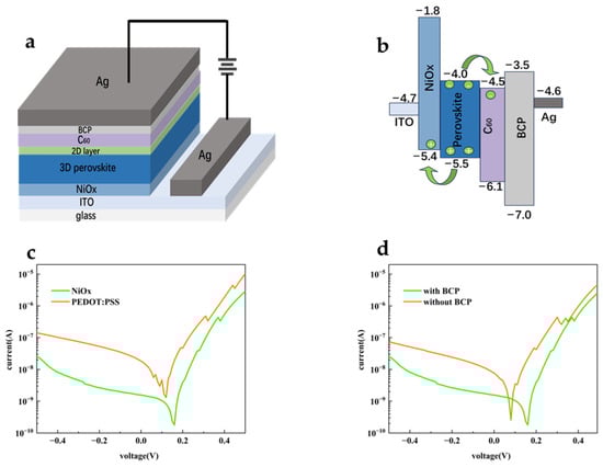
Figure 2.
(a) Schematic device structure of the perovskite photodiode, fabricated with the inverted structure; (b) The energy level diagram of the perovskite photodiode; (c) Idark vs. applied voltages for perovskite photodiodes using different EBLs of PEDOT:PSS and NiOx, respectively; (d) Idark vs. applied voltages for perovskite photodiodes with and without BCP.
Figure 1.
(a,b) AFM and SEM images of the control perovskite film; (c,d) AFM and SEM images of the passivated perovskite film; (e) the XRD patterns of the control and the passivated perovskite films. (f) Normalized steady-state PL spectra of the control and the passivated perovskite films, showing 2D features after passivation; (g) PL spectra of the control and passivated perovskite thin films. Subsequently, the perovskite photodiodes were fabricated with the inverted structure (that is, positive-intrinsic-negative, or PIN) because of the generally better stability [44,45,46,47]. The perovskite photodiodes were fabricated on the glass substrates with patterned ITO electrodes on top, as shown in Figure 2a. The ITO electrodes were first coated with an electron-blocking layer (EBL) of NiOx, and then FA0.95Cs0.05PbI3 perovskite was prepared to form absorber layer, followed by the sequential deposition of fullerene (C60)/BCP as ETL, and finally the Ag electrode was deposited. The crossover ITO and Ag electrodes determined the active region area to be 0.02 cm2.
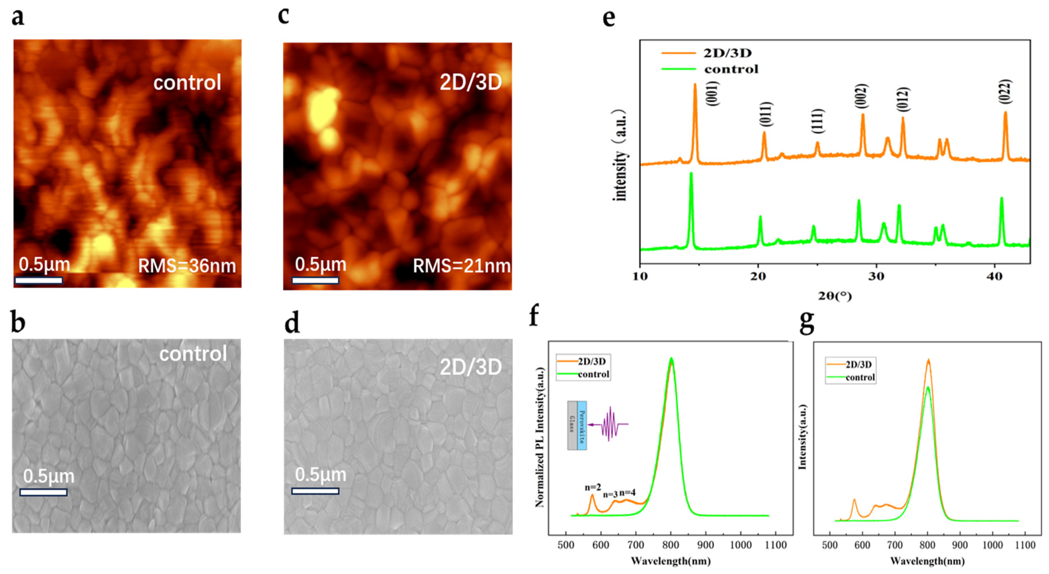
Figure 2b displays the energy level diagram of the perovskite photodiode. NiOx/FA0.95Cs0.05PbI3/C60 type II heterojunctions were formed, which can potentially mitigate the interfacial complexation and promote the separation of photogenerated carriers. As displayed in Figure 2c, the Idark of the devices was greatly reduced compared to the devices using PEDOT:PSS. Compared with the common EBL of PEDOT:PSS, the higher electron injection barrier at the ITO/NiOx interface can significantly block the minority electron injection from ITO under reverse bias. In addition, the deep highest occupied molecular orbital (HOMO) of BCP achieved hole blocking from the silver electrode. As expected, Figure 2d shows the current-voltage (I-V) characteristics of the devices in the dark before and after the incorporation of BCP. An order of magnitude reduction in Idark was achieved with BCP, which was indicative of the hole-blocking and electron-transport functions of the BCP layer. Therefore, NiOx and BCP were employed in the photodiodes.
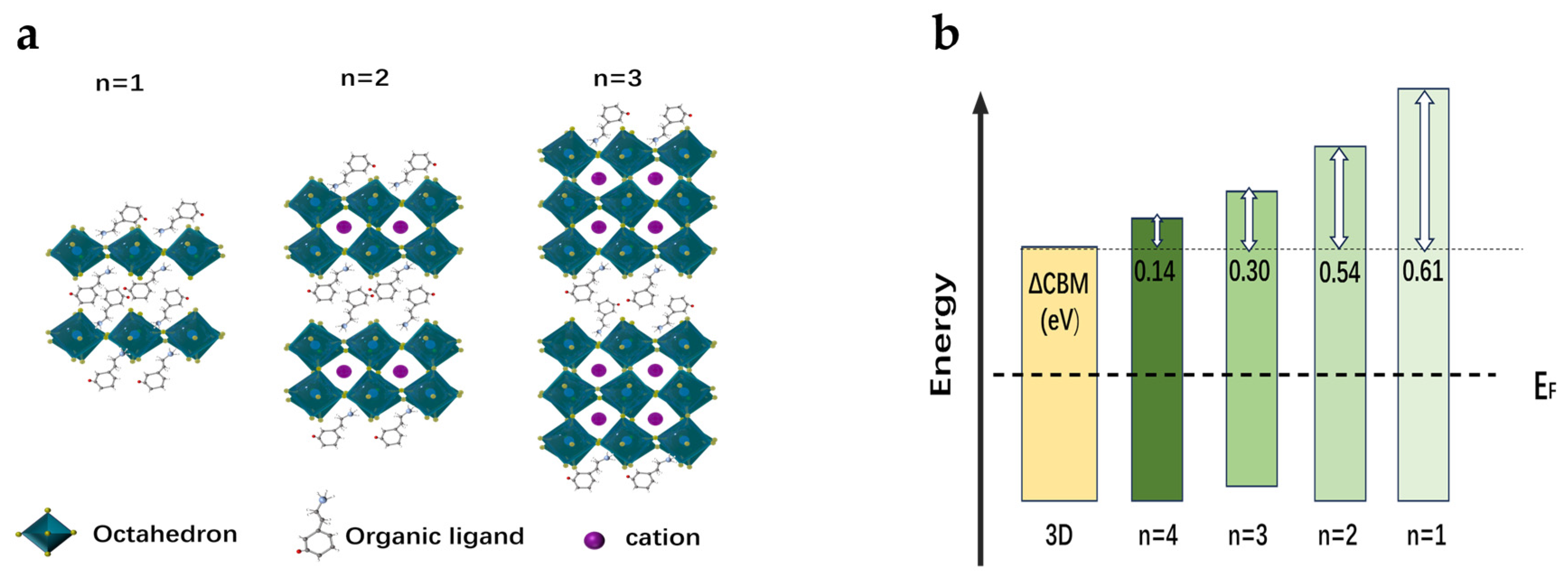
In terms of previously reported work, many well-performing photodiodes used a 2D/3D heterostructure, fabricated via spin coating organic salts onto the surface of 3D perovskites [36]. It was found that this heterostructure boosted performance via enhanced electron blocking. It was beneficial for the negative-intrinsic-positive (NIP) device architecture, in which the 2D-treated perovskite surface was coated with an EBL. However, in this work, such strategy can hinder carrier transport, because 2D-treated perovskite surface was coated with an ETL. It is worth noting that 2D perovskites are perovskite quantum well layers confined between large organic ligands [48]. The number of stacked lead (Pb) octahedra between the organic spacers determines the width of the 2D layer: n = 1, 2, 3 and so on, as exhibited in Figure 3a. As reported, the CBM of 2D perovskite moves down as the increase of n while the valence band maximum (VBM) is almost unchanged (Figure 3b) [38]. To passivate surface defects and reduce resistance to carrier transport, it is rational to deduce that a capping layer of n ≥ 3 2D perovskites would be beneficial for PIN photodiode performance due to their deeper CBM. As reported, the width of the 2D layer can be modulated by changing the ratio of the 2D ligands to the 3D perovskite precursors in solution [49]. Thereupon, MAI and DMF were introduced to precursor solutions to produce 2D perovskite capping layers containing n ≥ 3 layers. MAI was used to reduce the ratio of 2D ligands to A-site cation and DMF introduced Pb of 3D perovskite surface to 2D perovskite layer [38]. This precursor solution was spin-coated onto the 3D perovskite film, forming the 2D/3D hybrid-dimensional perovskite heterojunctions. In this way, it was thus expected that the passivated perovskite photodiodes can achieve a good trade-off between defect passivation and carrier transport.
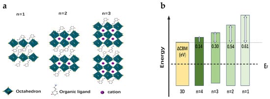
Figure 3.
(a) Schematic of n = 1, 2 and 3 2D structures based on lead iodine perovskite. (b) Band alignment of 3D and 2D perovskites films with different n values.
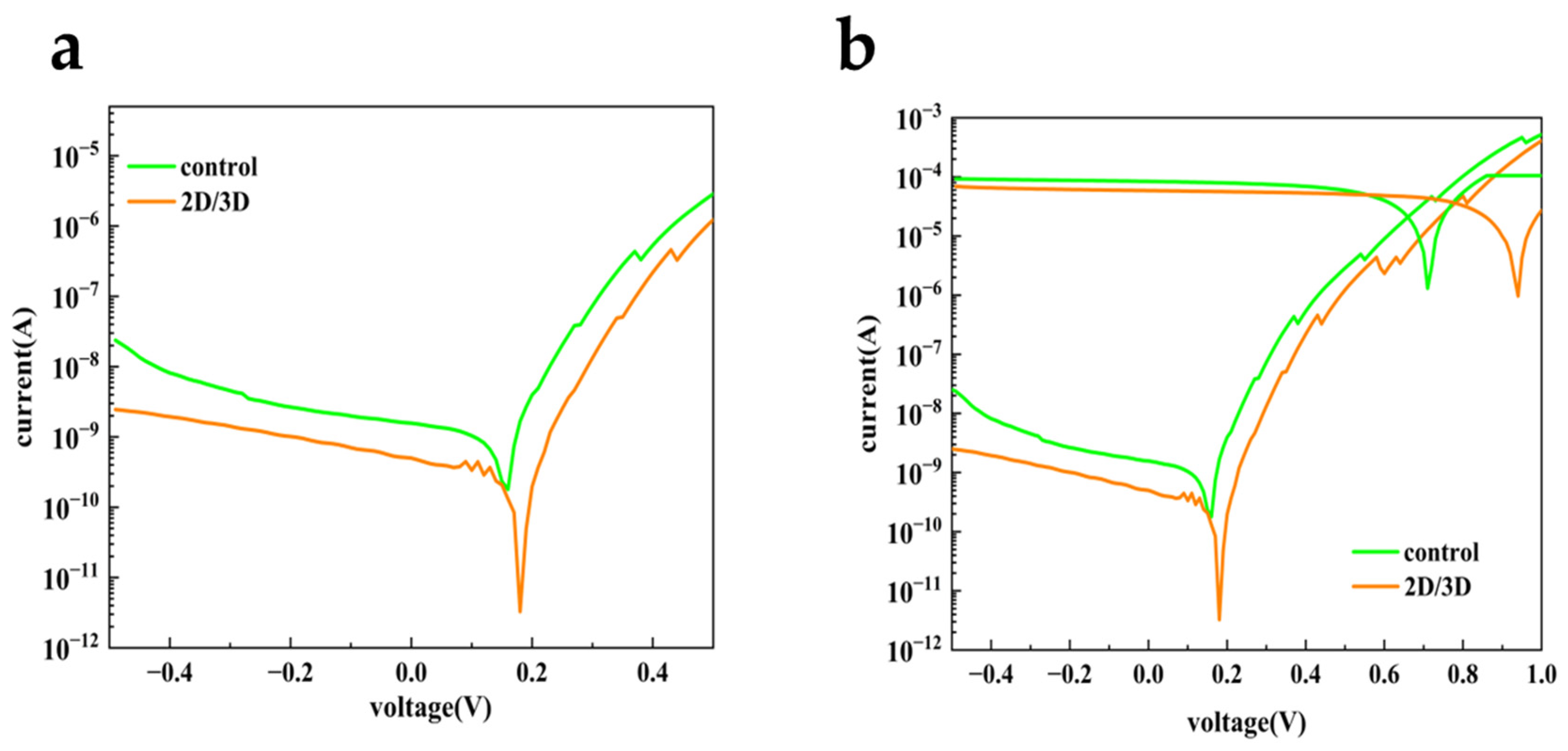
To systematically investigate the impact of 2D/3D hybrid-dimensional perovskite heterojunctions on photodetection capability, the photodiode incorporating this structure and the control device were studied below, respectively. Figure 4a shows the I–V characteristics of perovskite photodiodes in the dark for voltages ranging from −0.5 V to 0.5 V before and after passivation, respectively. It is worth noting that photodiodes after passivation (with 2D/3D heterojunctions) showed much smaller Idark under reverse bias. As illustrated, the minimum value down to 3.2 × 10⁻¹² A of the Idark for the photodiodes with 2D/3D heterojunctions was obtained at 0.18 V, which was two orders of magnitude smaller than that of the control one. The reduced Idark allows the passivated device to detect very weak light, contributing to photodetection sensitivity and signal to noise ratio (SNR). It was reported that the surface defects caused by iodine vacancies mainly contribute to the Idark in the perovskite photodiodes [19]. Together with the former AFM and PL results shown in Figure 1, it can be reasonably deduced that the 2D capping layers successfully passivated the surface defects and suppressed the generation-recombination current density in the dark according to the Shockley–Read–Hall mechanisms. In terms of the non-zero Idark at 0 V bias, this might be associated with different rates of carrier injection from the electrodes, leading to accumulation of excess carriers. Meanwhile, the capacitance increased with accumulation of excess carriers, which could result in the non-zero Idark at 0 V bias [50].
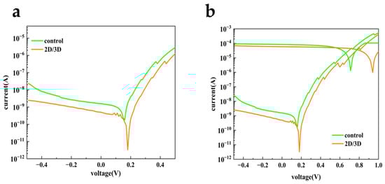
Figure 4.
(a) Idark versus applied voltages for the control perovskite photodiode and the passivated perovskite photodiode; (b) I–V characteristics in the dark and under illumination of 800 nm light for the control and the passivated perovskite photodiodes, respectively.
In addition, to inspect the near-infrared detection performance of the photodiodes, photocurrent curves of the perovskite photodiodes under illumination of 800 nm light are shown in Figure 4b. It can be seen that both devices show excellent photoresponse, while the passivated one maintained the almost identical photocurrent with smaller Idark and larger open circuit voltage (VOC). Namely, the device with 2D/3D heterojunctions was able to deliver more sensitive near-infrared photodetection, lower power consumption and more prominent self-powered work mode. Moreover, the photoresponse behavior also indicated that the resistance to carrier transport of 2D perovskites was reduced due to n ≥ 3 of the 2D capping layer. Usually, the quantum confinement effect would upshift the CBM of the 2D perovskites, resulting in the electron blocking between the 3D perovskite and the EHL. Nevertheless, in this work the electron blocking can be ignored because of the introduction of n ≥ 3 2D perovskites, whose CBM was very close to that of the 3D perovskites.
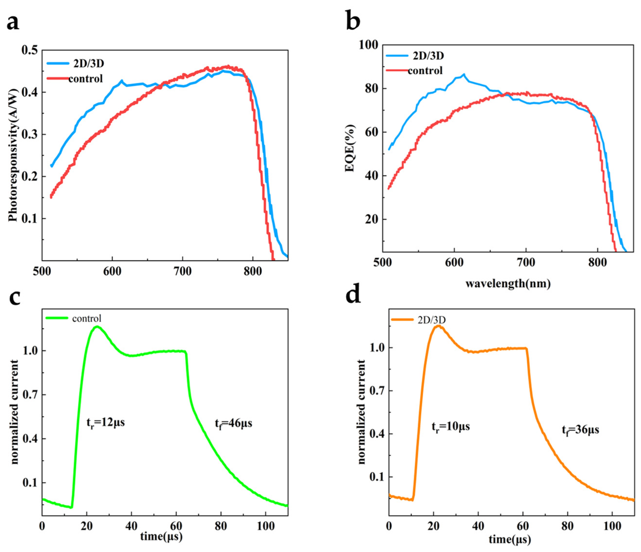
To further demonstrate photodetection performance, Figure 5a shows the wavelength-dependent responsivity of the control and passivated devices working with the self-powered mode, measured at zero bias. The passivated device showed high photoresponsivity over the visible-near-infrared broadband region (500 nm–800 nm), and its cut-off wavelength was ~820 nm. As can be seen, the photoresponsivity of the passivated device was enhanced, but it decreased slightly in the wavelength range of 670 nm~790 nm, which may be due to the electron blocking of the n = 2 2D perovskite [38]. Although this partial decrease of photoresponsivity was existed in the specific range, the D* value of the passivated device would still be larger than that of the control one, because of the obviously restrained Idark. Notably, the champion photoresponsivity value of 0.45 A W−1 was achieved at 760 nm for passivated device. The external quantum efficiency (EQE) is another important parameter for photodetectors, which can be estimated by the following equation:
where h is the Planck’s constant, c is the light speed, and e is the electron charge [6]. As illustrated in Figure 5b, the 2D/3D device delivers a maximum EQE up to 86.6% at zero bias, while the maximum EQE of the control one was 78.4%. Assuming that shot noise from the Idark is the major contributor to the total noise, the D* can be estimated by the following equation:
where A is the active area of the device and R is the photoresponsivity. When under 760 nm illumination, the passivated photodiodes achieved the highest D* of 2.4 × 10¹² Jones due to the low Idark. Additionally, photoresponse speed of the devices under 0 V is evaluated in Figure 5c and 5d, respectively. As illustrated, the passivated photodiode exhibited faster response with rise time of 10 μs and fall time of 36 μs, compared to rise time of 12 μs and fall time of 46 μs for the control photodiode. This difference can be attributed to weak electron blocking between 3D perovskite and 2D capping layers. In addition, the defects on the surface of 3D perovskite can also cause trapping and detrapping processes, resulting in slow response speed in photodiodes. Thus, reduced response time further indicated that the 2D layers effectively passivated the defects and accelerated the photocarrier collection process.
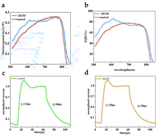
Figure 5.
(a) Photoresponsivity spectra of the control and the passivated photodiodes; (b) The EQE spectra of the control and the passivated photodiodes; (c,d) normalized transient photocurrent response at 0 V for the control and the passivated perovskite photodiodes, respectively.
4. Conclusions
In summary, the passivated perovskite photodiodes with 2D/3D hybrid-dimensional heterojunctions were fabricated, showing high-detectivity, broadband photodetection and the self-powered mode. Significantly, using the 3F-PEAI surface treatment, the 2D perovskite thin layer was formed on the surface of its 3D bulk. In addition, the 2D perovskite capping layers contained n ≥ 3 layers, possessing closer CBM to 3D perovskites and weak electron blocking between 3D perovskites and the ETL. Notably, the surface iodine-vacancy-induced defects were effectively passivated by the 2D perovskites. Consequently, the perovskite photodiodes after passivation exhibited a minimum Idark down to 3.2 × 10⁻¹² A at 0.18 V, a high peak photoresponsivity of 0.45 A W−1 at zero bias and 760 nm light illumination, a high peak D* up to 2.4 × 10¹² Jones and rapid rise/fall time of 10/36 µs. Moreover, the passivated photodiodes were expected to have better environmental stability because of the moisture resistance of 2D perovskites. This study establishes a defect engineering approach through targeted passivation of surface iodine vacancies in metal halide perovskites, which effectively suppresses trap states, optimizes surface/interface charge transport and helps to improve perovskite photodetection sensitivity.
Author Contributions
X.H., H.X. and J.Z. conceived the research idea. X.H. and J.C. prepared samples and performed measurements. G.G. and J.L. drew the diagrams. X.H. wrote the draft manuscript with input from Q.L., H.X. and S.M.W. All the authors contributed to the revision of the final manuscript. All authors have read and agreed to the published version of the manuscript.
Funding
This work was supported by the Haiju Project of Sichuan Province Science and Technology Plan (No. 2024JDHJ0007), the Natural Science Foundation of Sichuan Province under Grant (No. 2022NSFSC0516), the Natural Science and Technology Foundation of Huzhou (No. 2024YZ36).
Institutional Review Board Statement
Not applicable.
Informed Consent Statement
Not applicable.
Data Availability Statement
The data that support the findings of this study are available from the corresponding author upon reasonable request.
Conflicts of Interest
The authors declare no conflicts of interest.
References
- McMeekin, D.P.; Holzhey, P.; Fürer, S.O.; Harvey, S.P.; Schelhas, L.T.; Ball, J.M.; Mahesh, S.; Seo, S.; Hawkins, N.; Lu, J.; et al. Intermediate-Phase Engineering via Dimethylammonium Cation Additive for Stable Perovskite Solar Cells. Nat. Mater. 2023, 22, 73–83. [Google Scholar] [CrossRef] [PubMed]
- Park, J.; Kim, J.; Yun, H.-S.; Paik, M.J.; Noh, E.; Mun, H.J.; Kim, M.G.; Shin, T.J.; Seok, S.I. Controlled Growth of Perovskite Layers with Volatile Alkylammonium Chlorides. Nature 2023, 616, 724–730. [Google Scholar] [CrossRef] [PubMed]
- Yang, S.J.; Wang, K.; Luo, Y.; Park, J.Y.; Yang, H.; Coffey, A.H.; Ma, K.; Sun, J.; Wieghold, S.; Zhu, C.; et al. Two-Factor Phase Separations in Mixed-Halide Quasi-2D Perovskite LEDs: Dimensionality and Halide Segregations. ACS Energy Lett. 2023, 8, 3693–3701. [Google Scholar] [CrossRef]
- Liu, Y.; Wang, S.; Yu, Z.; Chen, G.; Wang, C.; Wang, T.; Ke, W.; Fang, G. A Multifunctional Additive Strategy Enables Efficient Pure-Blue Perovskite Light-Emitting Diodes. Adv. Mater. 2023, 35, 2302161. [Google Scholar] [CrossRef]
- Zhan, Z.; Lin, D.; Cai, J.; Lu, Y.; Chen, A.; Zhang, T.; Chen, K.; Liu, P.; Wang, X.; Xie, W. A Perovskite Photodetector Crossbar Array by Vapor Deposition for Dynamic Imaging. Adv. Mater. 2022, 34, 2207106. [Google Scholar] [CrossRef] [PubMed]
- Wang, H.; Kim, D.H. Perovskite-Based Photodetectors: Materials and Devices. Chem. Soc. Rev. 2017, 46, 5204–5236. [Google Scholar] [CrossRef]
- Najarian, A.M.; Vafaie, M.; Johnston, A.; Zhu, T.; Wei, M.; Saidaminov, M.I.; Hou, Y.; Hoogland, S.; De Arquer, F.P.G.; Sargent, E.H. Sub-Millimetre Light Detection and Ranging Using Perovskites. Nat. Electron. 2022, 5, 511–518. [Google Scholar] [CrossRef]
- Herz, L.M. Charge-Carrier Mobilities in Metal Halide Perovskites: Fundamental Mechanisms and Limits. ACS Energy Lett. 2017, 2, 1539–1548. [Google Scholar] [CrossRef]
- Stranks, S.D.; Eperon, G.E.; Grancini, G.; Menelaou, C.; Alcocer, M.J.P.; Leijtens, T.; Herz, L.M.; Petrozza, A.; Snaith, H.J. Electron-Hole Diffusion Lengths Exceeding 1 Micrometer in an Organometal Trihalide Perovskite Absorber. Science 2013, 342, 341–344. [Google Scholar] [CrossRef]
- Kim, T.; Jeong, S.; Kim, K.-H.; Shim, H.; Kim, D.; Kim, H.-J. Engineered Surface Halide Defects by Two-Dimensional Perovskite Passivation for Deformable Intelligent Photodetectors. ACS Appl. Mater. Interfaces 2022, 14, 26004–26013. [Google Scholar] [CrossRef]
- Chen, C.-W.; Hsiao, S.-Y.; Chen, C.-Y.; Kang, H.-W.; Huang, Z.-Y.; Lin, H.-W. Optical Properties of Organometal Halide Perovskite Thin Films and General Device Structure Design Rules for Perovskite Single and Tandem Solar Cells. J. Mater. Chem. A 2015, 3, 9152–9159. [Google Scholar] [CrossRef]
- Shen, K.; Xu, H.; Li, X.; Guo, J.; Sathasivam, S.; Wang, M.; Ren, A.; Choy, K.L.; Parkin, I.P.; Guo, Z.; et al. Flexible and Self-Powered Photodetector Arrays Based on All-Inorganic CsPbBr3 Quantum Dots. Adv. Mater. 2020, 32, 2000004. [Google Scholar] [CrossRef]
- Yao, J.; Zhou, Z.; Li, L.; Chen, Y.; Wang, C.; Wang, X.; Lu, Z.; Bai, Z.; Zhang, Q.; Huangfu, X.; et al. Zero-Dimensional Cs3BiX6 (X = Br, Cl) Single Crystal Films with Second Harmonic Generation. Nanoscale Res. Lett. 2022, 17, 115. [Google Scholar] [CrossRef] [PubMed]
- Fang, Y.; Dong, Q.; Shao, Y.; Yuan, Y.; Huang, J. Highly Narrowband Perovskite Single-Crystal Photodetectors Enabled by Surface-Charge Recombination. Nat. Photon. 2015, 9, 679–686. [Google Scholar] [CrossRef]
- Dou, L.; Yang, Y.; You, J.; Hong, Z.; Chang, W.-H.; Li, G.; Yang, Y. Solution-Processed Hybrid Perovskite Photodetectors with High Detectivity. Nat. Commun. 2014, 5, 5404. [Google Scholar] [CrossRef]
- Kublitski, J.; Hofacker, A.; Boroujeni, B.K.; Benduhn, J.; Nikolis, V.C.; Kaiser, C.; Spoltore, D.; Kleemann, H.; Fischer, A.; Ellinger, F.; et al. Reverse Dark Current in Organic Photodetectors and the Major Role of Traps as Source of Noise. Nat. Commun. 2021, 12, 551. [Google Scholar] [CrossRef]
- Li, Y.; Li, Q.; Wang, Z.; Huang, Z.; Zhu, J.; Channa, A.I.; Cui, F.; Xu, H.; Li, X.; Zhou, L.; et al. High External Quantum Efficiency Monolayer MoS2(1−x)Se2x Phototransistor with Alloying-Induced near-Infrared Absorption. Appl. Phys. Lett. 2023, 123, 151103. [Google Scholar] [CrossRef]
- Na, W.; Zhang, J.; Cui, F.; Li, X.; Shen, K.; Wu, J.; Zou, G.; Xu, H. Novel 2D Glassy-Graphene for Photodetection and Sensing. In Proceedings of the 2024 24th International Conference on Transparent Optical Networks (ICTON), Bari, Italy, 14–18 July 2024; IEEE: New York, NY, USA; pp. 1–5. [Google Scholar]
- Yin, Z.; Chen, Y.; Zhang, Y.; Yuan, Y.; Yang, Q.; Zhong, Y.; Gao, X.; Xiao, J.; Wang, Z.; Xu, J.; et al. Probing into Reverse Bias Dark Current in Perovskite Photodiodes: Critical Role of Surface Defects. Adv. Funct. Mater. 2023, 33, 2302199. [Google Scholar] [CrossRef]
- Shen, L.; Fang, Y.; Wang, D.; Bai, Y.; Deng, Y.; Wang, M.; Lu, Y.; Huang, J. A Self-Powered, Sub-Nanosecond-Response Solution-Processed Hybrid Perovskite Photodetector for Time-Resolved Photoluminescence-Lifetime Detection. Adv. Mater. 2016, 28, 10794–10800. [Google Scholar] [CrossRef]
- Ahmadi, M.; Wu, T.; Hu, B. A Review on Organic–Inorganic Halide Perovskite Photodetectors: Device Engineering and Fundamental Physics. Adv. Mater. 2017, 29, 1605242. [Google Scholar] [CrossRef]
- Shi, D.; Adinolfi, V.; Comin, R.; Yuan, M.; Alarousu, E.; Buin, A.; Chen, Y.; Hoogland, S.; Rothenberger, A.; Katsiev, K.; et al. Low Trap-State Density and Long Carrier Diffusion in Organolead Trihalide Perovskite Single Crystals. Science 2015, 347, 519–522. [Google Scholar] [CrossRef] [PubMed]
- Fang, Y.; Huang, J. Resolving Weak Light of Sub-picowatt per Square Centimeter by Hybrid Perovskite Photodetectors Enabled by Noise Reduction. Adv. Mater. 2015, 27, 2804–2810. [Google Scholar] [CrossRef] [PubMed]
- Ollearo, R.; Wang, J.; Dyson, M.J.; Weijtens, C.H.L.; Fattori, M.; Van Gorkom, B.T.; Van Breemen, A.J.J.M.; Meskers, S.C.J.; Janssen, R.A.J.; Gelinck, G.H. Ultralow Dark Current in Near-Infrared Perovskite Photodiodes by Reducing Charge Injection and Interfacial Charge Generation. Nat. Commun. 2021, 12, 7277. [Google Scholar] [CrossRef]
- Wang, M.; Cao, F.; Wang, M.; Deng, K.; Li, L. Intermediate-Adduct-Assisted Growth of Stable CsPbI2 Br Inorganic Perovskite Films for High-Efficiency Semitransparent Solar Cells. Adv. Mater. 2021, 33, 2006745. [Google Scholar] [CrossRef] [PubMed]
- Tabi, G.D.; Pham, H.T.; Zhan, H.; Walter, D.; Mayon, A.O.; Peng, J.; Duong, T.; Shehata, M.M.; Shen, H.; Duan, L.; et al. LiI Doping of Mixed-Cation Mixed-Halide Perovskite Solar Cells: Defect Passivation, Controlled Crystallization and Transient Ionic Response. Mater. Today Phys. 2022, 27, 100822. [Google Scholar] [CrossRef]
- Byranvand, M.M.; Kodalle, T.; Zuo, W.; Friedlmeier, T.M.; Abdelsamie, M.; Hong, K.; Zia, W.; Perween, S.; Clemens, O.; Sutter-Fella, C.M.; et al. One-Step Thermal Gradient- and Antisolvent-Free Crystallization of All-Inorganic Perovskites for Highly Efficient and Thermally Stable Solar Cells. Adv. Sci. 2022, 9, 2202441. [Google Scholar] [CrossRef]
- Zhao, Y.; Li, C.; Jiang, J.; Wang, B.; Shen, L. Sensitive and Stable Tin–Lead Hybrid Perovskite Photodetectors Enabled by Double-Sided Surface Passivation for Infrared Upconversion Detection. Small 2020, 16, 2001534. [Google Scholar] [CrossRef]
- Zhao, Y.; Jiao, S.; Liu, S.; Jin, Y.; Yang, S.; Wang, X.; Liu, T.; Jin, H.; Wang, D.; Gao, S.; et al. Surface Passivation of CsPbBr3 Films by Interface Engineering in Efficient and Stable Self-Powered Perovskite Photodetector. J. Alloy. Compd. 2023, 965, 171434. [Google Scholar] [CrossRef]
- Jiang, Q.; Zhao, Y.; Zhang, X.; Yang, X.; Chen, Y.; Chu, Z.; Ye, Q.; Li, X.; Yin, Z.; You, J. Surface Passivation of Perovskite Film for Efficient Solar Cells. Nat. Photon. 2019, 13, 460–466. [Google Scholar] [CrossRef]
- Sun, Z.; Amrillah, T. Potential Application of Bismuth Oxyiodide (BiOI) When It Meets Light. Nanoscale 2024, 16, 5079–5106. [Google Scholar] [CrossRef]
- Cao, F.; Zhang, P.; Li, L. Multidimensional Perovskite Solar Cells. Fundam. Res. 2022, 2, 237–253. [Google Scholar] [CrossRef] [PubMed]
- Cheng, W.; Wu, S.; Lu, J.; Li, G.; Li, S.; Tian, W.; Li, L. Self-Powered Wide-Narrow Bandgap-Laminated Perovskite Photodetector with Bipolar Photoresponse for Secure Optical Communication. Adv. Mater. 2024, 36, 2307534. [Google Scholar] [CrossRef] [PubMed]
- Metcalf, I.; Sidhik, S.; Zhang, H.; Agrawal, A.; Persaud, J.; Hou, J.; Even, J.; Mohite, A.D. Synergy of 3D and 2D Perovskites for Durable, Efficient Solar Cells and Beyond. Chem. Rev. 2023, 123, 9565–9652. [Google Scholar] [CrossRef]
- Chen, R.; Shen, L.; Zheng, L.; Zhu, T.; Liu, Y.; Liu, L.; Zheng, J.; Gong, X. Two-/Three-Dimensional Perovskite Bilayer Thin Films Post-Treated with Solvent Vapor for High-Performance Perovskite Photovoltaics. ACS Appl. Mater. Interfaces 2021, 13, 49104–49113. [Google Scholar] [CrossRef] [PubMed]
- Lai, L.; Liu, G.; Zhou, Y.; He, X.; Ma, Y. Modulating Dimensionality of 2D Perovskite Layers for Efficient and Stable 2D/3D Perovskite Photodetectors. ACS Appl. Mater. Interfaces 2024, 16, 19849–19857. [Google Scholar] [CrossRef]
- Li, H.; Zhang, C.; Gong, C.; Zhang, D.; Zhang, H.; Zhuang, Q.; Yu, X.; Gong, S.; Chen, X.; Yang, J.; et al. 2D/3D Heterojunction Engineering at the Buried Interface towards High-Performance Inverted Methylammonium-Free Perovskite Solar Cells. Nat. Energy 2023, 8, 946–955. [Google Scholar] [CrossRef]
- Chen, H.; Teale, S.; Chen, B.; Hou, Y.; Grater, L.; Zhu, T.; Bertens, K.; Park, S.M.; Atapattu, H.R.; Gao, Y.; et al. Quantum-Size-Tuned Heterostructures Enable Efficient and Stable Inverted Perovskite Solar Cells. Nat. Photon. 2022, 16, 352–358. [Google Scholar] [CrossRef]
- Zhou, Q.; Gao, Y.; Cai, C.; Zhang, Z.; Xu, J.; Yuan, Z.; Gao, P. Dually-Passivated Perovskite Solar Cells with Reduced Voltage Loss and Increased Super Oxide Resistance. Angew. Chem. 2021, 133, 8384–8393. [Google Scholar] [CrossRef]
- Wang, X.; Rakstys, K.; Jack, K.; Jin, H.; Lai, J.; Li, H.; Ranasinghe, C.S.K.; Saghaei, J.; Zhang, G.; Burn, P.L.; et al. Engineering Fluorinated-Cation Containing Inverted Perovskite Solar Cells with an Efficiency of >21% and Improved Stability towards Humidity. Nat. Commun. 2021, 12, 52. [Google Scholar] [CrossRef]
- Zhu, H.; Ren, Y.; Pan, L.; Ouellette, O.; Eickemeyer, F.T.; Wu, Y.; Li, X.; Wang, S.; Liu, H.; Dong, X.; et al. Synergistic Effect of Fluorinated Passivator and Hole Transport Dopant Enables Stable Perovskite Solar Cells with an Efficiency Near 24%. J. Am. Chem. Soc. 2021, 143, 3231–3237. [Google Scholar] [CrossRef]
- Qiu, Y.; Liang, J.; Zhang, Z.; Deng, Z.; Xu, H.; He, M.; Wang, J.; Yang, Y.; Kong, L.; Chen, C.-C. Tuning the Interfacial Dipole Moment of Spacer Cations for Charge Extraction in Efficient and Ultrastable Perovskite Solar Cells. J. Phys. Chem. C 2021, 125, 1256–1268. [Google Scholar] [CrossRef]
- Azmi, R.; Ugur, E.; Seitkhan, A.; Aljamaan, F.; Subbiah, A.S.; Liu, J.; Harrison, G.T.; Nugraha, M.I.; Eswaran, M.K.; Babics, M.; et al. Damp Heat–Stable Perovskite Solar Cells with Tailored-Dimensionality 2D/3D Heterojunctions. Science 2022, 376, 73–77. [Google Scholar] [CrossRef]
- Lin, Y.-H.; Sakai, N.; Da, P.; Wu, J.; Sansom, H.C.; Ramadan, A.J.; Mahesh, S.; Liu, J.; Oliver, R.D.J.; Lim, J.; et al. A Piperidinium Salt Stabilizes Efficient Metal-Halide Perovskite Solar Cells. Science 2020, 369, 96–102. [Google Scholar] [CrossRef] [PubMed]
- Chen, S.; Xiao, X.; Gu, H.; Huang, J. Iodine Reduction for Reproducible and High-Performance Perovskite Solar Cells and Modules. Sci. Adv. 2021, 7, eabe8130. [Google Scholar] [CrossRef] [PubMed]
- Zheng, X.; Hou, Y.; Bao, C.; Yin, J.; Yuan, F.; Huang, Z.; Song, K.; Liu, J.; Troughton, J.; Gasparini, N.; et al. Managing Grains and Interfaces via Ligand Anchoring Enables 22.3%-Efficiency Inverted Perovskite Solar Cells. Nat. Energy 2020, 5, 131–140. [Google Scholar] [CrossRef]
- Bai, S.; Da, P.; Li, C.; Wang, Z.; Yuan, Z.; Fu, F.; Kawecki, M.; Liu, X.; Sakai, N.; Wang, J.T.-W.; et al. Planar Perovskite Solar Cells with Long-Term Stability Using Ionic Liquid Additives. Nature 2019, 571, 245–250. [Google Scholar] [CrossRef]
- Blancon, J.-C.; Even, J.; Stoumpos, C.C.; Kanatzidis, M.G.; Mohite, A.D. Semiconductor Physics of Organic–Inorganic 2D Halide Perovskites. Nat. Nanotechnol. 2020, 15, 969–985. [Google Scholar] [CrossRef]
- Quan, L.N.; Yuan, M.; Comin, R.; Voznyy, O.; Beauregard, E.M.; Hoogland, S.; Buin, A.; Kirmani, A.R.; Zhao, K.; Amassian, A.; et al. Ligand-Stabilized Reduced-Dimensionality Perovskites. J. Am. Chem. Soc. 2016, 138, 2649–2655. [Google Scholar] [CrossRef]
- Zhao, Z.; Wang, J.; Xu, C.; Yang, K.; Zhao, F.; Wang, K.; Zhang, X.; Zhang, F. Photomultiplication Type Broad Response Organic Photodetectors with One Absorber Layer and One Multiplication Layer. J. Phys. Chem. Lett. 2020, 11, 366–373. [Google Scholar] [CrossRef]

Disclaimer/Publisher’s Note: The statements, opinions and data contained in all publications are solely those of the individual author(s) and contributor(s) and not of MDPI and/or the editor(s). MDPI and/or the editor(s) disclaim responsibility for any injury to people or property resulting from any ideas, methods, instructions or products referred to in the content. |
© 2025 by the authors. Licensee MDPI, Basel, Switzerland. This article is an open access article distributed under the terms and conditions of the Creative Commons Attribution (CC BY) license (https://creativecommons.org/licenses/by/4.0/).