Abstract
The passivation engineering of the hole transport layer in perovskite solar cells (PSCs) has significantly decreased carrier accumulation and open circuit voltage (Voc) loss, as well as energy band mismatching, thus achieving the goal of high-power conversion efficiency. However, most devices incorporating organic/inorganic buffer layers suffer from poor stability and low efficiency. In this article, we have proposed an inorganic buffer layer of Cu2O, which has achieved high efficiency on lower work function metals and various frequently used hole transport layers (HTLs). Once the Cu2O buffer layer was applied to modify the Cu/PTAA interface, the device exhibited a high Voc of 1.20 V, a high FF of 75.92%, and an enhanced PCE of 22.49% versus a Voc of 1.12 V, FF of 69.16%, and PCE of 18.99% from the (PTAA/Cu) n-i-p structure. Our simulation showed that the application of a Cu2O buffer layer improved the interfacial contact and energy alignment, promoting the carrier transportation and reducing the charge accumulation. Furthermore, we optimized the combinations of the thicknesses of the Cu2O, the absorber layer, and PTAA to obtain the best performance for Cu-based perovskite solar cells. Eventually, we explored the effect of the defect density between the HTL/absorber interface and the absorber/ETL interface on the device and recommended the appropriate reference defect density for experimental research. This work provides guidance for improving the experimental efficiency and reducing the cost of perovskite solar cells.
1. Introduction
Organic-inorganic perovskite solar cells (PSCs) have exhibited an exciting tendency, with high performance from 3.8% to nearly 26.0% in power conversion efficiency (PCE) [1], motivating great research interest in the field of photovoltaics. Although PSCs can achieve higher energy conversion efficiency, there is a long way to go regarding its theoretical limitation of PCE. One apparent reason is the charge accumulation between the metal electrode and functional layers. With the charge accumulated at the interface, the energy level mismatch and potential barrier effect were enhanced because of the reversed electric-field attached by the charge accumulation. Therefore, optimizing interfacial contact and improving interfacial energy level alignment is an important way to reduce charge accumulation and promote hole extraction, which has drawn the attention of the scientific community regarding PSCs.
The performance of an optoelectronic device critically depends on the transport ability of carriers between interfaces inside of PSCs. Charge accumulation or recombination would occur if the charge carriers encounter a higher barrier or a high interface-state density [2]. To address this problem, buffer layers have frequently been used to enhance carrier injection, decrease trap-states, and decrease contact resistance in various solar cells [2]. Specifically, the buffer layer between the hole transport layer (HTL) and the anode has a main function of blocking the migration of electrons towards the metal electrode, reducing interfacial recombination, and promoting hole transportation [3]. Several attempts have been made to modify the HTL/electrode in PSCs using organic interlayers to improve the interface and interlayer properties to overcome the interface loss. For instance, Arora et al. concluded that the instability of PSCs mainly originates from the CuSCN/Au interface contact and is not related to the degradation of the CuSCN/perovskite interface, so they introduced a thin conductive rGO (reduced graphene oxide) modified layer between CuSCN and Au to effectively alleviate the problem of interface degradation [4]. Zhou et al. introduced a poly-TPD ultra-thin layer to modify the HTL/Ag interface, thereby improving the efficiency of the solar cell (from 5.95% to 10.36%) because it can smooth the barrier between the HTL and electrode to promote the transmission of holes and passivate the surface defects to improve the interface contact [5]. However, for organic materials, the stability is a deadly point when they are employed in a complex environment. Therefore, researchers are exploiting transition metal oxides (TMOs) as interfacial buffer layers for extracting photogenerated holes; the metal oxides were demonstrated to exhibit good processability, transparency, and charge transport properties, as well as excellent stability [6]. Cai et al. found that the addition of NiO nanoparticles (as both the HTL and buffer layer) between the perovskite film and the carbon electrode can effectively promote the separation and extraction of photogenerated carriers and inhibit the charge recombination at the perovskite layer/carbon electrode interface, and they achieved the highest efficiency of 13.6% [7]. Zhao et al. demonstrated that the efficiency (11.4%) of a perovskite solar cell obtained by adding MoOx between the HTL and Al electrode is comparable to that of a cell using a standard Ag top electrode, which is due to the effectiveness of the hole extraction using MoOx [8]. On the downside, NiOx is often grown by sputtering, which may destroy the organic charge transport and perovskite layer [9]. MoOx reacts strongly with the lead halide perovskite, hampering its long-term stability [10,11]. Nevertheless, NiO and MoOx both show obvious disadvantages that limit the improvement of their efficiency because of their lower hole mobility of about 1.6 × 10⁻⁴–1.6 × 10⁻³ cm2/(V·s) and 7.8 cm2/(V·s), respectively [3]; thus, there is still significant room for exploration concerning HTL/electrode interface optimization. Overall, these issues continue to motivate further research to explore efficient buffer layers with relative stability and good interfacial contact. A recent theoretical study proposed that Cu2O might outperform other TMOs [12]. Moreover, Cu2O has been studied for decades as a typical p-type semiconductor due to its unique physical properties and applications in areas ranging from photo electrochemistry to magneto electrics and superconductors [13]. Apart from its natural p-type conductivity, Cu2O also possesses a high carrier mobility of over 100 cm2/(V·s) and a long carrier diffusion length ranging up to several micrometers [14]. Moreover, Cu2O can be grown at temperatures below 200 °C through soft growth methods using chemical vapor deposition (CVD) or atomic layer deposition (ALD) [15]. The unique characteristics of Cu2O make it a promising candidate for solar cell applications, and rare investigations have been carried out using Cu2O as a buffer layer to modify the HTL/electrode interface.
Thus, in this paper, we reported Cu2O as buffer between metal electrode/hole transport materials (HTMs) based on using a solar cell capacitance simulator (SCAPS-1D) to help understand the beneficial effect of Cu2O on device performance. The basic model structure of PSC we built is: metal electrode/Cu2O (with/without buffer layer)/HTL (multiple hole transport materials in model)/MAPbI3(perovskite absorber layer)/SnO2 (electron transport layer)/FTO (transparent conductive oxide). Initially, we employed Spiro-OMeTAD as the HTM and investigated the effect of Cu2O on different metal electrodes and found that Cu2O can effectively improve the performance of Cu-based devices. Then we compared the performance of the device, with and without a Cu2O buffer layer, based on a Cu electrode to vary different HTM, and the results showed that the device with PTAA-HTL showed the most enhanced performance (without Cu2O—PCE:18.99%, with Cu2O—PCE: 22.49%). Finally, we explained the optimization of the thickness combinations of the buffer layer for achieving the highest PCE.
2. Device Structure and Simulation Parameters
In this work, we use the key platform SCAPS-1D to simulate the MAPbI3-based heterojunction perovskite solar cells. The software SCAPS (version 3.3.10) is a superb and powerful tool for helping us to clearly understand the physical behavior of the different optoelectronic properties of any solar cell [16]. The principle of SCAPS software is based mainly on two basic equations: the Poisson equation and the continuity equation of electrons and holes under a steady-state condition.
The Poisson equation can be given by:
where ψ is electrostatic potential, and εr are relative and the vacuum permittivity, e is electrical charge, p and n are hole and electron concentrations, ND and NA are charged impurities of the donor and acceptor type, and ρP and ρN are hole and electron distribution, respectively.
The continuity equations of electrons and holes can be described by:
where Jn and Jp are electron and hole current densities, G is the generation rate, and R is the recombination rate.
In this simulation work, the structure of the solar cell model is: metal electrode/Cu2O (with/without buffer layer)/Spiro-OMeTAD (HTL)/MAPbI3 (perovskite absorber layer)/SnO2 (ETL)/FTO (transparent conductive oxide), as shown in Figure 1. The parameters (thickness, band gap, dielectric permittivity, electron affinity, electron/hole mobility, electron/hole thermal velocity, defect density, etc.) used for the solar cell structure in this simulation are shown in Table 1. Values of the input parameters are taken from the references given in the tables. The parameters of the interface defect layers are given in Table S1. The parameters of the back and front electrodes are given in Table S2 (the work function of FTO set to 4.4 eV). The list of work functions of the back metal electrodes used are given in Table S3.
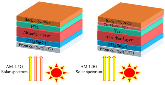
Figure 1.
The n-i-p typical perovskite solar cell structure (left) and the structure with a Cu2O buffer layer (right).

Table 1.
Primary input parameters used for the simulation of perovskite solar cells.
In SCAPS, the data for the absorption coefficient () versus the wavelength () can be imported from an external source; the absorption data used in this paper are taken from the literature, as shown in the Supplementary Information (see Figure S1). The simulation is carried out under the AM 1.5G solar spectrum, with an incident power density of 1000 W/m2 at room temperature (300 K).
3. Result and Discussion
3.1. Reference Device Performance
Solar cell harvest photons and then convert energy to electric energy for output. Generally, the complex energy conversion process can be approximately summarized into three steps: (1) the photon absorption and electron excitation [23], in which the perovskite material absorbs the incident photons with energy greater than its band gap, and is excited to generate excitons; (2) the charge transportation [24], in which the excitons separate and transfer to the hole transport layer and the electron transport layer, respectively; (3) the charge extraction [25], in which the carriers drift to the electrodes and eventually form a current through the external circuit. Note that the recombination process is also an important step not mentioned here. Then, based on the above-mentioned conversion process, the selections of an absorber, transportation material, and electrodes, as well as the structural design, are crucial to PSCs. Methyl lead triiodide (MAPbI3) was applied in the model as the absorber layer because of its high absorption coefficient in the visible range, leading to excellent photoelectronic properties [26]. According to previous research [27], the thickness design was set in the 0.5 to 0.6 µm range for balancing the light absorption and charge extraction. Meanwhile, to simplify the model, we have chosen the most-used SnO2 as the ETL in this article because of its unique advantage in high electron extraction capability compared to other ETLs [28]. After referring to other works relating to SnO2 ETL, we determined that the device shows better performance when the SnO2 thickness is 0.07 µm, which inspired our model [20,29]. Simultaneously, the application of HTL is equally important to the device performance; the selection and the thickness optimization of the HTL are also hot research topics in the scientific community [30,31]. Particularly when using SnO2 as the ETL, most articles have found that the best thickness of the HTLs was around 0.15 µm. Finally, the metal electrode used to extract the charge also has a great influence on the solar performance. Based on the short summary above, MAPI3 perovskite devices based on SnO2 (ETL), Spiro-OMeTAD (HTL), and Ag (electrode) were initially applied in our model to check the simulation accuracy. The PCE of the simulated model was 20.13%, which is in accordance with Zhao’s report [32].
3.2. Effect of Cu2O Buffer Layer on Various Metal Electrodes
It was found that in HTL-free perovskite solar cells, iodide ions and methylamine ions at the grain boundaries easily diffuse and react with the Ag electrode surface, which will degrade the performance of the device [33]. Thus, to improve device stability, there is an urgent need to find materials that can replace Ag electrodes. With the proposed model, we can explore the effect of Cu2O on different metal electrodes by comparing the two cases, with or without the Cu2O buffer layer, to find the metal electrode that best matches Cu2O. Generally, Cr (4.5 eV), Cu (4.65 eV), Ag (4.7 eV), Au (5.1 eV), Ni (5.15 eV), and Pt (5.65 eV) (Table S3) are the most frequently used electrode materials.
First, we clearly observed changes in the Jsc, Voc, FF, and PCE values by changing the work function of the back electrode without adding a Cu2O buffer layer. Jsc was almost unchanged, and Voc showed a brief promotion with a decreasing work function, then remained almost the same for a work function greater than 4.65 eV (work function of Au electrode) (Figure 2a,b). However, for both FF and PCE, the work function increased significantly and then reached a maximum at 5.1 eV (work function of Au electrode) (Figure 2c,d). These conditions are caused by the Schottky barrier between the HTL/electrode, which is inversely proportional to the back electrode work function, and the high energy barrier hinders the carrier transportation. For p-type semiconductors, a good ohmic contact is easily formed with a high metal work function [34]. Therefore, under the typical n-i-p structure, to obtain sufficient photovoltaic performance, it is required to select an expensive metal (such as Au), with a work function higher than 5.1 eV, for the back electrode, which is not conducive to the industrialization of perovskites.
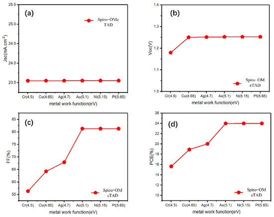
Figure 2.
(a–d) The photovoltaic parameters (Jsc, Voc, FF, PCE) for the reference n-i-p devices with Spiro-OMeTAD-HTL and different electrodes.
After inserting the Cu2O buffer layer between the HTL/electrode, most of the parameters showed an increasing trend at the beginning, maintaining stability after 5.1 eV, and the change of Jsc is only slight (Figure 3). However, by comparing the FF, PCE before and after inserting the Cu2O (Figure 3c,d, it can be clearly seen that the Cu2O buffer layer can effectively improve the FF of Cu electrode devices (from 66.07% to 77.03%), thus improving its PCE (from 18.92% to 21.46%), even for other devices with lower work function electrodes (Cr, Ag), the buffer layer can also have a similar effect. The Schottky barrier will form between the HTL and the low work function metal electrode, and the Schottky contact may lead to the decrease in Voc of the device [35]; this is the reason why the Cu electrode device is not efficient when the Cu2O buffer layer is not added. In similar research, Lin et al. added a CuOx interlayer between the carrier transport layer and Ag or Al and found that the CuOx film, which mainly consists of Cu2O, can effectively reduce the barrier height between this interface, transforming the Schottky contact into an excellent ohmic contact [36]. Moreover, Table 2 shows a photovoltaic parameters table showing different HTL devices, with and without a Cu2O buffer layer, using an Au electrode, and our simulated device results are compared with recently published reports. We can see that for these HTMs with wide bandgap (Table 2), the addition of a Cu2O buffer layer did not change the photovoltaic parameters (Jsc, Voc, FF, PCE) while using an Au electrode device. For the remaining HTMs with a narrow bandgap, the addition of Cu2O only marginally improved the device performance. The few slightly increased PCEs may be attributed to the high hole mobility and wide band gap of Cu2O. Thus, we speculated that the addition of Cu2O can effectively reduce the Schottky barrier between the HTL and Cu, as well as the low work function of the metal, and facilitate hole transportation from the HTL to the electrode. However, for metals such as Au, in which the energy barrier between the high work function electrode is already small, the role of Cu2O in reducing the energy barrier appears to be minimal. Furthermore, according to previous research, the introduction of a trace amount of AgI at the HTL/Ag interface can effectively increase the work function of Ag, which eliminates the downward band bending between the HTL and the Ag electrode [37]. From another point of view, inserting a Cu2O buffer layer between HTL/Cu may increase the work function of the Cu electrode in a disguised form. Nevertheless, for an Au electrode, if the Cu2O also increases its work function, the performance of the device will not increase because all PV parameters have approached the maximum saturation value at 5.1 eV.
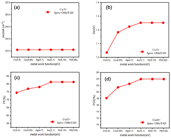
Figure 3.
(a–d) The photovoltaic parameters (Jsc, Voc, FF, PCE) for the Cu2O buffer layer contained devices with Spiro-OMeTAD-HTL and different electrodes.
Table 2.
Photovoltaic parameters obtained using different HTMs by using an Au electrode (with and without Cu2O).
Therefore, inserting a Cu2O buffer between the HTL/electrode interface is an excellent strategy to improve solar cell performance with a Cu electrode. At the same time, J Huang et al. found that Cu metal was stable compared to other metals when MAPbI3 is used as the absorber layer [42]. As a low-cost and stable electrode, the application of Cu is an idea candidate for simulation, as well as further industrialization. In the following section, we will demonstrate the superiority of the Cu2O buffer layer over different HTLs.
3.3. The Effect of a Cu2O Buffer Layer with HTLs
To enhance the performance of perovskite solar cells, the HTL has a crucial impact on the device PCE by transporting holes and suppressing recombination after exciton dissociation [43]. The existing commercial hole transport material Spiro-OMeTAD exhibits disadvantages such as long synthesis cycle, complicated processing, high cost, and low stability, and the photoelectric conversion efficiency (PCE) of PSCs with Spiro-OMeTAD basically reaches the upper limit of 24.8% [44]. Therefore, finding low-cost and stable HTMs is urgently needed to realize the large-scale practical applications of PSCs.
Next, different HTMs (CuI, CuSCN, CuSbSe2, Spiro-OMeTAD, PTAA, PEDOT: PSS, P3HT) were used to optimize the simulation and guide the experimental research. The input parameters of the mentioned HTLs are listed in Table 3. The obtained J–V characteristic curves (with and without Cu2O) for all mentioned HTL devices are presented in Figure 4 and Figure S2. The photovoltaic parameters obtained using different HTL-based devices are shown in Table 4. We found that for most HTLs we used, the J–V curve of the reference device exhibited an S-shape around the Voc site, resulting in low FF. Meanwhile, once the Cu2O buffer layer was inserted, the S-shape J–V curve was rapidly shifted. The modification of the S-shape was mainly caused by the energy alignment of Cu2O. The pure contact between HTL and Cu generates a stronger Schottky barrier, leading to a poor charge transportation. The Schottky barrier accelerated the charge accumulation, and the rest of the trapped carriers formed a reversed electric field against the built-in electric field; then the S-shaped J–V curve was formed due to the poor charge transportation [45]. Hence, the introduction of an additional buffer layer was essential to promote energy level alignment between the perovskite/HTL and HTL/Cu interfaces [46]. To further correct the mismatching, Cu2O is an idea candidate, as it exhibits a higher band gap to match between the HTL/Cu.
Table 3.
Input parameters for the several different HTMs.
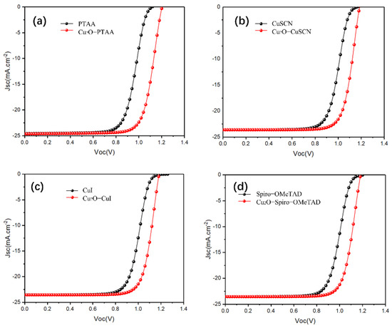
Figure 4.
(a–d) The current density-voltage (J–V) characteristic curves of both device structures (with and without a Cu2O buffer layer) with PTAA-HTL (a), CuSCN-HTL (b), CuI-HT (c), Spiro-OMeTAD (d).
Table 4.
Photovoltaic parameters obtained using different HTLs.
After testing several different HTMs using the structure of this work, we noticed that the PTAA-HTL based device exhibited a remarkable PCE of 22.49% greater than the other HTMs-based devices. Compared to the Spiro-OMeTAD-HTL device (Voc = 1.18 V, Jsc = 23.55 mA/cm2), we obtained a higher Voc, Jsc (1.20 V and 24.64 mA/cm2). The PTAA-HTM has the deepest valence band energy level with respect to MAPbI3 and Cu2O when compared with other HTMs (Figure 5), which allowed for the maximization of the Voc, and the large optical band gap (Eg = 2.95 eV) of PTAA guarantees high hole blocking properties to prevent the transfer of photogenerated charges from perovskite to itself. The valence band maximum (VBM) of MAPbI3, PTAA-HTL, and Cu2O buffer layer are 5.45 eV, 5.25 eV, and 5.37 eV, respectively. Therefore, the energy-level offset (ΔE) for charge transfer between the VBM of MAPbI3 perovskite and PTAA-HTL is 0.20 eV, and the energy-level offset (ΔE) between the VBM of PTAA-HTL and the buffer is 0.12 eV. Additionally, the Voc was also increased (without Cu2O: Voc = 1.12 V, with Cu2O: Voc = 1.20 V), perhaps due to the decrease of recombination [52]. The wide gap band of Cu2O reduces recombination losses and pulls holes from the absorber, allowing for smoother extraction of the holes while experiencing lower resistance [53]. Meanwhile, Albert et al. found that the deposition of CuOx does not degrade the surface of perovskite or introduce traps at the interface by adding a layer of CuOx between the PTAA and the anode [54].
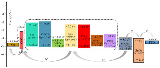
Figure 5.
Energy diagram for devices with different HTLs.
The CuSCN-HTL and CuI-HTL devices have the second-highest and third-highest efficiency of 21.70% and 21.58% (Table 4), respectively; here, the VBM of CuSCN and CuI are equivalent to that of Spiro-OMeTAD (Figure 5), but they have better hole mobility than Spiro-OMeTAD (Table 1, Table 4). Therefore, the addition of the Cu2O buffer layer has even balanced the VBM of CuSCN-HTL and CuI-HTL, which enhances the device performance after replacing the Spiro-OMeTAD (the PCE of the Cu2O/Spiro-OMeTAD device is 21.46%), It is worth noting that the addition of the Cu2O buffer layer has a simultaneous “slight” S-bend elimination effect on the PEDOT: PSS-HTL and P3HT-HTL devices, while it negatively affects CuSbSe2 (Figure S2). These phenomena can be attributed to their small band gaps. Compared to PTAA, despite having a close VBM, their lower conduction band minimum (CBM) leads to electron leakage from the perovskite absorber layer to the anode. The higher CBM of Cu2O helps to prevent electron leakage from the perovskite to the metal electrode, which may reduce the recombination of the HTL, the electrode, and the related interfaces, thereby reducing unnecessary Voc loss.
Consequently, compared to other HTMs, since PTAA has the deepest VBM and a suitable bandgap, the Cu2O material can achieve the best energy alignment with PTAA and MAPbI3, which makes the Cu2O well suited as a buffer layer in n-i-p structured perovskite devices [55].
3.4. The Optimization of Cu2O, Absorber Layer, and PTAA Thickness
According to the previous research shown in Section 3.3, based on the most effective structure of Cu/Cu2O/PTAA, the optimized thickness combinations were still absent in our study. Hence, first, we kept the thickness of PTAA-HTL at 0.15 µm, the tunable thickness of the Cu2O buffer layer (from 0.01 µm to 0.10 µm) and the absorber layer (from 0.40 µm to 1.0 µm), and Jsc, Voc, FF and PCE were carried out; all results are summarized in Figure 6.
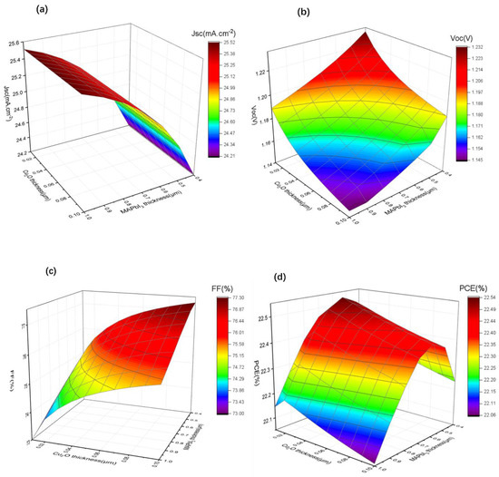
Figure 6.
(a–d) The variation of Jsc, Voc, FF, and PCE with different perovskite layer (0.4 µm to 1 µm) and Cu2O buffer layer (0.01 µm to 0.1 µm) thicknesses.
As shown in Figure 6a, the Jsc changed slightly with the change in thickness of Cu2O, probably owning to the fact that the use of a thinner Cu2O will not affect the photo absorption. The photocurrent decreased from 25.45 mA/cm2 to around 24.20 mA/cm2 as the thickness of MAPbI3 decreased because the thinner absorption layer absorbs fewer photons, resulting in fewer electron-hole pairs. Conversely, the Voc shows an increasing tendency when the thickness of MAPbI3 and Cu2O decreases (Figure 6b), which may be due to the reduced recombination of free charge carriers in thinner function layers. We find that FF (Figure 6c) decreases with the decreasing thickness of Cu2O, which may be due to the fact that thinner Cu2O is less effective in improving charge accumulation. However, it increases with the decreasing thickness of MAPbI3 because thinner MAPbI3 results in lower series resistance of the device. Combined with the changes of Jsc and Voc, it can be seen from Figure 6d that PCE increases with the decrease in Cu2O thickness until it is close to 0.02 µm, and it shows a clear trend of first rising and then falling with the decrease inMAPbI3 thickness, reaching the maximum value at 0.60 µm.
Based on the previous research, the optimized buffer layer thickness and absorber layer thickness are kept constant to obtain the optimal thickness of the PTAA. We changed the thickness of the PTAA from 0.01 µm to 1.0 µm (Figure 7), and we see that Jsc remains almost unchanged when the PTAA thickness is greater than 0.02 µm; Voc increases slowly as the PTAA thickness increases. PCE and FF decrease continuously when the PTAA thickness is greater than 0.02 µm, which may be due to higher series resistance with increasing PTAA thickness. It was found that the maximum PCE of the device was 22.94% when the thickness of PTAA was 0.02 µm.
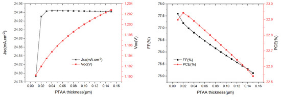
Figure 7.
The variation of Jsc, Voc, FF, and PCE with different PTAA-HTL layer (0.01 µm to 0.15 µm) thicknesses.
Through our optimization, the device can achieve the best performance when the thickness of Cu2O, MAPbI3, and PTAA are 0.02, 0.60, and 0.02 µm, respectively, and the maximum PCE is 22.94%, FF is 77.20%, Jsc is 24.93 mA/cm2, and Voc is 1.19V.
3.5. The Effect of Interface Layer Defect
The impact of the defect states in both interfaces in the proposed structure of the cell, the HTL/absorber, and the absorber/ETL have been investigated in detail. The defect parameters of the two interface layers are shown in Table S1.
The influence of the defect density at the PTAA/absorber interface layer on the solar cell parameters was changed from 109 cm−2 to 1013 cm−2, while the other variables remained unchanged. The results we obtained are as shown in Figure 8. We can see that the increase in the defect density results in a decrease in the Voc, Jsc and PCE, while the FF shows an upward trend. In regards to FF as the ratio of maximum power area to the product of Jsc and Voc in the J–V curve, its increase may be attributed to a slightly unchanged maximum power point (MPP) when both Jsc and Voc decrease. Notably, FF cannot be used as the primary parameter representing cell performance. Increasing the interface defect density accelerates the recombination rate of charge carrier at the PTAA/absorber interface, which results in degraded device performance. Thus, a value of defect density of 1 × 109 cm−2 could be chosen as a design parameter, yielding PCE = 22.94%.
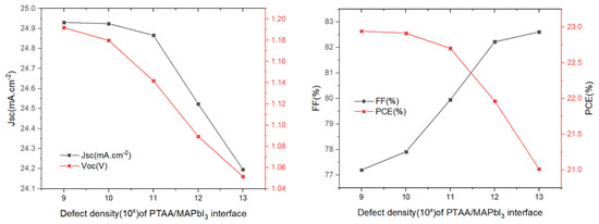
Figure 8.
Influence of the HTL/absorber interface defect density on the photovoltaic parameters (Voc, Jsc, FF, and PCE).
Next, we studied the effect of defect density regarding the absorber/ETL interface (Figure 9). It has a substantial influence on the function of the solar cells, as the quality of the absorber/ETL interface exhibits a significant impact on PSCs performance. The results are shown in Figure 9. It can be observed that several parameters change very little in the defect density range from 109 to 1011 cm−2, and then drop abruptly when the defect density in in a range greater than 1011 cm−2. Such a sharp decline in solar cell performance can be attributed to the increase in recombination. Therefore, in order to maintain high efficiency, the defect density should be controlled in the range of 109 to 1011 cm−2. A defect density of 1 × 109 cm−2 was chosen and, in this case, PCE = 22.94%.
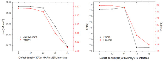
Figure 9.
Influence of the MAPbI3/SnO2 interface defect density on the photovoltaic parameters (Voc, Jsc, FF, and PCE).
4. Conclusions
In conclusion, we proposed the inclusion of an inorganic material (Cu2O) into perovskite solar cells as a buffer layer between the HTL and the electrode. We found that the insertion of Cu2O can greatly improve the FF of n-i-p devices for low work function electrodes (especially Cu), which is attributed to the fact that it can effectively lower the interfacial energy barrier between the interface and promote hole transportation. Simultaneously, it can achieve the best energy alignment among Cu, Cu2O, and PTAA, thereby reducing the charge accumulation, which optimizes Voc and PCE. Moreover, we optimized the thickness of Cu2O, MAPbI3, and PTAA to 0.02 µm, 0.60 µm, and 0.02 µm, respectively, and the appropriate defect densities at the interface between the HTL/absorber and absorber/ETL were explored to provide a reference for the experiment. The most efficient performance device we achieved showed a PCE of 22.94%, Jsc of 24.93 mA/cm2, Voc of 1.19V, and FF of 77.04%, This simulation study has instructive implications for achieving high efficiency, as well as low-cost perovskite solar cells.
Supplementary Materials
The following supporting information can be downloaded at: https://www.mdpi.com/article/10.3390/ma15228142/s1, Figure S1: Absorption coefficient curves of FTO, SnO2, MAPI3, Cu2O and HTLs. The data used to plot these curves are obtained from results reported (FTO [56], SnO2 [57], MAPbI3 [58], Spiro-OMeTAD [59], Cu2O [60], CuI [61], CuSCN [62], CuSbSe2 [47], PTAA [63], PEDOT:PSS [64], P3HT [65]); Figure S2: Current density- voltage (J-V) characteristic curves of both ideal device structures (with and without Cu2O buffer layer) with PEDOT: PSS, P3HT, and CuSbSe2 HTLs; Table S1: Parameters of interface layer; Table S2: Parameters of back and front contacts; Table S3: Work Function of Back Metal electrode [66,67].
Author Contributions
Conceptualization, C.L. and G.L.; Methodology, B.Z., D.P.d.L. and H.Z.; Supervision, G.L. and L.W.; Formal analysis, Q.W., Q.S. and M.L.; Writing—original draft, C.L., G.L., L.W. and X.X.; Writing—review & editing, C.L., G.L., X.X., L.W., Q.W., Q.S., M.L., B.Z., D.P.d.L. and H.Z. Funding acquisition, G.L. and X.X. All authors have read and agreed to the published version of the manuscript.
Funding
This research was funded by National Natural Science Foundation of China (No.52202241) and Leading Innovative and Entrepreneur Team of Zhejiang (No.2019R01012).
Institutional Review Board Statement
Not applicable.
Informed Consent Statement
Not applicable.
Data Availability Statement
Not applicable.
Acknowledgments
The authors would like to acknowledge Marc Burgelman from the University of Gent for providing free access to the SCAPS simulation software.
Conflicts of Interest
The authors declare no conflict of interest.
References
- Stranks, S.; Eperon, G.; Grancini, G.; Menelaou, C.; Alcocer, M.; Leijtens, T.; Herz, L.; Petrozza, A.; Snaith, H. Electron-Hole Diffusion Lengths Exceeding 1 Micrometer in an Organometal Trihalide Perovskite Absorber. Science 2013, 342, 341–344. [Google Scholar] [CrossRef] [PubMed]
- Shrotriya, V.; Li, G.; Yao, Y.; Chu, C.; Yang, Y. Transition metal oxides as the buffer layer for polymer photovoltaic cells. Appl. Phys. Lett. 2006, 88, 073508. [Google Scholar] [CrossRef]
- Chen, Y.; Tang, Y.; Chen, P.; Zhang, L.; Liu, Q.; Zhao, Y.; Huang, Q.; Zhang, X. Progress in perovskite solar cells based on different buffer layer materials. Acta. Phys. Sin. 2020, 69, 138401. [Google Scholar] [CrossRef]
- Arora, N.; Dar, M.; Hinderhofer, A.; Pellet, N.; Schreiber, F.; Zakeeruddin, S.; Gratzel, M. Perovskite solar cells with CuSCN hole extraction layers yield stabilized efficiencies greater than 20%. Science 2017, 358, 768–771. [Google Scholar] [CrossRef]
- Zhou, J.; Liu, P.; Du, Y.; Zong, W.; Zhang, B.; Liu, Y.; Xu, S.; Cao, S. Evident Enhancement of Efficiency and Stability in Perovskite Solar Cells with Triphenylamine-Based Macromolecules on the CuSCN Hole-Transporting Layer. J. Electron. Mater. 2021, 50, 3962–3971. [Google Scholar] [CrossRef]
- Zilberberg, K.; Meyer, J.; Riedl, T. Solution processed metal-oxides for organic electronic devices. J. Mater. Chem. C 2013, 1, 4796–4815. [Google Scholar] [CrossRef]
- Cai, C.; Zhou, K.; Guo, H.; Pei, Y.; Hu, Z.; Zhang, J.; Zhu, Y. Enhanced Hole extraction by NiO Nanoparticles in carbon-based perovskite solar cells. Electrochim. Acta. 2019, 312, 100–108. [Google Scholar] [CrossRef]
- Zhao, Y.; Nardes, A.; Zhu, K. Effective hole extraction using MoOx-Al contact in perovskite CH3NH3PbI3 solar cells. Appl. Phys. Lett. 2014, 104, 213906. [Google Scholar] [CrossRef]
- Gnaser, H. Energy and Angular Distributions of Sputtered Species. Sputtering by Particle Bombardment; Behrisch, R., Eckstein, W., Eds.; Springer: Berlin/Heidelberg, Germany, 2007; Volume 110, pp. 231–328. [Google Scholar]
- Hou, Y.; Du, X.; Scheiner, S.; McMeekin, D.P.; Wang, Z.; Li, N.; Killian, M.S.; Chen, H.; Richter, M.; Levchuk, I.; et al. A Generic Interface to Reduce the Efficiency-Stability-Cost Gap of Perovskite Solar Cells. Science 2017, 358, 1192–1197. [Google Scholar] [CrossRef]
- Ramos, F.; Jutteau, S.; Posada, J.; Bercegol, A.; Rebai, A.; Guillemot, T.; Bodeux, R.; Schneider, N.; Loones, N.; Ory, D.; et al. Highly Efficient MoOx-Free Semitransparent Perovskite Cell for 4 T Tandem Application Improving the Efficiency of Commercially-Available Al-BSF Silicon. Sci. Rep. 2018, 8, 16139. [Google Scholar] [CrossRef]
- Wang, Y.; Xia, Z.; Liang, J.; Wang, X.; Liu, Y.; Liu, C.; Zhang, S.; Zhou, H. Towards printed perovskite solar cells with cuprous oxide hole transporting layers: A theoretical design. Semicond. Sci. Technol. 2015, 30, 054004. [Google Scholar] [CrossRef]
- Kim, J.; Liang, P.; Williams, S.; Cho, N.; Chueh, C.; Glaz, M.; Ginger, D.; Jen, A. High-Performance and Environmentally Stable Planar Heterojunction Perovskite Solar Cells Based on a Solution-Processed Copper-Doped Nickel Oxide Hole-Transporting Layer. Adv. Mater. 2015, 27, 695–701. [Google Scholar] [CrossRef] [PubMed]
- Chatterjee, S.; Pal, A. Introducing Cu2O Thin Films as a Hole-Transport Layer in Efficient Planar Perovskite Solar Cell Structures. J. Phys. Chem. C 2016, 120, 1428–1437. [Google Scholar] [CrossRef]
- Iivonen, T.; Heikkila, M.J.; Popov, G.; Nieminen, H.; Kaipio, M.; Kemell, M.; Mattinen, M.; Meinander, K.; Mizohata, K.; Raisanen, J.; et al. Atomic Layer Deposition of photoconductive Cu2O Thin Films. ACS Omega. 2019, 4, 11205–11214. [Google Scholar] [CrossRef] [PubMed]
- Islam, M.; Sobayel, K.; Al-Kahtani, A.; Islam, M.; Muhammad, G.; Amin, N.; Shaiduzzaman, M.; Akhtaruzzaman, M. Defect Study and Modelling of SnX3-Based Perovskite Solar Cells with SCAPS-1D. Nanomaterials 2021, 11, 1218. [Google Scholar] [CrossRef] [PubMed]
- Du, H.; Wang, W.; Zhu, J.Z. Device simulation of lead-free CH3NH3SnI3 perovskite solar cells with high efficiency. Chin. Phys. B 2016, 25, 108802. [Google Scholar] [CrossRef]
- Jannat, F.; Ahmed, S.; Alim, M. Performance analysis of cesium formamidinium lead mixed halide based perovskite solar cell with MoOx as hole transport material via SCAPS-1D. Optik 2021, 228, 166202. [Google Scholar] [CrossRef]
- Raoui, Y.; Ez-Zahraouy, H.; Tahiri, N.; El Bounagui, O.; Ahmad, S.; Kazim, S. Performance analysis of MAPbI (3) based perovskite solar cells employing diverse charge selective contacts: Simulation study. Sol. Energy 2019, 193, 948–955. [Google Scholar] [CrossRef]
- Du, H.; Wang, W.; Gu, Y. Simulation design of P–I–N-type all-perovskite solar cells with high efficiency. Chin. Phys. B 2017, 26, 028803. [Google Scholar] [CrossRef]
- Karthick, S.; Boucle, J.; Velumani, S. Effect of bismuth iodide (BiI3) interfacial layer with different HTL’s in FAPI based perovskite solar cell-SCAPS-1D study. Sol. Energy 2021, 218, 157–168. [Google Scholar] [CrossRef]
- Lin, L.; Jiang, L.Q.; Li, P.; Xiong, H.; Kang, Z.; Fan, B.D.; Qiu, Y. Simulated development and optimized performance of CsPbI3 based all-inorganic perovskite solar cells. Sol. Energy 2020, 198, 454–460. [Google Scholar] [CrossRef]
- Sun, C.; Mroz, M.; Smirnov, J.; Luer, L.; Hermida-Merino, D.; Zhao, C.; Takeuchi, M.; Sugiyasu, K.; Cabanillas-Gozalez, J. Amplified spontaneous emission in insulated polythiophenes. J. Mater. Chem. C 2019, 6, 6591–6596. [Google Scholar] [CrossRef]
- Isakova, A.; Karuthedath, S.; Arnold, T.; Howse, J.; Topham, P.; Toolan, D.; Laquai, F.; Luer, L. Efficient long-range electron transfer processes in polyfluorene–perylene diimide blends. Nanoscale 2018, 10, 10934–10944. [Google Scholar] [CrossRef]
- Karuthedath, S.; Sauermann, T.; Egelhaaf, H.; Wannemacher, R.; Brabec, C.; Luer, L. The effect of oxygen induced degradation on charge carrier dynamics in P3HT: PCBM and Si-PCPDTBT: PCBM thin films and solar cells. J. Mater. Chem. A 2015, 3, 3399–3408. [Google Scholar] [CrossRef]
- Xu, W.; Daunis, T.B.; Piper, R.; Hsu, J. Effects of photonic curing processing conditions on MAPbI3 film properties and solar cell performance. ACS A.E.M. 2020, 3, 8636–8645. [Google Scholar] [CrossRef]
- Yang, W.; Noh, J.; Jeon, N.; Kim, Y.; Ryu, S.; Seo, J.; Seok, S. High-performance photovoltaic perovskite layers fabricated through intramolecular exchange. Science 2015, 348, 1234–1237. [Google Scholar] [CrossRef] [PubMed]
- Deng, K.; Chen, Q.; Li, L. Modification Engineering in SnO2 Electron Transport Layer toward Perovskite Solar Cells: Efficiency and Stability. Adv. Funct. Mater. 2020, 30, 2004209. [Google Scholar] [CrossRef]
- Li, F.; Xu, M.; Ma, X.; Shen, L.; Zhu, L.; Weng, Y.; Yue, G.; Tan, F.; Chen, C. UV Treatment of Low-Temperature Processed SnO2 Electron Transport Layers for Planar Perovskite Solar Cells. Nanoscale Res. Lett. 2018, 13, 216. [Google Scholar] [CrossRef]
- Bag, A.; Radhakrishman, R.; Nekovei, R.; Jeyakumar, R. Effect of absorber layer, hole transport layer thicknesses, and its doping density on the performance of perovskite solar cells by device simulation. Sol. Energy 2019, 196, 177–182. [Google Scholar] [CrossRef]
- Karimi, E.; Ghorashi, S. The Effect of SnO2 and ZnO on the Performance of Perovskite Solar Cells. J. Electron. Mater. 2020, 49, 364–376. [Google Scholar] [CrossRef]
- Zhao, P.; Lin, Z.; Wang, J.; Yue, M.; Su, J.; Zhang, J.; Chang, J. Numerical Simulation of Planar Heterojunction Perovskite Solar Cells Based on SnO2 Electron Transport Layer. ACS Appl. Energy Mater. 2019, 2, 4504–4512. [Google Scholar] [CrossRef]
- Li, J.; Dong, Q.; Li, N.; Wang, L. Direct Evidence of Ion Diffusion for the Silver-Electrode Induced Thermal Degradation of Inverted Perovskite Solar Cells. Adv. Energy Mater. 2017, 7, 14. [Google Scholar] [CrossRef]
- Chavali, M.; Nikolova, M. Metal oxide nanoparticles and their applications in nanotechnology. SN Appl. Sci. 2019, 1, 1–30. [Google Scholar] [CrossRef]
- Yip, H.; Hau, S.; Baek, N.; Ma, H.; Jen, A. Polymer solar cells that use self-assembled-monolayer-modified ZnO/metals as cathodes. Adv. Mater. 2008, 20, 2376. [Google Scholar] [CrossRef]
- Lin, M.Y.; Lee, C.Y.; Shiu, S.C.; Wang, J.; Sun, J.Y.; Wu, W.H.; Lin, Y.; Huang, J.; Lin, C. Sol–gel processed CuOx thin film as an anode interlayer for inverted polymer solar cells. Org. Electron. 2010, 11, 1828–1834. [Google Scholar] [CrossRef]
- Sun, J.; Zhang, Y.; Wu, J.; Yang, Q.; Yu, G.; Yang, X.; Ying, Z.; Sheng, J.; He, Y.; Shou, C. An Efficient Modification at the Hole Transporting Layer/Electrode Interface for High-Performance Ag-Electrode-Based Perovskite Solar Cells. Phys. Status Solidi A 2022, 19, 200272. [Google Scholar] [CrossRef]
- Jayan, K.; Sebastain, V. Comprehensive device modelling and performance analysis of MASnI (3) based perovskite solar cells with diverse ETM, HTM and back metal contacts. Sol. Energy 2021, 217, 40–48. [Google Scholar] [CrossRef]
- Azri, F.; Meftah, A.; Sengouga, N.; Meftah, A. Electron and hole transport layers optimization by numerical simulation of a perovskite solar cell. Sol. Energy 2019, 181, 372–378. [Google Scholar] [CrossRef]
- Zuo, L.; Guo, H.; deQuilettes, D.; Jariwala, S.; De Marco, N.; Dong, S.; Deblock, R.; Ginger, D.; Dunn, B.; Wang, M.; et al. Polymer-modified Halide Perovskite Films for Efficient and Stable Planar Heterojunction Solar Cells. Sci. Adv. 2017, 3, e1700106. [Google Scholar] [CrossRef]
- Coulibaly, A.; Oyedele, S.; Aka, B. Comparative study of lead-free perovskite solar cells using different hole transporter materials. Model. Numer. Simul. Mater. Sci. 2019, 9, 97–107. [Google Scholar] [CrossRef]
- Zhao, J.; Zheng, X.; Deng, Y.; Li, T.; Shao, Y.; Gruverman, A.; Shiled, J.; Huang, J. Is Cu a stable electrode material in hybrid perovskite solar cells for a 30-year lifetime. Energy Environ. Sci. 2016, 9, 3650–3656. [Google Scholar] [CrossRef]
- Haque, F.; Yi, H.; Lim, J.; Lim, J.; Dua, L.; Pham, H.; Sonar, P.; Uddin, A. Small molecular material as an interfacial layer in hybrid inverted structure perovskite solar cells. Mater. Sci. Semicond. Process. 2020, 108, 104908. [Google Scholar] [CrossRef]
- Jeong, M.; Choi, I.; Go, E.; Cho, Y.; Kim, M.; Lee, B.; Jeong, S.; Jo, Y.; Choi, H.; Lee, J. Stable perovskite solar cells with efficiency exceeding 24.8% and 0.3-V voltage loss. Science 2020, 369, 1615–1620. [Google Scholar] [CrossRef]
- Shi, J.; Wei, H.; Zhu, L.; Xu, X.; Xu, Y.; Lu, S.T.; Wu, H.; Luo, Y.; Li, D.; Meng, Q. S-shaped current-voltage characteristics in perovskite solar cell. Acta. Phys. Sin. 2015, 64, 038402. [Google Scholar] [CrossRef]
- Xu, Z.; Li, N.; Liu, X.; Liu, H.; Liu, G.; Chen, Q.; Zhou, H. Balancing Energy-Level Difference for Efficient n-i-p Perovskite Solar Cells with Cu Electrode. Energy Mat. Adv. 2022, 8, 9781073. [Google Scholar] [CrossRef]
- Chakraborty, K.; Choudhury, M.; Paul, S. Numerical study of Cs2TiX6 (X = Br−, I−, F− and Cl−) based perovskite solar cell using SCAPS-1D device simulation. Sol. Energy 2019, 194, 886–892. [Google Scholar] [CrossRef]
- Gupta, G.K.; Dixit, A. Simulation studies on photovoltaic response of ultrathin CuSb(S/Se) (2) ternary compound semiconductors absorber-based single junction solar cells. Int. J. Energy Res. 2021, 44, 3724–3736. [Google Scholar] [CrossRef]
- Raoui, Y.; Kazim, S.; Galagan, Y.; Ez-Zahraouy, H.; Ahmad, S. Harnessing the potential of lead-free Sn–Ge based perovskite solar cells by unlocking the recombination channels. Sustain. Energy Fuels. 2021, 5, 4661–4667. [Google Scholar] [CrossRef]
- Karimi, E.; Ghorashi, S. Investigation of the Influence of Different Hole-Transporting Materials on the Performance of Perovskite Solar Cells. Optik 2017, 130, 650–658. [Google Scholar] [CrossRef]
- Chowdhury, M.; Shahahmadi, S.; Chelvanathan, P.; Tiong, S.; Amin, N.; Techatoet, K.; Nuthammachot, N.; Chowdhuty, T.; Sulklueng, M. Effect of Deep-Level Defect Density of the Absorber Layer and n/i Interface in Perovskite Solar Cells by SCAPS-1D. Results Phys. 2020, 16, 102839. [Google Scholar] [CrossRef]
- Wu, G.; Li, X.; Zhou, J.; Zhang, J.; Zhang, X.; Leng, X.; Wang, P.; Chen, M.; Zhao, K.; Zhang, Y. Fine Multi-phase Alignments in 2D Perovskite Solar Cells with Efficiency over 17% via Slow Post-Annealing. Adv. Mater. 2019, 31, 1903889. [Google Scholar] [CrossRef] [PubMed]
- Yousuf, M.; Saeed, F.; Tauqeer, H. Numerical Investigation of Cu2O as Hole Transport Layer for High- Efficiency CIGS Solar Cell. Preprints 2021, 2021100326. [Google Scholar] [CrossRef]
- Jagt, R.; Huq, T.; Hill, S.; Thway, M.; Liu, T.; Napari, M.; Roose, B.; Galkowski, K.; Li, W.; Lin, S. Rapid vapor-phase deposition of high-mobility p-type buffer layers on perovskite photovoltaics for efficient semitransparent devices. ACS Energy Lett. 2020, 5, 2456–2465. [Google Scholar] [CrossRef]
- Kim, H.; Lim, K.; Lee, T. Planar heterojunction organometal halide perovskite solar cells: Roles of interfacial layers. Energy Environ. Sci. 2016, 9, 12–30. [Google Scholar] [CrossRef]
- Canestraro, C.; Oliveira, M.; Valaski, R.; da Silva, M.; David, D.; Pepe, I.; da Silva, A.; Roman, L.; Persson, C. Strong inter-conduction-band absorption in heavily fluorine doped tin oxide. Appl. Surf. Sci. 2008, 255, 1874–1879. [Google Scholar] [CrossRef]
- Kumar, A.; Gahlaut, P.; Gupta, N. Highly efficient tin oxide-based colloidal lead sulfide quantum dot solar cell. Energy Stor. Mater. 2022, e331. [Google Scholar] [CrossRef]
- Loper, P.; Stuckelberger, M.; Niesen, B.; Wener, J.; Filipic, M.; Moon, S.; Yum, J.; Topic, M.; De Wolf, S.; Ballif, C. Complex Refractive Index Spectra of CH3NH3PbI3 Perovskite Thin Films Determined by Spectroscopic Ellipsometry and Spectrophotometry. Jpn. J. Appl. Phys. 2015, 6, 66–71. [Google Scholar] [CrossRef]
- Chen, H.; Bryant, D.; Troughton, J.; Kirkus, M.; Neophytou, M.; Miao, X.; Durrant, J.; McCulloch, I. One-Step Facile Synthesis of a Simple Hole Transport Material for Efficient Perovskite Solar Cells. Chem. Mater. 2016, 28, 2515–2518. [Google Scholar] [CrossRef]
- Yu, W.; Li, F.; Wang, H.; Alarousu, E.; Chen, Y.; Lin, B.; Wang, L.; Hedhili, M.; Li, Y.; Wu, K. Ultrathin Cu2O as an efficient inorganic hole transporting material for perovskite solar cells. Nanoscale 2016, 8, 6173–6179. [Google Scholar] [CrossRef]
- Mohamed, S.; Gasiorowski, J.; Hingerl, K.; Zahn, D.; Scharber, M.; Obayya, A.; El-Mansy, M.; Sariciftci, N.; Egbe, D.; Stadler, P. CuI as versatile hole-selective contact for organic solar cell based on anthracene-containing PPE–PPV. Sol. Energy Mater. Sol. Cells 2015, 143, 369–374. [Google Scholar] [CrossRef]
- Liu, J.; Pathak, S.; Sakai, N.; Sheng, R.; Bai, S.; Wang, Z.; Snaith, H. Identification and Mitigation of a Critical Interfacial Instability in Perovskite Solar Cells Employing Copper Thiocyanate Hole-Transporter. Adv. Mater. Interfaces 2016, 3, 1600571. [Google Scholar] [CrossRef]
- Masumura, K.; Nakanishi, I.; Khuat, K.; Kinashi, K.; Sakai, W.; Tsutsumi, N. Optimal composition of the poly(triarylamine)-based polymer composite to maximize photorefractive performance. Sci. Rep. 2019, 9, 739. [Google Scholar] [CrossRef] [PubMed]
- Ahmed, R. Effect of Gold Nanoparticles on the Physical Properties of Poly (3,4-ethylenendioxythiophene): Poly (styrene sulphonate) and its Gas Sensor Application. Arab J. Nuc. Sci. Appl. 2018, 51, 9–18. [Google Scholar] [CrossRef]
- Cook, S.; Furube, A.; Katoh, R. Analysis of the excited states of regioregular polythiophene P3HT. Energy Environ. Sci. 2008, 1, 294–299. [Google Scholar] [CrossRef]
- Ming, W.; Yang, D.; Li, T.; Zhang, L.; Du, M. Formation and Diffusion of Metal Impurities in Perovskite Solar Cell Material CH3NH3PbI3: Implications on Solar Cell Degradation and Choice of Electrode. Adv. Sci. 2018, 5, 1700662. [Google Scholar] [CrossRef] [PubMed]
- Kanoun, A.; Kanoun, B.; Merad, A.; Goumri-Said, S. Toward development of high-performance perovskite solar cells based on CH3NH3GeI3 using computational approach. Sol. Energy 2019, 182, 237–244. [Google Scholar] [CrossRef]


Publisher’s Note: MDPI stays neutral with regard to jurisdictional claims in published maps and institutional affiliations. |
© 2022 by the authors. Licensee MDPI, Basel, Switzerland. This article is an open access article distributed under the terms and conditions of the Creative Commons Attribution (CC BY) license (https://creativecommons.org/licenses/by/4.0/).