
Technology and Reliability of Normally-Off GaN HEMTs with p-Type Gate


Abstract
:1. Introduction
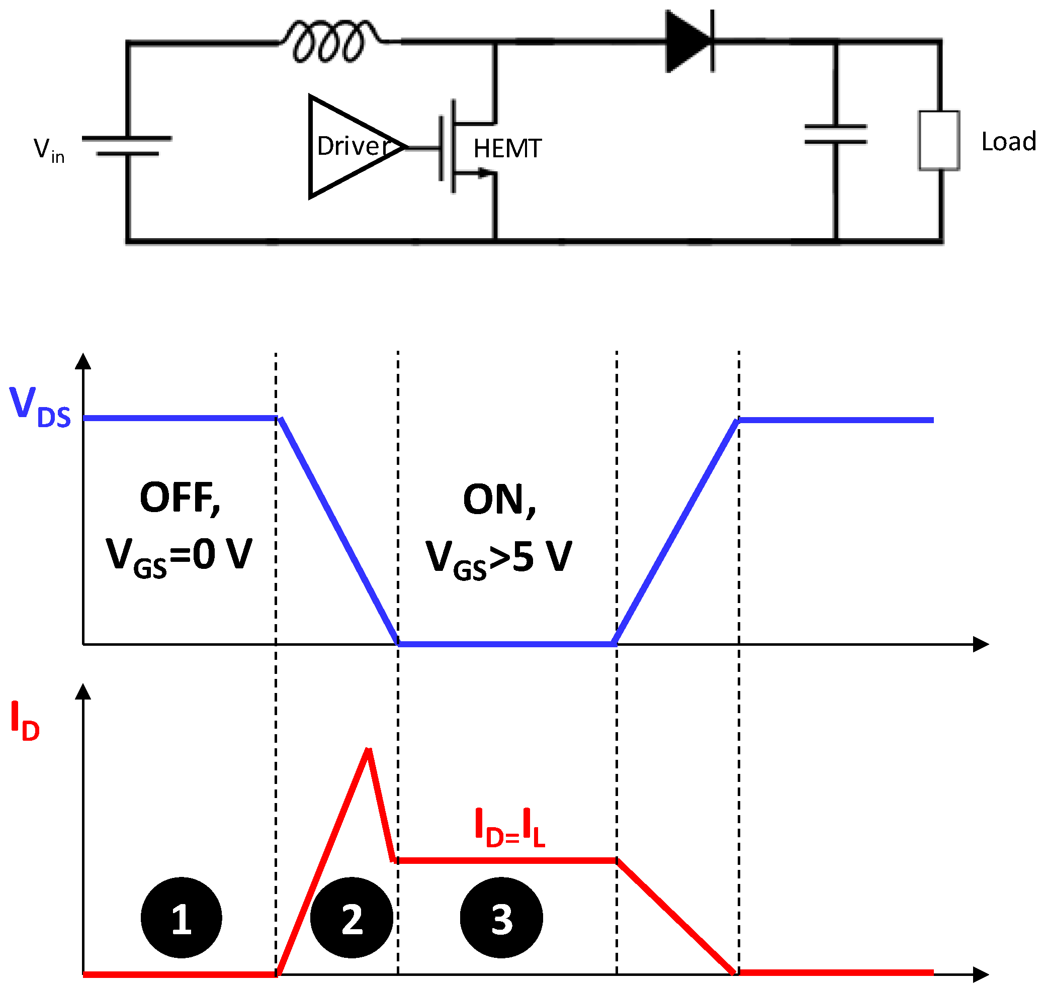
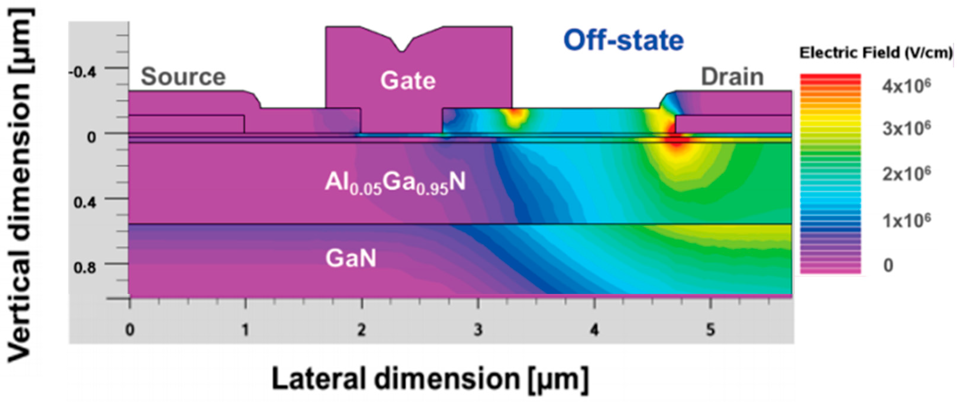
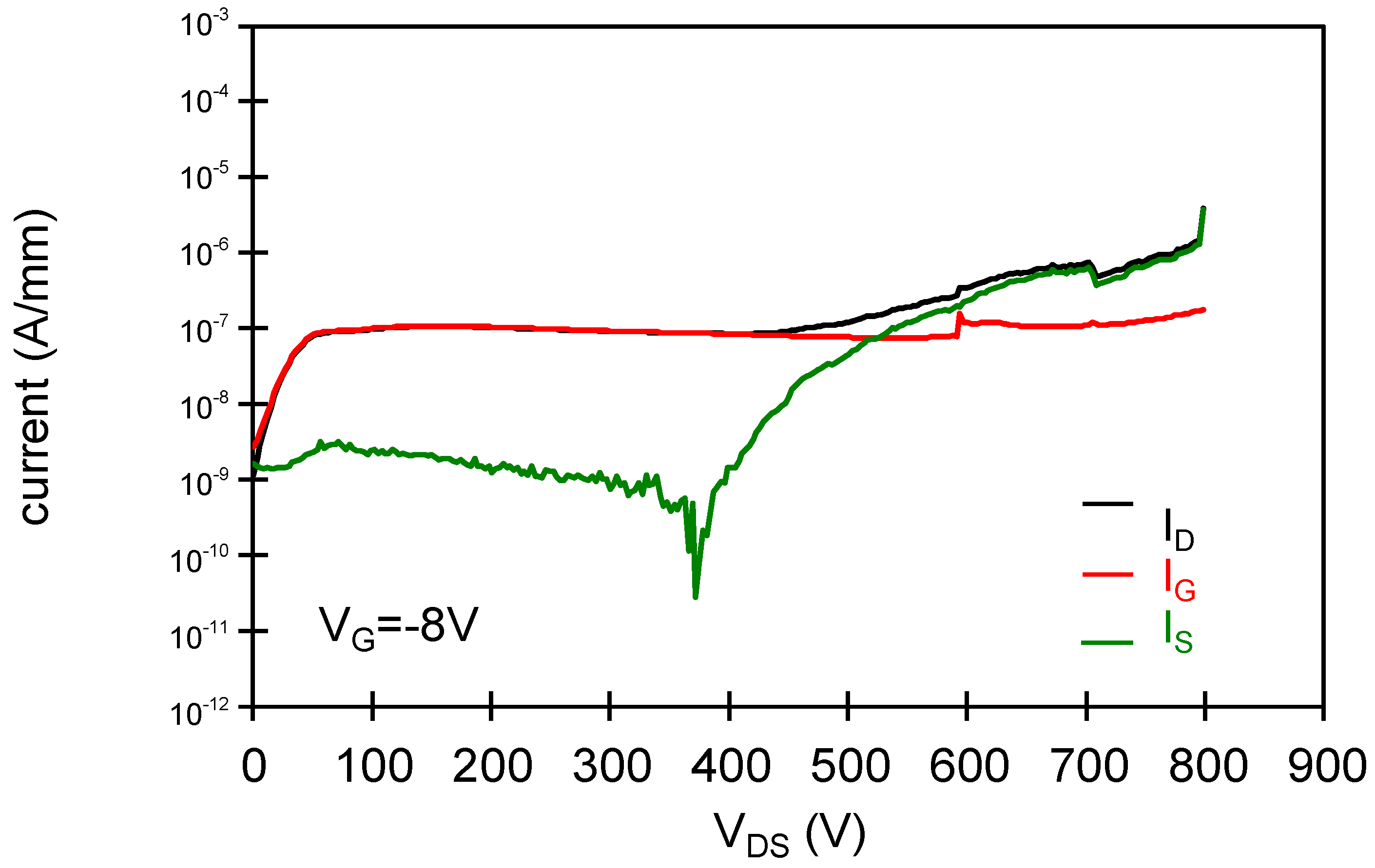
- When the transistor is in the off-state (condition (1) in Figure 1), a high drain-source voltage is applied to the HEMT. The high resulting field (Figure 2) may favor charge trapping mechanisms, including the filling/depletion of defects located in the C-doped buffer [6], the injection of electrons from the substrate [7], and surface trapping processes [8]. These mechanisms are typically fully recoverable. In addition, the exposure to high off-state bias may trigger time-dependent degradation processes that lead to the catastrophic failure of the transistors [9]
- In principle, when the HEMT is used as a switch, current and voltage should never be high simultaneously. However, in a hard switching event (labeled as (2) in Figure 1), during the turn-on of the transistor the drain current can start to increase before the drain-source voltage of the HEMT drops. During the turn-on transient, the drain current can exceed the inductor current IL, due to the discharge of the drain capacitance through the channel (as explained in [5]), and then become (approximately) equal to the inductor current IL. This may favor the degradation processes triggered by hot electrons [10], and lead to an increased power dissipation (and self-heating)
- When the HEMT is in the on-state (condition labeled as (3) in Figure 1), the gate-source junction is positively biased, at voltages in the range 5–7 V. Under these conditions, the gate junction—typically based on an MIS-stack or on a p-GaN layer—may show a time-dependent degradation [11] that leads to a strong increase in gate leakage
- The non-ideality of the switching events (i.e., the fact that current and voltage may be high simultaneously) may increase the peak and average power dissipation, and thus the self-heating. Operation at higher temperatures may further accelerate the trapping and degradation processes described above, thus limiting device lifetime.
- (i)
- The implantation of fluorine ions under the gate [12]. The negative charge of the F-ions favors the depletion of the channel, and results in a positive threshold voltage Vth. Recent papers [13,14] showed that F-ions may show instability under high electrical stress, thus leading to changes in the threshold voltage. Chen et al. [15] indicate that on recent devices an excellent stability of fluorine atoms can be obtained through F-plasma ion implantation.
- (ii)
- The use of a MIS-type gate stack, with full recess of the AlGaN [16]. This solution guarantees an effective minimization of the gate leakage, and threshold voltages higher than one volt. The main drawbacks of this approach are the threshold voltage instability (positive (PBTI) [17], or negative (NBTI) [18]) due to the interface/border traps in the insulator, and the time-dependent dielectric breakdown (TDDB) of the thin insulator [11].
- (iii)
- The integration, in a single package, of a cascoded pair constituted by a (normally-on) high voltage GaN-transistor and a low voltage silicon MOSFET [19]. The latter controls the on/off state of the pair, while the GaN HEMT (that has a high robustness to high fields) holds the voltage in the off-state. The advantages of this solution are the very good stability of the threshold voltage, the possibility of using standard Si drivers, and the use of a normally-on HEMT, whose fabrication process and reliability are well assessed. On the other hand, cascode complexity is the main drawback of the cascoded solution.
- (iv)
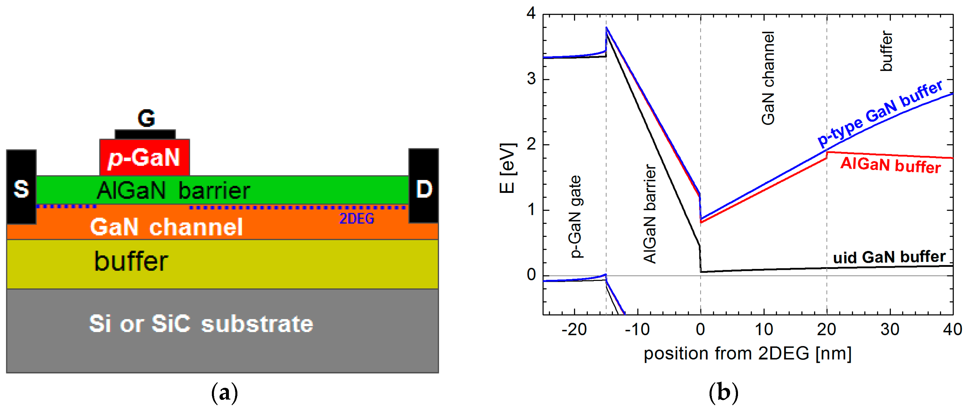
- The use of a p-GaN or p-AlGaN layer on top of the AlGaN/GaN heterojunction. The p-type layer lifts the band diagram of the heterostructure, and this results in a complete depletion of the 2DEG with VGS = 0 V. Specific issues of HEMTs with p-GaN gate are the time-dependent degradation of the gate-stack, and trapping effects related to the Mg-acceptor.
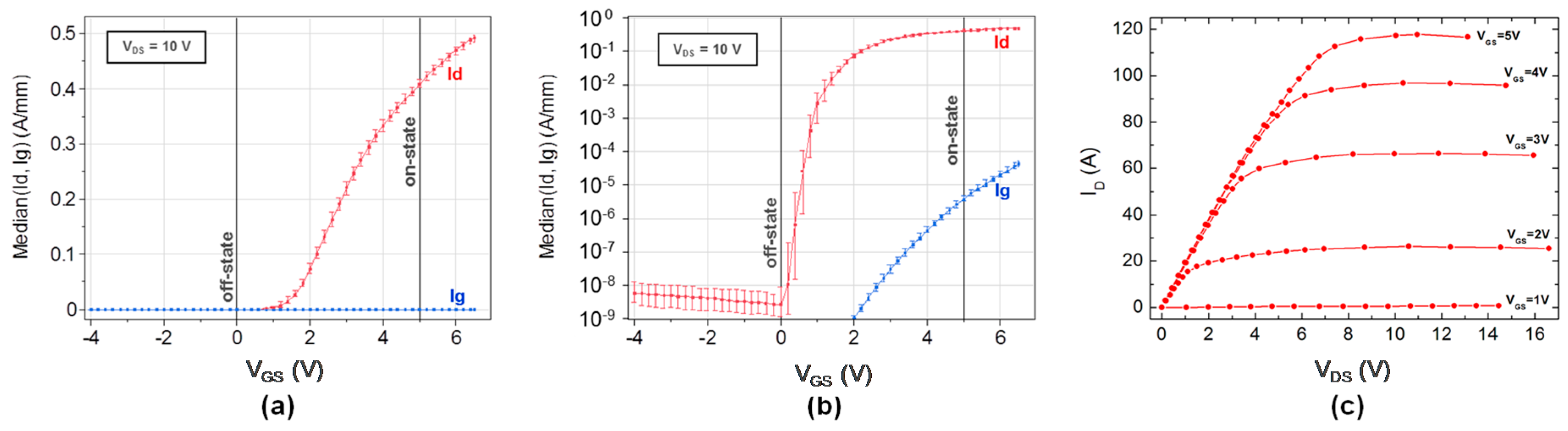
2. Normally-Off Transistors with p-GaN Gate: Technology and Performance
3. Recoverable and Permanent Degradation of Normally-Off Transistors with p-GaN Gate
3.1. Charge Trapping Processes Related to the p-GaN Gate
3.2. Degradation Processes Induced by Positive Gate Bias
3.3. Degradation Processes Induced by High Drain Bias in the Off-State
4. Conclusions
Acknowledgments
Author Contributions
Conflicts of Interest
References
- Herbecq, N.; Roch-Jeune, I.; Rolland, N.; Visalli, D.; Derluyn, J.; Degroote, S.; Germain, M.; Medjdoub, F. 1900 V, 1.6 mΩ·cm2 AlN/GaN-on-Si power devices realized by local substrate removal. Appl. Phys. Express 2014, 7, 034103. [Google Scholar] [CrossRef]
- Chen, J.; Persson, I.; Nilsson, D.; Hsu, C.; Palisaitis, J.; Forsberg, U.; Per, O.Å.; Janzén, E. Room-temperature mobility above 2200 cm2/V·s of two-dimensional electron gas in a sharp-interface AlGaN/GaN heterostructure. Appl. Phys. Lett. 2015, 106. [Google Scholar] [CrossRef]
- GS66516T Datasheet. Available online: http://www.gansystems.com/datasheets/GS66508T%20DS%20Rev%20161101.pdf (accessed on 19 January 2017).
- Morita, T.; Tamura, S.; Anda, Y.; Ishida, M.; Uemoto, Y.; Ueda, T.; Tanaka, T.; Ueda, D. 99.3% Efficiency of Three-Phase Inverter for Motor Drive Using GaN-based Gate Injection Transistors. In Proceedings of the 2011 Twenty-Sixth Annual IEEE Applied Power Electronics Conference and Exposition (APEC), Fort Worth, TX, USA, 6–11 March 2011; pp. 481–484.
- Bahl, S.R.; Ruiz, D.; Lee, D.S. Product-level Reliability of GaN Devices. In Presented at the IEEE International Reliability Physics Symposium, Pasadena, CA, USA, 17–21 April 2016.
- Moens, P.; Banerjee, A.; Uren, M.J.; Meneghini, M.; Karboyan, S.; Chatterjee, I.; Vanmeerbeek, P.; Cäsar, M.; Liu, C.; Salih, A.; et al. Impact of buffer leakage on intrinsic reliability of 650 V AlGaN/GaN HEMTs. In Proceedings of the IEEE Electron Devices Meeting, Washington, DC, USA, 7 December 2015; pp. 903–906.
- Bisi, E.Z.D.; Meneghini, M.; Marino, F.A.; Marcon, D.; van Hove, S.S.M.; Decoutere, S.; Meneghesso, G. Kinetics of Buffer-Related R ON-Increase in GaN-on-Silicon MIS-HEMTs. IEEE Electron Device Lett. 2014, 35, 1004–1006. [Google Scholar] [CrossRef]
- Meneghesso, G.; Meneghini, M.; Rossetto, I.; Bisi, D.; Stoffels, S.; Van Hove, M.; Decoutere, S.; Zanoni, E. Reliability and parasitic issues in GaN-based power HEMTs: A review. Semicond. Sci. Technol. 2016, 31, 093004. [Google Scholar] [CrossRef]
- Meneghini, M.; Rossetto, I.; Hurkx, G.A.M.; Sonsky, J.; Croon, J.A.; Meneghesso, G.; Zanoni, E. Extensive Investigation of Time-Dependent Breakdown of GaN-HEMTs Submitted to Off-State Stress. IEEE Trans. Electron Devices 2015, 62, 2549–2554. [Google Scholar] [CrossRef]
- Ruzzarin, M.; Meneghini, M.; Member, S.; Rossetto, I.; Van Hove, M.; Stoffels, S.; Wu, T.; Decoutere, S.; Meneghesso, G. Evidence of Hot-Electron Degradation in GaN-based MIS-HEMTs Submitted to High Temperature Constant Source Current Stress. IEEE Electron Device Lett. 2016, in press. [Google Scholar] [CrossRef]
- Wu, T.; Marcon, D.; De Jaeger, B.; Van Hove, M.; Bakeroot, B.; Stoffels, S.; Groeseneken, G.; Decoutere, S.; Roelofs, R. Time dependent dielectric breakdown (TDDB) evaluation of PE-ALD SiN gate dielectrics on AlGaN/GaN recessed gate D-mode MIS-HEMTs and E-mode MIS-FETs. In Proceedings of the IEEE International Reliability Physics Symposium, Monterey, CA, USA, 19–23 April 2015.
- Ma, C.; Chen, H.; Zhou, C.; Huang, S.; Yuan, L.; Roberts, J.; Chen, K.J. ON-state critical gate overdrive voltage for fluorine-implanted enhancement-mode AlGaN/GaN high electron mobility transistors. J. Appl. Phys. 2011, 110, 114514. [Google Scholar] [CrossRef]
- Wang, M.J.; Yuan, L.; Chen, K.J.; Xu, F.J.; Shen, B. Diffusion mechanism and the thermal stability of fluorine ions in GaN after ion implantation. J. Appl. Phys. 2009, 105, 083519. [Google Scholar] [CrossRef]
- Bisi, D.; Meneghini, M.; Stocco, A.; Cibin, G.; Pantellini, A.; Nanni, A.; Lanzieri, C.; Zanoni, E.; Meneghesso, G. Influence of Fluorine-based Dry Etching on Electrical Parameters of AlGaN/GaN-on-Si High Electron Mobility Transistors. In Proceedings of the European Solid-State Device Research Conference (ESSDERC), Bucharest, Romania, 16–20 September 2013; pp. 61–64.
- Chen, K.J.; Zhou, C. Enhancement-mode AlGaN/GaN HEMT and MIS-HEMT technology. Phys. Status Solidi Appl. Mater. 2011, 208, 434–438. [Google Scholar] [CrossRef]
- Wu, T.; Marcon, D.; De Jaeger, B.; Van Hove, M.; Bakeroot, B.; Lin, D.; Kang, X.; Roelofs, R.; Groeseneken, G.; Decoutere, S. The impact of the gate dielectric quality in developing Au-free D-mode and E-mode recessed gate AlGaN/GaN transistors on a 200 mm Si substrate. In Proceedings of the 27th International Symposium on Power Semiconductor Devices and ICs, Kowloon Shangri-La, Hong Kong, China, 10–14 May 2015; pp. 225–228.
- Lagger, P.; Reiner, M.; Pogany, D.; Ostermaier, C. Comprehensive study of the complex dynamics of forward bias-induced threshold voltage drifts in GaN based MIS-HEMTs by stress/recovery experiments. IEEE Trans. Electron Devices 2014, 61, 1022–1030. [Google Scholar] [CrossRef]
- Meneghini, M.; Rossetto, I.; Bisi, D.; Ruzzarin, M.; Van Hove, M.; Stoffels, S.; Wu, T.; Marcon, D.; Decoutere, S.; Meneghesso, G.; et al. Negative Bias-Induced Threshold Voltage Instability in GaN-on-Si Power HEMTs. IEEE Electron Device Lett. 2016, 37, 474–477. [Google Scholar] [CrossRef]
- Hirose, T.; Imai, M.; Joshin, K.; Watanabe, K.; Ogino, T.; Miyazaki, Y.; Shono, K.; Hosoda, T.; Asai, Y. Dynamic performances of GaN-HEMT on Si in cascode configuration. In Proceedings of the 2014 Twenty-Ninth Annual IEEE Applied Power Electronics Conference and Exposition, Fort Worth, TX, USA, 16–20 March 2014; pp. 174–181.
- Hilt, O.; Knauer, A.; Brunner, F.; Würfl, J. Normally-off AlGaN/GaN HFET with p-type GaN Gate and AlGaN Buffer. In Proceedings of the 22nd International Symposium on Power Semiconductor Devices and ICs, Hiroshima, Japan, 16–18 March 2010.
- Hu, X.; Simin, G.; Yang, J.; Khan, M.A.; Gaska, R.; Shur, M.S. Enhancement mode AlGaN/GaN HFET with selectively grown pn junction gate. Electron. Lett. 2000, 36, 753–754. [Google Scholar] [CrossRef]
- Uemoto, Y.; Hikita, M.; Ueno, H.; Matsuo, H.; Ishida, H.; Yanagihara, M.; Ueda, T.; Ueda, D.; Tanaka, T. Gate Injection Transistor (GIT)—A Normally-Off AlGaN/GaN Power Transistor Using Conductivity Modulation. IEEE Trans. Electron Devices 2007, 54, 3393–3399. [Google Scholar] [CrossRef]
- Okita, H.; Hikita, M.; Nishio, A.; Sato, T.; Matsunaga, K. Through Recessed and Regrowth Gate Technology for Realizing Process Stability of GaN-GITs. In Proceedings of the 28th International Symposium on Power Semiconductor Devices and ICs, Prague, Czech Republic, 12–16 June 2016; pp. 23–26.
- Hilt, O.; Zhytnytska, R.; Böcker, J.; Bahat-Treidel, E.; Brunner, F.; Knauer, A. 70 mΩ/600 V Normally-off GaN Transistors on SiC and Si Substrates. In Proceedings of the 27th International Symposium on Power Semiconductor Devices and ICs, Kowloon Shangri-La, Hong Kong, China, 10–14 May 2015; pp. 237–240.
- Kim, J.; Hwang, S.; Hwang, I.; Choi, H.; Chong, S.; Choi, H.; Jeon, W.; Soon, H.; Kim, J.Y.; Park, Y.H.; et al. High Threshold Voltage p-GaN Gate Power Devices on 200 mm Si. In Proceedings of the 25th International Symposium on Power Semiconductor Devices and ICs, Kanazawa, Japan, 26–30 May 2013.
- Kaneko, N.; Machida, O.; Yanagihara, M.; Iwakami, S.; Baba, R.; Goto, H.; Iwabuchi, A. Normally-off AlGaN/GaN HFETs using NiO × Gate with Recess. In Proceedings of the 21st International Symposium on Power Semiconductor Devices and ICs, Barcelona, Spain, 14–18 June 2009; pp. 25–28.
- Wu, T.; Member, S.; Marcon, D.; You, S.; Posthuma, N.; Bakeroot, B.; Stoffels, S.; Van Hove, M.; Groeseneken, G.; Decoutere, S. Forward Bias Gate Breakdown Mechanism in Enhancement-Mode p-GaN Gate AlGaN/GaN High-Electron Mobility Transistors. IEEE Electron Device Lett. 2015, 36, 1001–1003. [Google Scholar] [CrossRef]
- High, G.; Lee, F.; Su, L.; Wang, C.; Wu, Y.; Huang, J.; Member, S. Impact of Gate Metal on the Performance Mobility Transistors. IEEE Electron Device Lett. 2015, 36, 232–234. [Google Scholar]
- Greco, G.; Iucolano, F.; di Franco, S.; Bongiorno, C.; Patti, A.; Roccaforte, F. Effects of Annealing Treatments on the Properties of Al/Ti/p-GaN Interfaces for Normally OFF p-GaN HEMTs. IEEE Trans. Electron Devices 2016, 63, 2735–2741. [Google Scholar] [CrossRef]
- Hao, R.; Fu, K.; Yu, G.; Li, W.; Yuan, J.; Song, L.; Zhang, Z.; Sun, S.; Li, X.; Cai, Y.; et al. Normally-off p-GaN/AlGaN/GaN high electron mobility transistors using hydrogen plasma treatment. Appl. Phys. Express 2016, 109. [Google Scholar] [CrossRef]
- Seager, C.H.; Myers, S.M.; Wright, A.F.; Koleske, D.D.; Allerman, A.A. Drift, diffusion, and trapping of hydrogen in p-type GaN. J. Appl. Phys. 2002, 92, 7246–7252. [Google Scholar] [CrossRef]
- Orita, K.; Meneghini, M.; Ohno, H.; Trivellin, N.; Ikedo, N.; Takigawa, S.; Yuri, M.; Tanaka, T.; Zanoni, E. Analysis of Diffusion-Related Gradual Degradation of InGaN-Based Laser Diodes. IEEE J. Quantum Electron. 2012, 48, 1169–1176. [Google Scholar] [CrossRef]
- Meneghini, M.; Rigutti, L.; Trevisanello, L.R.; Cavallini, A.; Meneghesso, G.; Zanoni, E. A model for the thermal degradation of metal/p-GaN interface in GaN-based light emitting diodes. J. Appl. Phys. 2008, 103. [Google Scholar] [CrossRef]
- Wang, H.; Wei, J.; Xie, R.; Liu, C.; Tang, G.; Chen, K.J. Maximizing the Performance of 650-V p-GaN Gate HEMTs: Dynamic RON Degradation and Circuit Design Considerations. IEEE Trans. Power Electron. 2016, in press. [Google Scholar]
- Hilt, O.; Bahat-Treidel, E.; Cho, E.; Singwald, S.; Würfl, J. Impact of buffer composition on the dynamic on-state resistance of high-voltage AlGaN/GaN HFETs. In Proceedings of the IEEE International 24th International Symposium on Power Semiconductor Devices and ICs, Bruges, Belgium, 3–7 June 2012; pp. 345–348.
- Würfl, J.; Hilt, O.; Zhytnytska, R.; Kotara, P.; Brunner, F.; Krueger, O.; Weyers, M. Techniques towards GaN power transistors with improved high voltage dynamic switching properties. In Proceedings of the IEEE International Electron Devices Meeting, Washington, DC, USA, 9–11 December 2013.
- Lansbergen, G.P.; Wong, K.Y.; Lin, Y.S.; Yu, J.L.; Yang, F.J.; Tsai, C.L.; Oates, A.S. Threshold voltage drift (PBTI) in GaN D-MODE MISHEMTs: Characterization of fast trapping components. In Proceedings of the IEEE International Reliability Physics Symposium, Waikoloa, HI, USA, 1–5 June 2014; pp. 4–9.
- Bisi, D.; Meneghini, M.; Van Hove, M.; Marcon, D.; Stoffels, S.; Wu, T.; Decoutere, S.; Meneghesso, G.; Zanoni, E. Trapping mechanisms in GaN-based MIS-HEMTs grown on silicon substrate. Phys. Status Solidi Appl. Mater. 2015, 212, 1122–1129. [Google Scholar] [CrossRef]
- Kaneko, S.; Kuroda, M.; Yanagihara, M.; Ikoshi, A.; Okita, H.; Morita, T.; Tanaka, K.; Hikita, M.; Uemoto, Y.; Takahashi, S.; et al. Current-collapse-free operations up to 850 V by GaN-GIT utilizing hole injection from drain. In Proceedings of the 27th International Symposium on Power Semiconductor Devices and ICs, Kowloon Shangri-La, Hong Kong, China, 10–14 May 2015; pp. 41–44.
- Zanoni, E.; Danesin, F.; Meneghini, M.; Cetronio, A.; Lanzieri, C.; Peroni, M.; Meneghesso, G. Localized Damage in AlGaN/GaN HEMTs Induced by Reverse-Bias Testing. IEEE Electron Device Lett. 2009, 30, 427–429. [Google Scholar] [CrossRef]
- Meneghini, M.; Rossetto, I.; Rizzato, V.; Stoffels, S.; van Hove, M.; Posthuma, N.; Wu, T.; Marcon, D.; Decoutere, S.; Meneghesso, G.; et al. Gate Stability of GaN-Based HEMTs with P-Type Gate. Electronics 2016, 5, 14. [Google Scholar] [CrossRef]
- Rossetto, I.; Meneghini, M.; Silvestri, R.; Dalcanale, S.; Zanoni, E.; Meneghesso, G.; Hilt, O.; Bahat-Treidel, E.; Wuerfl, J. Experimental demonstration of weibull distributed Failure in p-type GaN High Electron Mobility Transistors under high forward bias stress. In Proceedings of the 28th International Symposium on Power Semiconductor Devices and ICs, Prague, Czech Republic, 12–16 June 2016; pp. 35–38.
- Tapajna, M.; Hilt, O.; Würfl, J.; Kuzmík, J. Gate Reliability Investigation in Normally-Off p-Type-GaN Cap/AlGaN/GaN HEMTs Under Forward Bias Stress. IEEE Electron Device Lett. 2016, 37, 385–388. [Google Scholar] [CrossRef]
- Rossetto, I.; Meneghini, M.; Hilt, O.; Bahat-treidel, E.; De Santi, C.; Dalcanale, S.; Wuerfl, J.; Zanoni, E.; Meneghesso, G. Time-Dependent Failure of GaN-on-Si Power HEMTs With p-GaN Gate. IEEE Trans. Electron Devices 2016, 63, 2334–2339. [Google Scholar] [CrossRef]
- Meneghini, M.; Scamperle, M.; Pavesi, M.; Manfredi, M.; Ueda, T.; Ishida, H.; Tanaka, T.; Ueda, D.; Meneghesso, G.; Zanoni, E. Electron and hole-related luminescence processes in gate injection transistors. Appl. Phys. Lett. 2010, 97. [Google Scholar] [CrossRef]
- Matteo, M.; Alberto, Z.; Fabiana, R.; Antonio, S.; Marco, B.; Giulia, C.; Dionyz, P.; Enrico, Z.; Gaudenzio, M. Electrical and Electroluminescence Characteristics of AlGaN/GaN High Electron Mobility Transistors Operated in Sustainable Breakdown Conditions. Jpn. J. Appl. Phys. 2013, 52, 08JN17. [Google Scholar]


© 2017 by the authors. Licensee MDPI, Basel, Switzerland. This article is an open access article distributed under the terms and conditions of the Creative Commons Attribution (CC BY) license ( http://creativecommons.org/licenses/by/4.0/).
Share and Cite
Meneghini, M.; Hilt, O.; Wuerfl, J.; Meneghesso, G. Technology and Reliability of Normally-Off GaN HEMTs with p-Type Gate. Energies 2017, 10, 153. https://doi.org/10.3390/en10020153
Meneghini M, Hilt O, Wuerfl J, Meneghesso G. Technology and Reliability of Normally-Off GaN HEMTs with p-Type Gate. Energies. 2017; 10(2):153. https://doi.org/10.3390/en10020153
Chicago/Turabian StyleMeneghini, Matteo, Oliver Hilt, Joachim Wuerfl, and Gaudenzio Meneghesso. 2017. "Technology and Reliability of Normally-Off GaN HEMTs with p-Type Gate" Energies 10, no. 2: 153. https://doi.org/10.3390/en10020153
APA StyleMeneghini, M., Hilt, O., Wuerfl, J., & Meneghesso, G. (2017). Technology and Reliability of Normally-Off GaN HEMTs with p-Type Gate. Energies, 10(2), 153. https://doi.org/10.3390/en10020153