1. Introduction
In order to make the social development less fossil fuel-dependent and more environment-friendly, renewable energy becomes an important alternative energy source [
1,
2]. With the development of distributed renewable energy generation, small-scale inverter becomes a focus of research. Being able to convert all kinds of distributed energy into a unified AC power, the grid-connected inverter extensively broadens the application range of renewable energies, and thus acts as an indispensable role in the renewable energy generation system [
3,
4].
For the rapid development of the new power devices, the wide band gap power devices, such as SiC and GaN, begin to replace the traditional Si power devices. Its outstanding performance, including high switching speed, low switching loss, high stability in high temperature operating and so on, makes the high frequency inverter a new research hot spot. A three-level SiC inverter is proposed in [
5]. By employing the SiC MOSFET and FPGA control platform, a 100 kHz switching frequency is achieved. GaN high-electron mobility transistors (HEMT) power devices are adopted in a single-phase T-Type inverter in [
6]. Switching performance and efficiency performance are analyzed among Si, SiC and GaN HEMT. The results demonstrate the advantage of the wide band gap power devices in high frequency inverting. It can be seen that all these inverters adopt the wide band gap power devices and have a working frequency, which is much higher than the traditional ones. As a result, the THD of the inverters is significantly reduced and the output power quality is improved obviously. Meanwhile, smaller components can be used and the volume of the inverter is significantly decreased, which broaden the application range of the inverter. On the other hand, as frequency increases, the losses of the inverter under high frequency circumstances become a major problem, which is not discussed in detail in this paper.
With the application of high frequency switching, loss analysis is even more important, because it can offer a guideline for the system efficiency improvement [
7,
8,
9,
10,
11,
12,
13,
14]. In [
7], a detailed investigation into loss distribution for diverse components is conducted, which includes losses of switches, diodes, inductors and capacitors. In [
8,
9], the switch and diode losses of several inverter topologies are studied and compared, which gives an evident insight into the loss distribution for each low-frequency topology. Nevertheless, this comparison may show less accuracy when it comes to high frequency case, because more details of the switching procedure must be taken into account in the high frequency operation, which will affect the losses and are not included in this literature. In [
10], the mechanism reflecting the relation between transition characteristics and power losses is discussed. Diode losses based on traditional Si semi-conductor are analyzed as well. In [
11], comparative experiments of losses between Si and SiC power devices are carried out, which proves that the SiC devices are superior in switching speed, operating temperature and switching losses than the traditional Si. Although the loss analyses previously mentioned are very comprehensive and detailed, all these works are also based on traditional low frequency simplified method, which show less accuracy for the high frequency loss analysis. This is because some losses, overlooked in low frequency condition, may become an indispensable part of the total losses in high frequency implementation. Hence, deviations will be introduced if low frequency loss calculation method is implanted directly into the high frequency operation.
Moreover, the influence of the high frequency switching is not confined to losses analysis. The impact of high frequency on the simulation model is also noteworthy. Model of the wide band gap power devices are established in [
15,
16,
17,
18,
19]. A compact model of the SiC metal-oxide-semiconductor field-effect transistor (MOSFET) is built including the carrier-trap influences in [
15], the simulation results is verified by the experiments. Jun Wang et al. [
16] discusses a 10-kV 4H-SiC MOSFET and key characteristics are extensively investigated. A simple behavioral SPICE model for the SiC MOSFETs is proposed to predict their realistic application prospect. The impact of nonlinear junction capacitance on switching transient is studied in [
17], and a simulation circuit for switching transient analysis is built. A dynamic model of GaN cascaded current aperture vertical electron transistor (CAVET) is established in ATLAS-SPICE-integrated simulator. The simulation model successfully models and projects the switching performance of the GaN CAVET. These simulation models are very thorough. However, most of the researches concentrate on the component level influence. The impact of high frequency switching on the output of the converter is not detailed discussed. On the other hand, the component level model is too complicated and time-consuming for converter analysis. The influence of high frequency switching on the inverter simulation model is rarely studied.
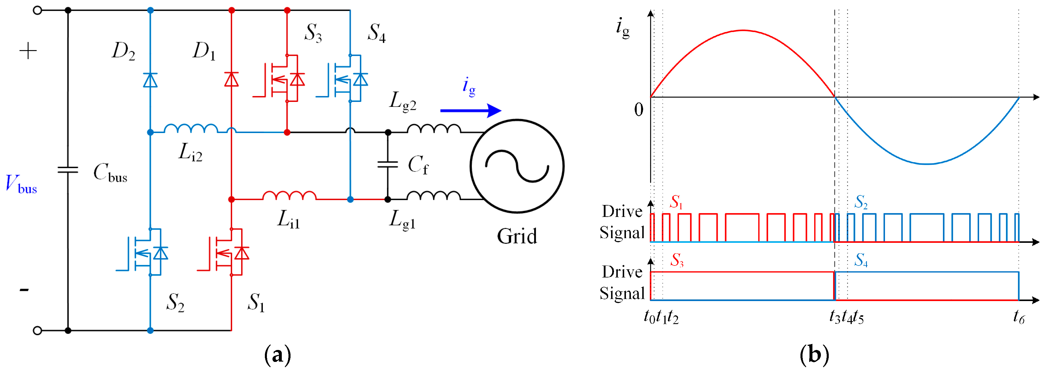
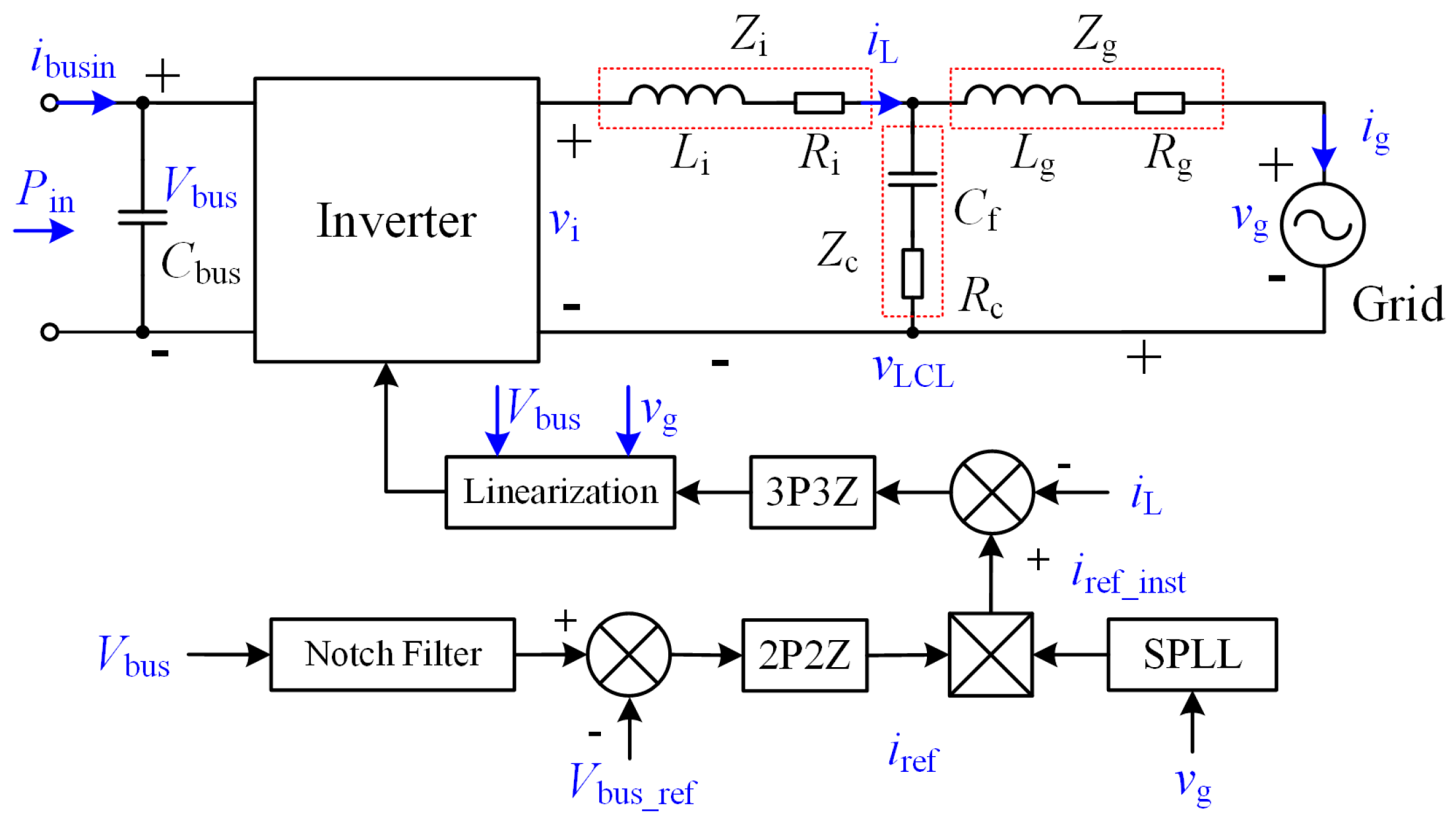
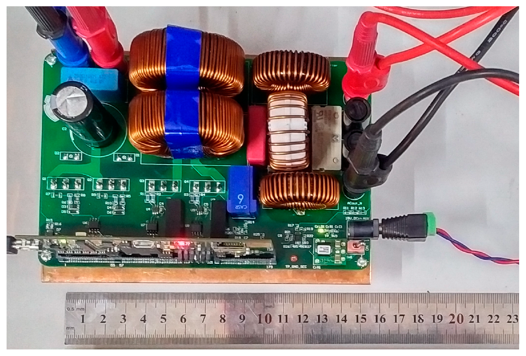
In this paper, a high frequency single phase dual-buck full-bridge grid-connect inverter for small power renewable energy is proposed. The SiC components, as the power devices, are employed to achieve high switching frequency and to limit the conversion loss simultaneously. For the controller, the proposed inverter adopts a current voltage dual-loop. The 3P3Z compensator is adopted in the inner current loop in order to track the current reference which is generated by the 2P2Z compensator. The 2P2Z compensator is employed in the outer voltage loop in order to regulate the DC bus voltage by balancing the input and output power. A systematic way for calculating the losses of high switching frequency inverter is presented. The losses of each component in the inverter are thoroughly analyzed. The switching procedure and the corresponding losses are discussed in detail. The high frequency losses are also taken into account during the analysis. The distribution of the losses is established based on the presented method. Moreover, the deviation between PWM control signal and switching response, which emerges in high frequency switching, is thoroughly analyzed. A designed experiment verifies the influence of deviation. Thus, a compensation method is proposed in order to minimize the influence of deviation. Experiment and simulation confirm the compensation effect. Finally, a 1-kW prototype is made and a 400 kHz switching frequency is achieved. The comparison experiments of the power losses are carried out between Si and SiC power devices to verify the loss calculation method. The results proved the loss analysis is valid.
3. Loss Analysis
The loss analysis is an essential way to improve the system efficiency. For low frequency inverter, the traditional calculation and approximation method are proven to be effective. However, when high speed switching is adopted, the losses, which are overlooked in low frequency condition, may become an indispensable part of the total losses and cause the inaccurate of loss analysis. In this section, the losses of inverter are systematically analyzed. The switching procedure, including the miller effect, is discussed in detail. The high frequency loss is thoroughly analyzed, some of which are not taken into consideration in low frequency applications. Moreover, the loss distribution based on the new method can offer a more accurate and detailed guide line for the improvement of high frequency application.
Before the analysis, several assumptions are made in order to simplify the procedure:
The influence of some parasitic parameters such as leakage inductance is not considered.
The temperature influence on device parameters is not discussed. If the parameter is temperature dependent, the calibration is only based on the datasheet. The analysis is conducted considering the inverter operating temperature is 60 °C.
The parameters of the symmetry components are same and match the datasheet.
The losses of the symmetry components are considered to be the same.
3.1. High Side MOSFET Loss
Basing on operation principles in
Section 2, the high side MOSFETs
S3,
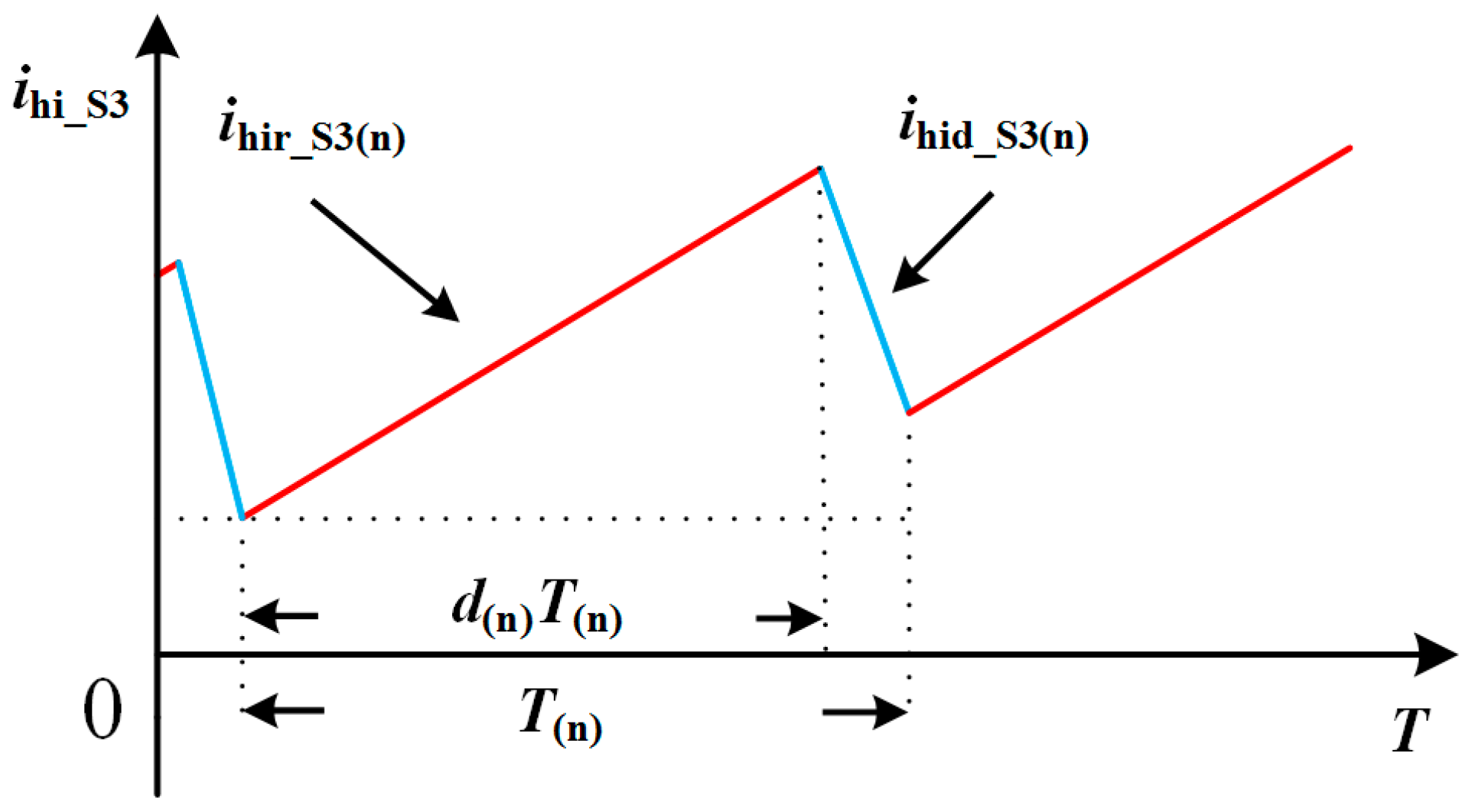
S4 are working at AC frequency. Comparing with the conduction loss, the switching loss can be ignored for their low switching frequency. The D-S current of the high side MOSFET
S3 ihi_S3 is shown in
Figure 3.
When
S3 is turned on, the switching of the low side MOSFET
S1 divides
ihi_S3 into two parts. When
S1 turns on,
ihi_S3 rises,
ihi_S3 flows through
S1, and the current is in rising period; when
S1 turns off,
ihi_S3 falls,
ihi_S3 flows through
D1, and the current is in falling period. The switching of
S1 causes the fluctuation of
ihi_S3.
Tgrid is the gird period.
T(n) is the nth switching period of the low side switch
S1 and the duty cycle is
d(n), the nth conducting time is
d(n)
T(n).
ihir_S3(n) is the
nth rising period of
ihi_S3 which is also the turn-on current of
S1.
ihid_S3(n) is the falling period which is also the free-wheeling current of
D1.
Ns is the number of
S1 switching period which is contained in one AC period. The conduction loss of the high side MOSFET
S3 Phicon_S3 can be divided into two parts:
where
Phircon_S3 is the
ihi_S3 rising period loss and
Phidcon_S3 is the falling period loss,
RDS_S3 is the D-S resistance of
S3 which can be obtained from datasheet.
3.2. Low Side MOSFET Loss
The conduction loss of the low side MOSFET
S1,
Plocon_S1 can be easily deduced from Equation (1). The conduction current is the same as
Phircon_S3 and the only difference is the D-S resistance.
RDS_S1 is the D-S resistance of
S1. Plocon_S1 can be calculated as:
According to the operation principles, low side MOSFETs
S1,
S2 are working at 400 kHz.
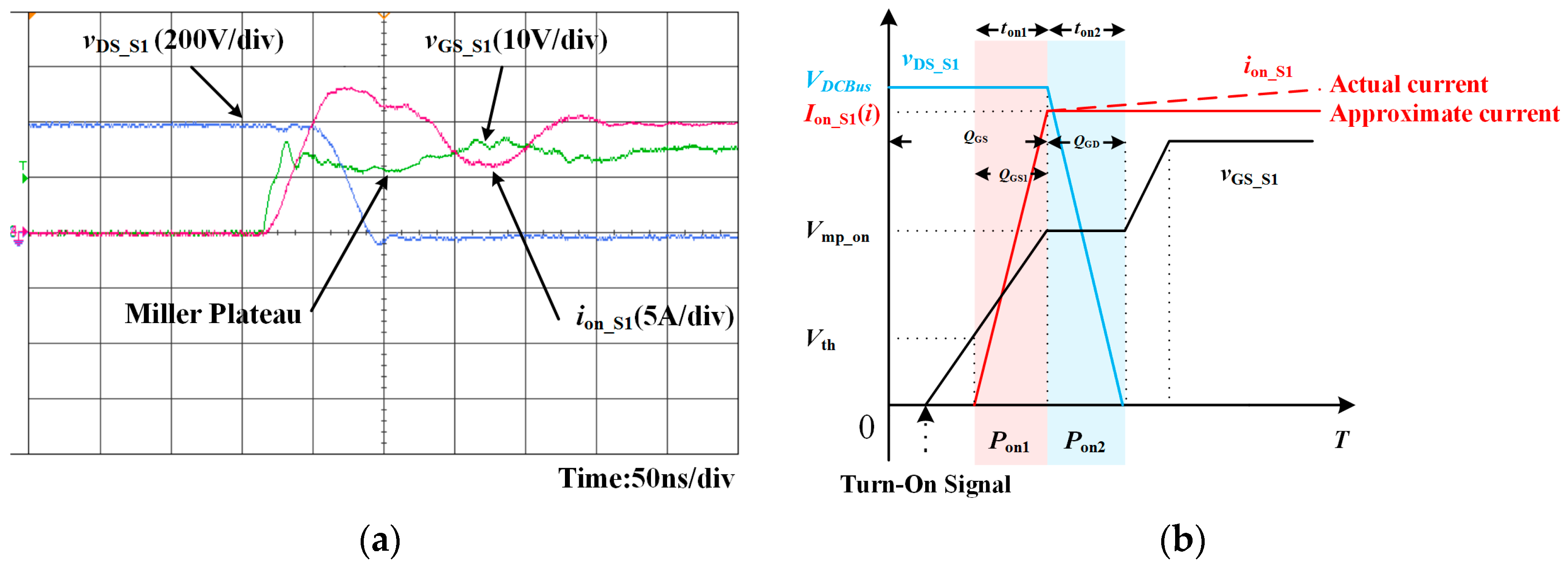
Figure 4a shows the voltage waveforms of
S1 during the turn-on transition and the
Figure 4b is the simplified diagram of the transition.
As
Figure 4b shows, an approximation is made in order to simplify the analysis. The D-S current of
S1 ion_S1 is considered to be a constant current after
ion_S1 is fully turn-on. When a signal starts to turn on
S1, there is a time delay before G-S voltage of
S1 vGS_S1 increases to the gate threshold voltage
Vth. Then, the output capacitance of
S1,
COSS_S1 begins to be charged. The output capacitance loss
POSS_S1 can be calculated as:
where
fSW is the switching frequency of
S1,
VDCBus is the input DC bus voltage and
vDS_S1 is the D-S voltage of
S1. The output capacitance
COSS_S1 is a
vDS_S1 related parameter which is provided by the datasheet.
When
vGS_S1 reaches
Vth, the
ion_S1 starts to rise linearly. After the rising period,
ion_S1 turns on completely, the
vGS_S1 reaches the turn-on miller plateau voltage
Vmp_on and the voltage
vDS_S1 starts to decrease. The miller plateau is caused by the charging or discharging procedure of the capacitance between G-D, which is
CGD [
20]. In actual waveform, as
Figure 4a shows, miller plateau have a slope. The steepness of the slope is depending on the value of
CGD and
CGS, where
CGS is the capacitance between G-S. Typically,
CGD is larger than
CGS, the phenomenon appears as a plateau. The duration time can be considered as the charging time to charge
QGD, which is the gate to drain charge.
At the end of the miller plateau, the
vGS_S1 reduces to zero and the turn-on procedure is completed. During the turn-on transition, the turn-on loss
Pon can be divided into two parts:
Pon1 and
Pon2. The
vGS_S1 is constant and
iS1 is linearly changed during
ton1. Similarly, the
iS1 is constant and
vGS_S1 is linearly changed within
ton2. The turn-on loss of
S1 Pon_S1 can be deduced form Equation (6).
where
Ion_S1(n) is the nth switching period turn-on current of
S1.
QGS2 represents the corresponding charge during
ton1 which can be calculated according to the transfer characteristic figure of devices,
RGon is the gate loop resistance during turn-on period.
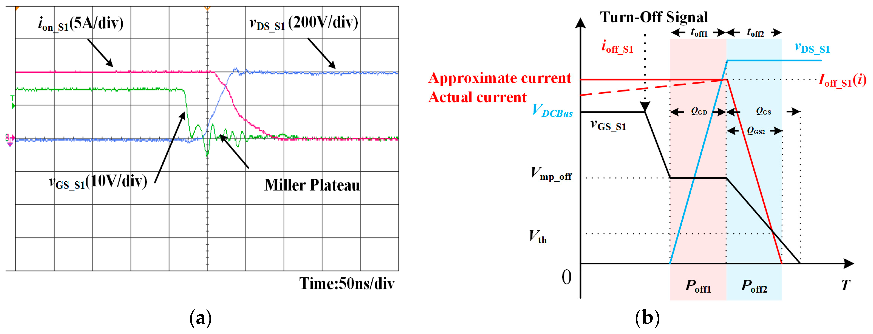
Figure 5a shows the waveforms of
S1 during the turn-off transition and the
Figure 5b is the simplified diagram of the transition. A similar approximation is made which considers the D-S turn-off current of
S1 ioff_S1 to be constant before
toff2. When the signal starts to turn off
S1,
vGS_S1 starts to decrease. The
vGS_S1 begins to increases when
vGS_S1 reaches the turn-off miller plateau voltage
Vmp_off. At the end of the plateau,
vGS_S1 stops increasing and
ioff_S1 starts to decrease. The turn-off transition is completed when
vGS_S1 goes down to
Vth and
ioff_S1 decreases to zero. The turn-off loss
Poff_S1 can be regarded as two parts:
Poff1 during
toff1 and
Poff2 during
toff2 which can be calculated by Equation (7).
where
Ioff_S1(n) is the nth switching period turn-off current of
S1.
RGoff is the gate loop resistance during turn-off period. The total loss of
S1 Ploss_S1 is regarded as:
3.3. Free-Wheeling Diode Loss
The conduction loss of the free-wheeling diode
D1,
Pdcon_D1 can be deduced from Equation (2), which is shown in Equation (9):
Uf is the forward voltage of the diode. The turn-on loss of the diode
Pond_D1 can be represented as (10):
where
Ud is the voltage on the diode.
Idon(n) is the nth diode turn-on current which can be approximated as the
(n − 1
)th turn-off current of
S1 Ioff_S1(n−1).
tr is the rising time of the
S1 which can be approximated as
ton1.The turn-on loss of the diode
Poffd_D1 can be represented as (11):
IRM is the diode peak reverse current and trr is the reverse recovery time.
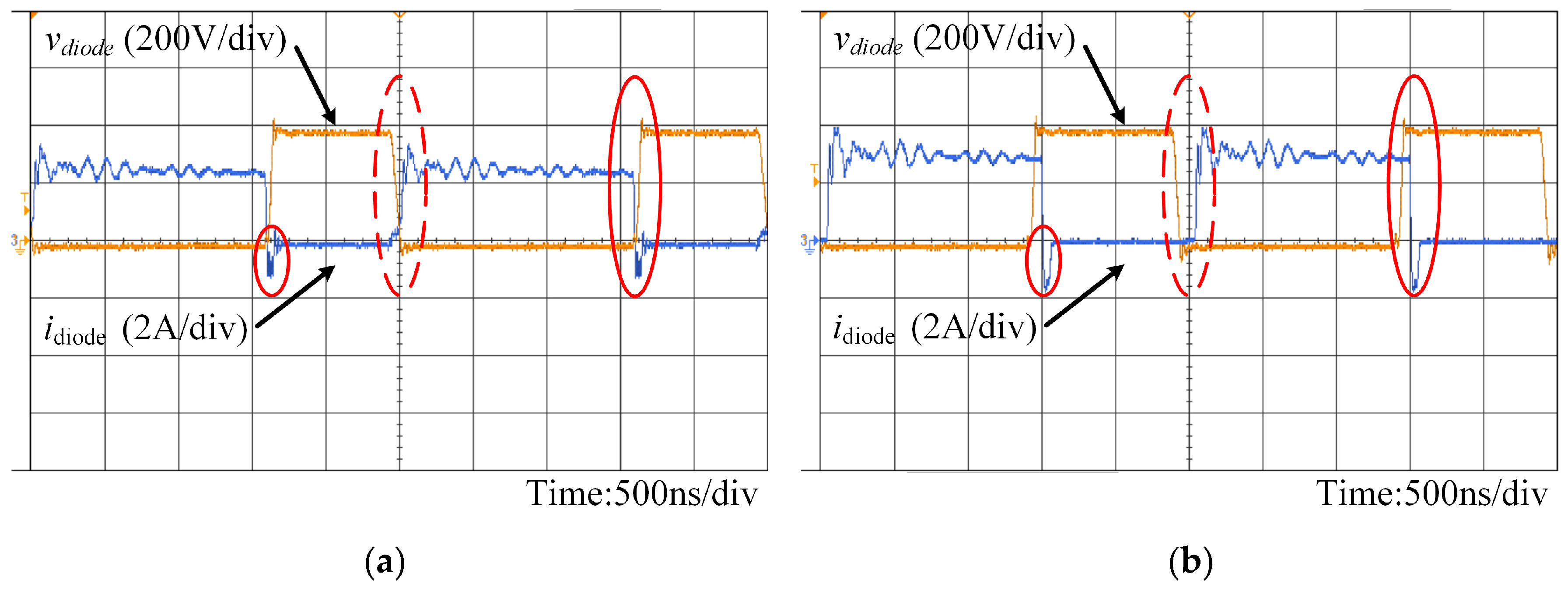
3.4. Inductor Loss
The copper loss
PLCu of filter inductor can be calculated as
where
iL is the inductor current and the
RL is the resistance of the inductor winding.
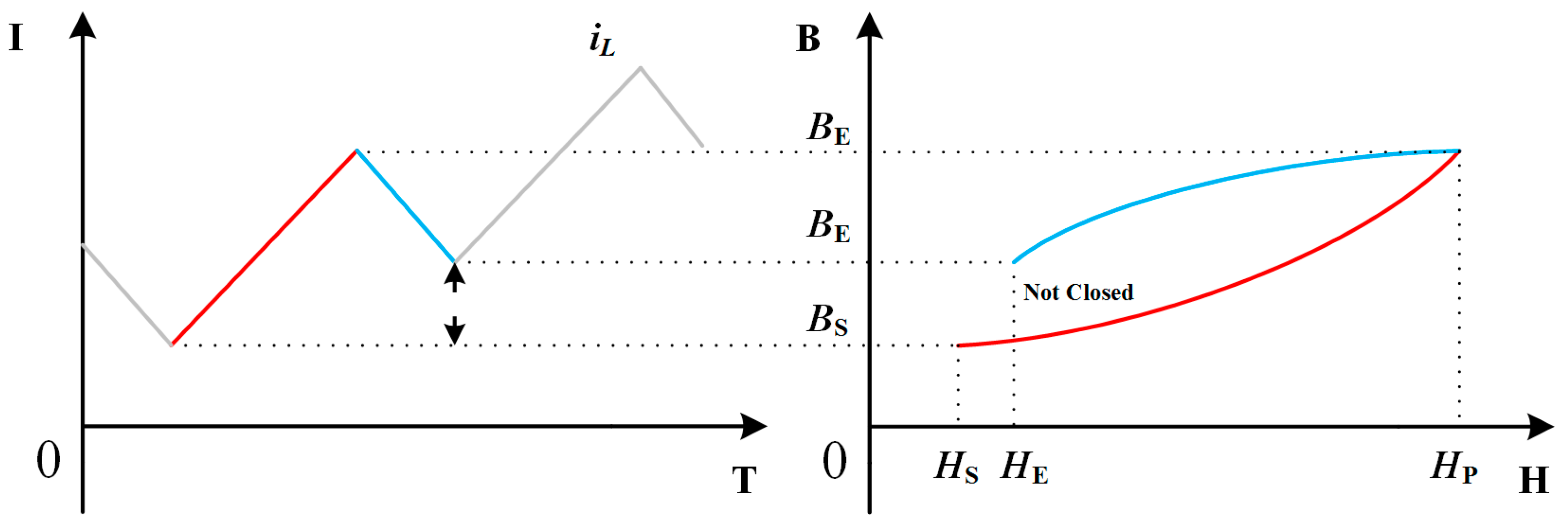
Figure 6 shows the trajectory of inductor current
iL on the B-H plane during one switching cycle. At the end of the switching cycle, the
iL is not the same as the initial value because the inverter is working in continuous current mode in order to follow the sinusoidal reference. The work mode leads to the unclosed B-H curve as
Figure 6 shows. Accordingly, the traditional hysteresis loss calculation based on closed B-H curve is not suitable for inverter hysteresis loss calculation. The unclosed B-H curve should be adopted [
21,
22,
23].
Magnetic flux density
B can be obtained by integral of the inductor voltage
uL. The magnetic flux density at
tn can be calculated as:
where
N is the number of winding turns and
A is the cross-section area of the inductor core.
iL(
tn) is the inductor current at
tn, the magnetic field intensity
H(
t1) can be obtained by:
where
l is the length of the equivalent magnetic circuit. The hysteresis loss
Physis can be calculated as:
3.5. Capacitor Loss
The loss which is caused by the leakage current of the capacitor
Pcleak can be calculated as:
Uc is the voltage on the capacitor, and Icleak is the leakage current of the capacitor, which is a Uc related parameter and can be found in the datasheet.
Rcs is the resistance of the capacitor lead and electrode,
Irip is the ripple current of the capacitor, and the loss on these conductors can be represented as:
RESR is the equivalent series resistance of the capacitor, which can be deduced form dissipation factor tan
δ:
where
f is the frequency which the ESR is calculated at.
C is the capacitance of the capacitor. The ESR loss of the capacitor can be calculated as:
The total losses on the capacitor is
3.6. Loss Calculation Results
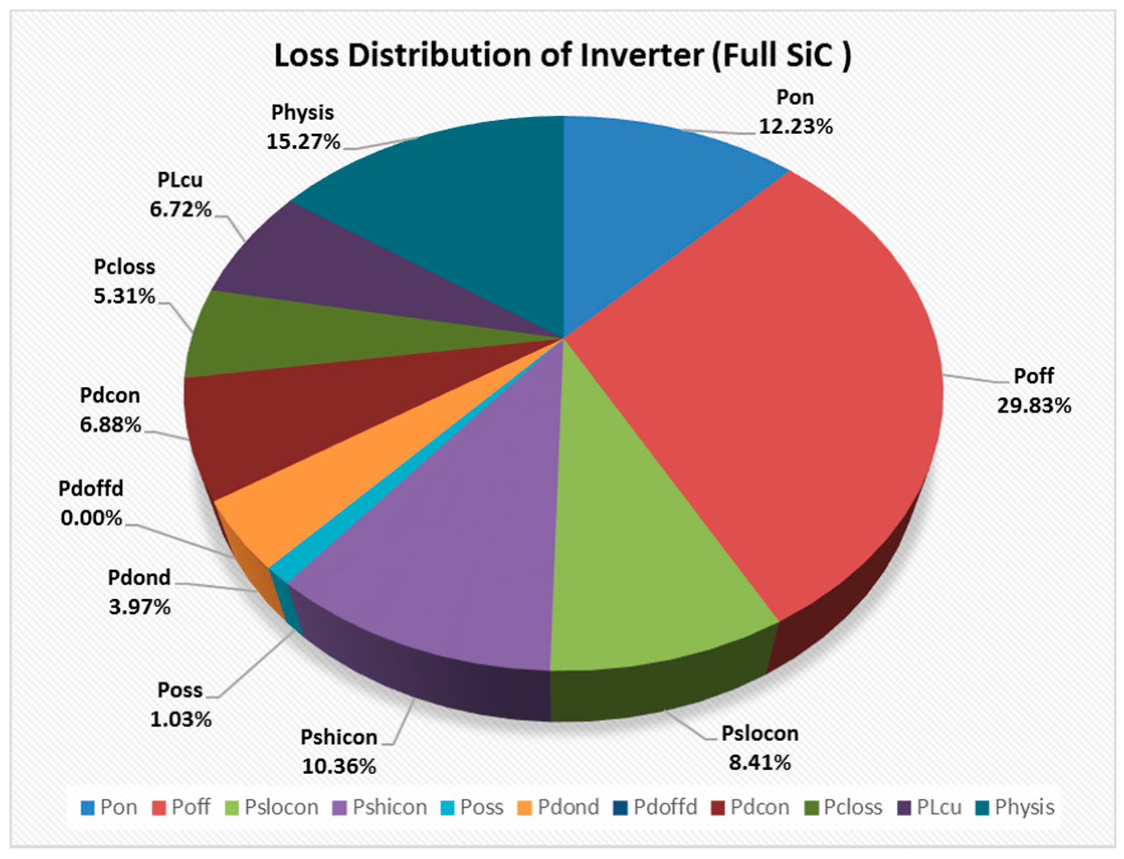
Based on the previous methods, the calculation results of the Full SiC power devices inverter losses are shown in
Figure 7 as calculation Example 1.
As we can see from
Figure 7, the switching loss takes the major part of the total loss. The output capacitance loss
POSS, which is often overlooked in low frequency loss analysis, is over 1% and should be taken account in high frequency application. For the special characteristic of the SiC diode, the reverse recovery time
trr is consider to be 0. Hence, the free-wheeling diode turn-off loss
Pdoff is 0. This superiority, which is proven in later experiment, is vital for the total loss of the inverter. Finally, the calculation efficiency is 97.32% at rated power of 1 kW.
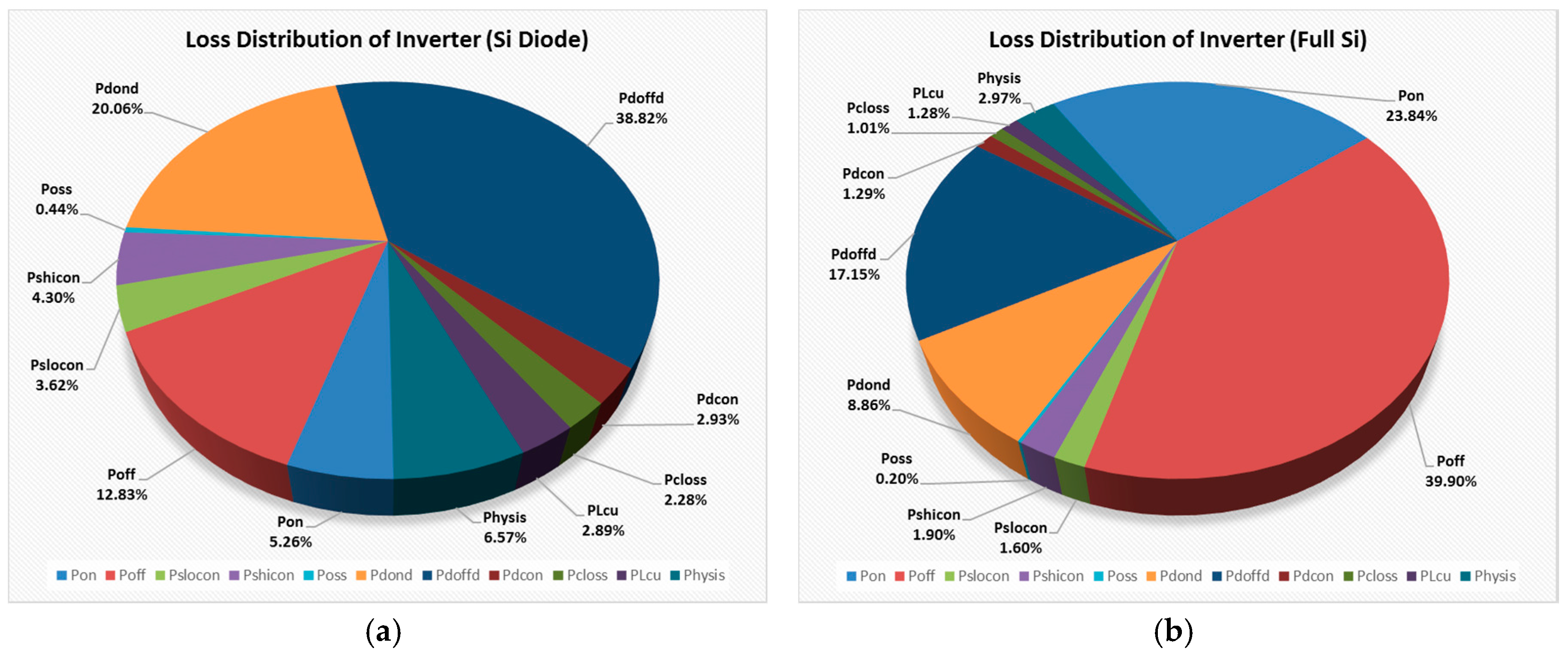
Two comparative calculation examples are set up. In Example 2, the free-wheeling diodes
D1,
D2 are replaced by two normal Si diodes. In Example 3, all the power devices are replaced by the normal Si devices. The loss distribution of the comparative calculation examples are shown in
Figure 8.
As
Figure 8a shows, when the SiC diodes are replace by the normal Si diodes, the total loss on the diodes is over 50%. The turn-on loss and the turn-off loss of the diodes contribute the most part of the losses increase. As a result, the calculation efficiency of Example 2 is down to 93.57% at 1 kW.
After all the power devices are replaced by the Si devices. The losses of the switches become the major part of the total losses. Consequently, as
Figure 8 shows, the total loss of Example 3 is almost three times larger than Example 2. The calculation efficiency of Example 3 is 85.27% at 1 kW.
The total loss comparison is shown in
Figure 9. For Example 2, the diode losses contribute the most. For Example 3, the losses on the switches are numerous. The total losses difference between the Full SiC and Full Si power device is over five times. These results are confirmed in later comparative experiments, which indicate that the Si power devices are not suitable for high frequency application.
4. Improved Simulation Method
A simulation model is often built in software environment in order to verify the validity of theoretical analyses and accelerate the compensator tuning. In low frequency converting, the simplified component models are considered to be effective and timesaving. However, as the switching frequency increases, some details of the switching procedure may have a serious influence on the simulation, which could make the results become inaccurate, even unreliable. The inconsistency between the simulation results and experiment results emerges during the design process. The deviation between PWM control signal and switching response in high frequency switching is consider to be the reason which cause the inconsistency. The influence of the deviation on the simulation is verified by experiment. Moreover, based on the theoretical analysis and test results, a compensator method is proposed in order to minimize the deviation which is caused by the influence. Consequently, the simulation results are significantly improved. The improved simulation model is used in prototype design to verify the compensators. The method is proven to be effective by the experiments in later section.
4.1. Influence of High Frequency Switching
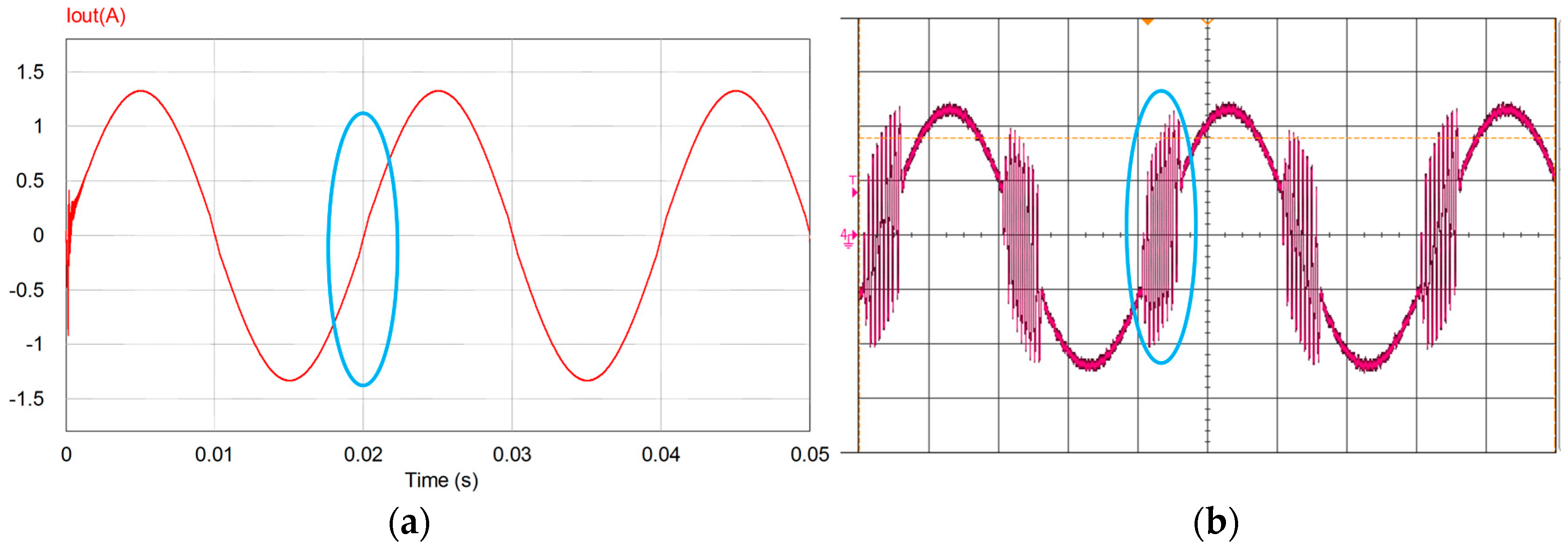
A simulation model is built in software environment of PSIM. The parameters of the components and control compensator are the same as the experimental prototype. The grid-connecting power experiments are carried out. The 3P3Z compensator in the current loop, which is designed to follow the current reference, are tuned and tested on the simulation model. As
Figure 10a shows, the compensation effect is desirable. However, during the experiment, the same compensator, which has the same parameters, causes the current oscillation during zero-crossing procedure.
The same simulation method is used in the previous 50 kHz inverter design and no similar issue arises. Through analysis, the deviation between PWM control signal and switching response in high frequency switching, is the main reason which causes the simulation to be inaccurate.
4.2. Equivalent Opening Time
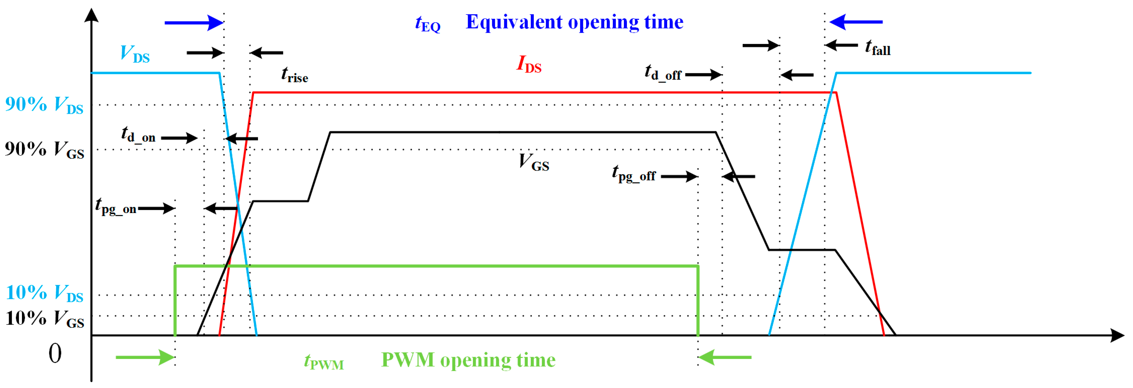
Figure 11 shows the waveforms of a complete switching cycle. The PWM signal is considered to be an ideal square wave. When the rising edge of the PWM signal begins to turn on the switch, there is a turn-on propagation delay
tpg_on before the G-S voltage starts to rise. The delay is caused by the drive circuits when converting the PWM signal into drive signal. When
VGS rises, the D-S voltage
VDS starts to descend. The time, which is from 10%
VGS to 90%
VDS, is defined as the turn-on delay
td_on. The time, which is form 90%
VDS to 10%
VDS, is the rise time
trise. The turn-off propagation delay
tpg_off, turn-off delay
tdoff and fall time
tfall can be obtained by similar definitions. The equivalent opening time is define as the period which the
VDS fall below 90% then rise over 90%. As
Figure 11 shows, the relationship between PWM opening time
tPMW and the equivalent opening time
tEQ can be represented as Eqaution (21)
The equivalent opening time
tEQ can be regarded as the actual respond of the switch under the control of PWM signal. In practical circuits,
tpg_on and
tpg_off are small and assumed to be equal. Hence, Equation (21) can be simplified as:
where
te is the total extend time which is caused by the delay in the switching procedure.
td_on,
td_off,
tfall and
trise are all
VDS related parameters provided by the datasheet. It is obvious that the PWM opening time is extended during the switching procedure. The proportions of the deviation in the equivalent opening time
tEQ under different switching frequencies and duty cycles are shown in
Table 1.
As
Table 1 shows, when the switching frequency is low, the proportion of
te in
tEQ is very small. During the practical circuit design, this deviation is often ignored. However, in high frequency implementation, this time deviation may even larger than
tPWM. When the
fsw is at 400 kHz, at 2% duty cycle, the proportion of
te is over 50%.
tPWM is extended about two times. This deviation may lead to the inconsistency between the output and control signal. This difference has an error accumulation effect, which can cause the error response of the controller. As a result, the compensator, which is tested in the simulation and consider to be valid, will fail on the prototype.
In order to verify the analysis, an off-grid DC experiment is set up, for the deviation is more obvious when the duty cycle is constant. The difference between the output currents can prove the pervious analysis. The prototype connects to a 100 Ω resistor instead of the gird, then runs at 50 kHz and 400 kHz respectively. A constant duty cycle is given to the inverter in order to run the inverter in DC output mode. The output current
itest is tested at each duty cycle at different switching frequency. Meanwhile, the same test is carried out on the simulation model. As
Figure 12 shows, the output current at the same duty cycle of simulation and experiment are represented by two respective curves. There is almost no difference between the experiment results and simulation results when the switching frequency is at 50 kHz as
Figure 12a shows. Because the proportion of the deviation in low frequency is very small, which can be ignored in traditional analysis. However, when the switching frequency is at 400 kHz as
Figure 12b shows, there are significant differences between the simulation results and the experiment results. When the test duty cycle is under 45%, the experiment output current is apparently larger than the simulation results at the same duty cycle. This phenomenon can be explained as the control PWM signal in the prototype is extended by the delays which we talked above. The phenomenon is more obvious at low duty cycle which is consistent with previous analysis.
4.3. Compensating Method
Different from other researches, the proposed method focuses on the impact of the switching procedure on the output power. Instead of simulating the complex switching procedure in detail, a compensating module is used to improve the simulation results. The proposed method is simple and effective. Based on Equation (22),
dEQ is the duty cycle based on
tEQ and can be calculated as:
where
tsw is the switching period, and
dPWM is the duty cycle of the input PWM. The compensator is added between the Linearization module and PWM generating module (
Figure 13).
The linearization module [
24,
25,
26] is used to generate the duty cycle
dPWM for controlling the switches. The duty cycle
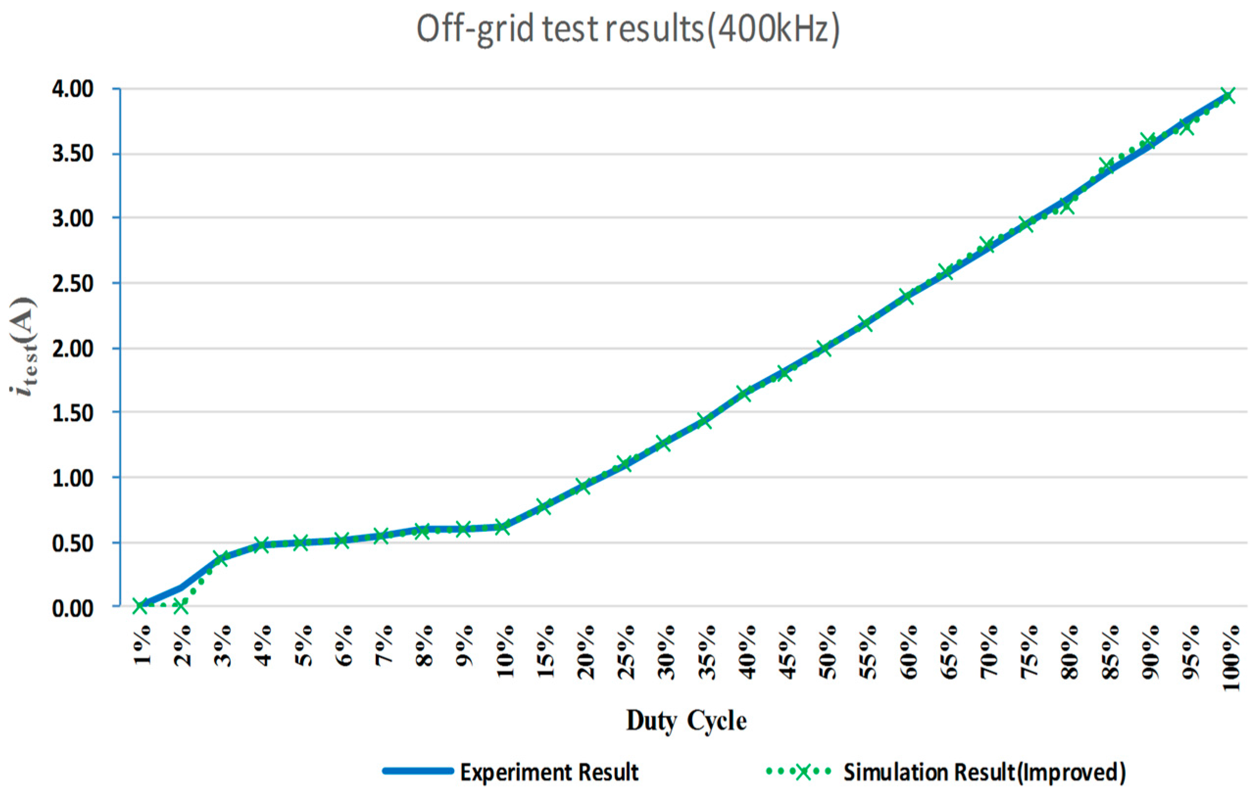
dPWM is compensated by the duty cycle compensator. In order to test the compensation effect, the 400 kHz off-grid DC experiment is carried out on the improved simulation model. The simulation results are shown in
Figure 14. Apparently, the compensator module is able to simulate the prototype output current correctly. The deviation of the output current between the simulation and experiment is minimized successfully.
Because of the deviation, the characteristic of compensator at low duty cycle have to be adjusted. Based on the improved simulation model, the characteristic of the inverter is re-analyzed. The compensator is redesign accordingly. The oscillation during zero-crossing is restrained by the new compensator in the simulation. The compensation effect is proven by the further experiment. The output waveforms of the experiments are shown in the later section.
