Article

Control of Current Phase Advancing in Single-Leg Power Converters with the Use of Switched Capacitors

by
Roman Konarik
*,†,‡,
Jozef Sedo
†,‡,
Branislav Dobrucky
†,‡ and
Michal Prazenica
†,‡
Department of Mechatronics and Electronics, Faculty of Electrical Engineering, University of Zilina, 010 26 Zilina, Slovakia
*
Author to whom correspondence should be addressed.
Current Address: Department of Mechatronics and Electronics, University of Zilina, Univerzitna 8215/1, 010 26 Zilina, Slovakia.
These authors contributed equally to this work.
Energies 2018, 11(10), 2761; https://doi.org/10.3390/en11102761
Submission received: 11 September 2018 / Revised: 9 October 2018 / Accepted: 10 October 2018 / Published: 15 October 2018

Abstract

:
This paper deals with the control of current phase advancing in single-leg voltage source inverters (VSI) and matrix converters with a two-phase output. The phase shift of the current in the auxiliary phase is set with the use of switched capacitors. Two distinctive control methods are used for the current phase advancing, open-loop control and closed-loop control. In addition, a new averaging method is derived for the calculation of the switched capacitance used in the open-loop control. The practical use of the designed control methods with the switched capacitor is shown in simulations and experimental verifications on a single-leg matrix converter with a passive and active load (induction motor).

1. Introduction

A topology of the single-leg matrix converter (MxC) is derived from a single-leg VSI converter system with input rectifier [1,2,3]. The analysis of such a MxC topology scheme has been done [4,5]. The advantages of those schematics are presented by the absence of the input rectifier and bulky filtering capacitor and consequently higher efficiency. This is possible by switching of both reversible connected switches (metal-oxide-semiconductor field-effect transistors ), [6]. Using switched capacitors for creating of quadrature supply or two/phase induction motor fed by VSI converter is described in [7]. For IM fed by single-leg MxC, please refer to the following works [8,9].
The use of switched capacitors has been previously published for VSI supply systems in [10,11,12], for single-leg VSI in [7], and for single-phase VSI in [7,11]. All these applications with switched capacitors are derived for steady state with real-time closed-loop control. The use of switched capacitor control for single-leg VSI has not yet been published. For a single-leg matrix converter, the use of switched capacitors is described in the authors’ recent work [8,9].
These MxC or VSI converters require controlling the capacitance due to the single-leg output of the converter when using two-phase passive or active loads. The auxiliary phase is connected in series with switched capacitors to the converter output in comparison to the main phase which is connected directly to converter output. Multiple topologies of switched capacitors exist with different configurations of switches and capacitors with different properties.
This paper deals with phase shift control of current in a single-leg matrix converter with a two-phase output. A known topology of two parallel connected capacitors and switches is used. Two different control methods are used for the current phase advancing. The first method uses open-loop control, where the required 90 degrees phase shift between the current in the main and auxiliary phase is calculated based on the parameters of the load (resistance and inductance). A novel method for control of the desired variable switched capacitance is also derived for the use in the open-loop control. The closed-loop control of current phase shift is inspired by the phase-locked loop.

2. Principle of Operation

The switched capacitors are comprised of one large capacitor and one small capacitor and two switches (Figure 1a). During the operation, only one switch is in the on-state at a time. A single-pole-double-throw switch is used in our analysis and modeling of the switched capacitors (Figure 1b).
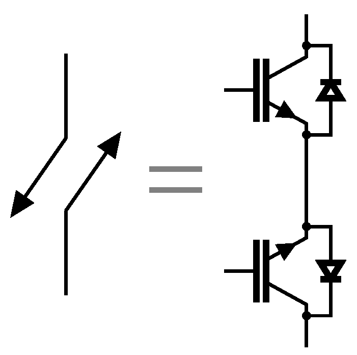
The switch needs to be able to block the voltage of both polarities and conduct the current in both directions. One of this type of switch, two anti-series emitter connected insulated-gate bipolar transistors (IGBT), with the equivalent symbol used in this paper, is shown in Figure 2.

2.1. Method of Conservation of Energy

From the potential energy stored in the capacitors can be deduced the equation for the controlled switched capacitance [7]. The capacitors potential energy is
E = 1 2 C v 2 ,
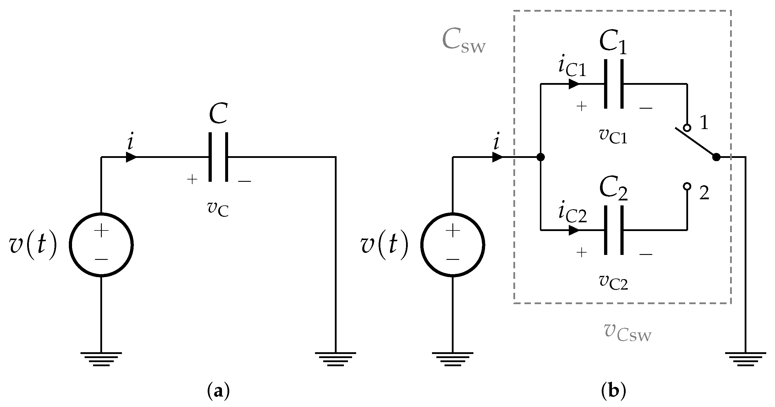
where E is the energy stored in the capacitor, C is the capacitance, and v the voltage of the capacitor. The schematic in Figure 3a shows the voltage source connected with the capacitor.
The average voltages on the capacitors are
v C 1 = D V , v C 2 = ( 1 D ) V ,
where D is the duty cycle, V is the constant voltage on the voltage source, and v C 1 and v C 2 are the average voltages on the capacitors.
Then, the total energy stored in the two capacitors is
E = E 1 + E 2 .
Combining Equations (1)–(3) yields the value of the switched capacitance as
C SW = C 1 D 2 + C 2 ( 1 D ) 2 .
The equivalent switched capacitance C SW with voltage source is shown in Figure 3b. The capacitance C SW needs to equal C.
From Equation (4), the value of duty cycle can be derived as
D = C 2 ± C SW C 1 + C 2 C 1 C 2 C 1 + C 2 .

2.2. Averaging Method

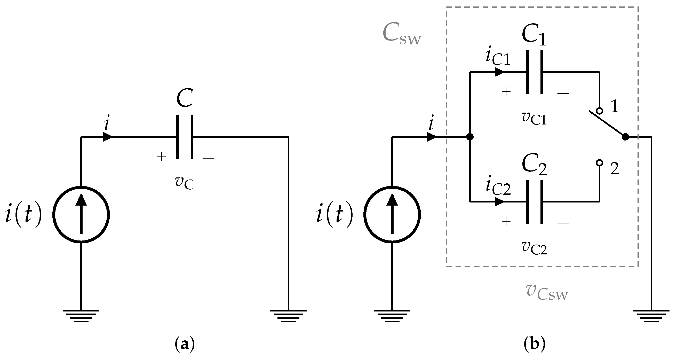
We now use a current source as shown in Figure 4 [9,13]. The voltage on capacitor is given as
v C t = 1 C i t d t ,
where i ( t ) is the current in the capacitor C. We can consider the capacitor current as constant values at sufficient high switching frequency i ( t ) = I .
In the first interval, as shown in Figure 4b, the average current flowing in the capacitor C 1 is given as
i C 1 = D I ,
where I is the value of a constant current source. During the second interval, the average current on the capacitor C 2 is given as
i C 2 = ( 1 D ) I .
We can now derive the voltages on the capacitors C 1 and C 2 from Equations (6)–(8) as
v C 1 t = 1 C 1 D I t ,
v C 2 t = 1 C 2 1 D I t ,
where t is time. We can look at the capacitor voltages as constant values at sufficient high switching frequency v C 1 t = V C 1 , v C 2 t = V C 2 .
The average voltage during one switching period from capacitor C 1 is
v C 1 = D V C 1 ,
and from the capacitor C 2
v C 2 = ( 1 D ) V C 2 .
The average voltage on the switched capacitor is then
v C sw = D V C 1 + ( 1 D ) V C 2 .
The voltage on the single capacitor C needs to equal the voltage on the switched capacitor C SW
v C t = v C sw t ,
which is equal to the average voltage
v C t = v C sw .
Voltage on the capacitor C is given as
v C t = 1 C I t .
Substituting Equations (9), (10), (13) and (16) into Equation (15) yields
1 C SW = 1 C 1 D 2 + 1 C 2 ( 1 D ) 2
The duty cycle can be calculated from Equation (17) as
D = C 1 + C 1 C 2 2 4 C 2 2 4 C 1 + 4 C 2 1 C 2 1 C SW C 1 + C 2 .
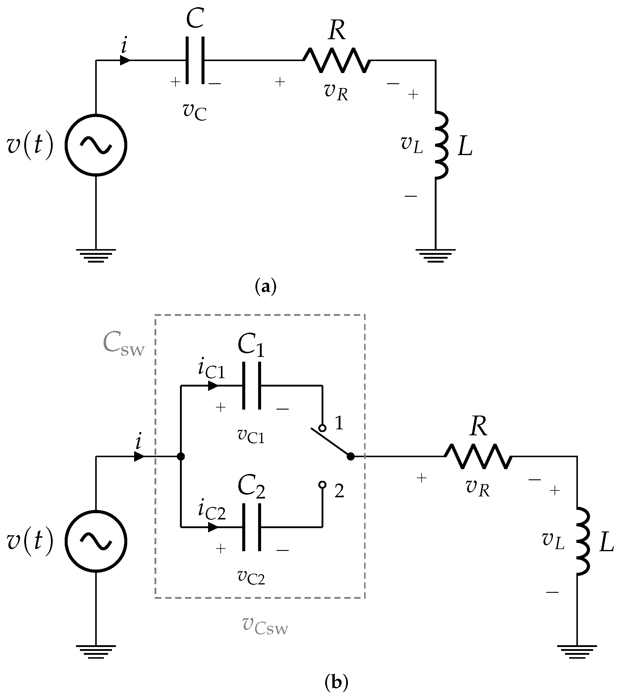
Let us now look at Figure 5, where we have an RL load connected in series with the capacitor and a harmonic voltage source. The differential equation, describing the RLC circuit in Figure 5a, is
v t = R i t + L d i t d t + v C t ,
and in the integrodifferential form as
v t = R i t + L d i t d t + 1 C i t d t .
A similar equation applies for the circuit with the switched capacitor in Figure 5b.
v t = R i t + L d i t d t + v C sw ,
where the voltage v C ( t ) equals v C sw , when we neglect the switching ripple. The capacitors C 1 and C 2 voltages are substituted into Equation (21) as
v t = R i t + L d i t d t + D v C 1 t + 1 D v C 2 t .
Using Equations (9) and (10), we get the integrodifferential equation as
v t = R i t + L d i t d t + D 2 C 1 i t d t + ( 1 D ) 2 C 2 i t d t = R i t + L d i t d t + D 2 C 1 + ( 1 D ) 2 C 2 i t d t .
Substituting Equation (17) into Equation (23) yields
v t = R i t + L d i t d t + 1 C SW i t d t .
Equation (24) (Figure 5b) with switched capacitors is equivalent to Equation (20) (Figure 5a) with a single capacitor. The average value of the capacitance C SW in the switching capacitors is the same as the value of capacitance C in a single capacitor.
The current i stays almost constant thanks to the inductance L for one switching period. The switching frequency is much larger than the frequency of the harmonic voltage source f s f , and therefore the current i can be expressed as constant. Because of this, we can use the derived equations also with RLC circuit and a harmonic voltage source.

2.3. Comparison of the Methods

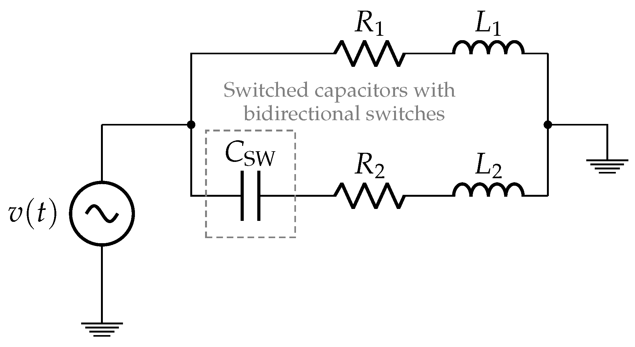
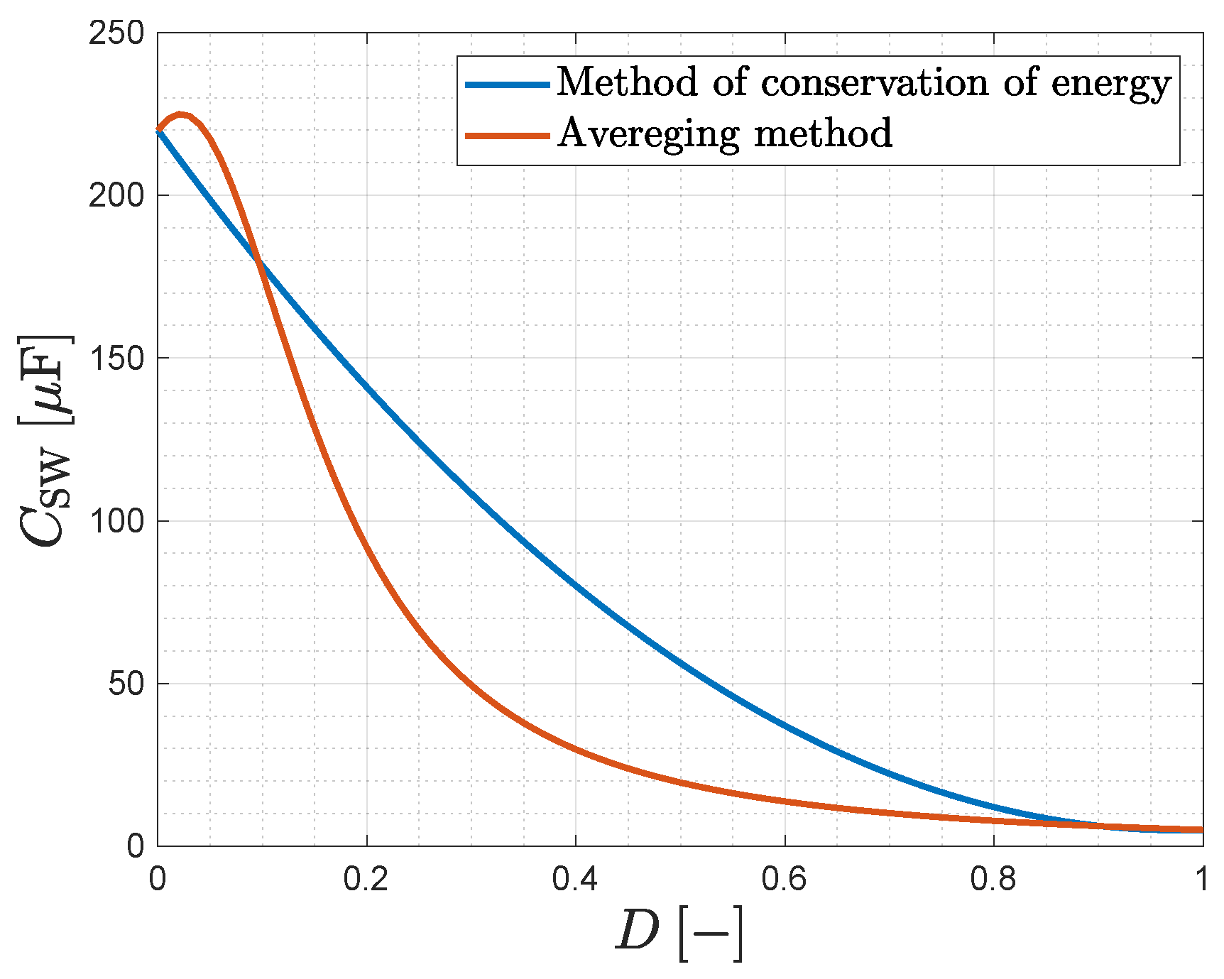
The circuit in Figure 6 was simulated in MATLAB/Simulink (R2018a, MathWorks, Natick, MA, USA) environment with the following parameters: R 1 = 70.53 Ω , R 2 = 52.9 Ω , L 1 = 170 mH , L 1 = 120 mH , C 1 = 5 μ F and C 2 = 220 μ F . The calculated value for the capacitor is C SW = 33.867 μ F for the frequency f = 40 Hz .
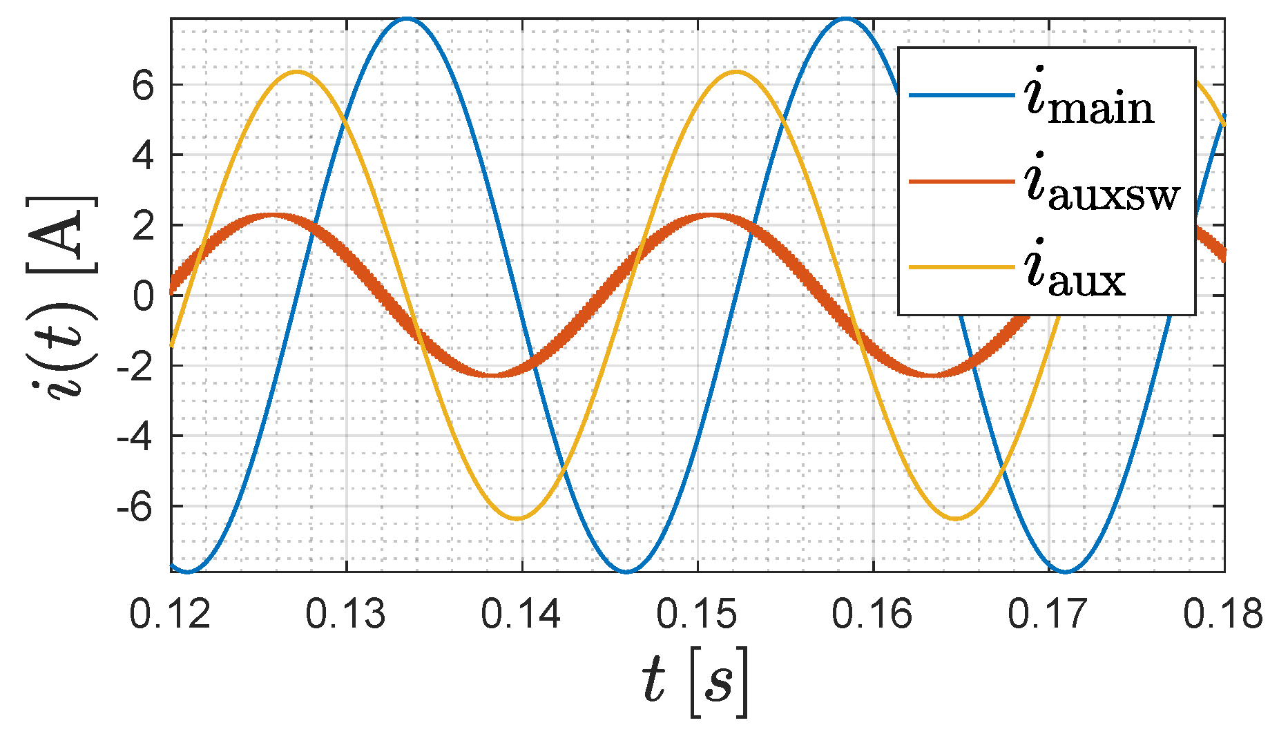
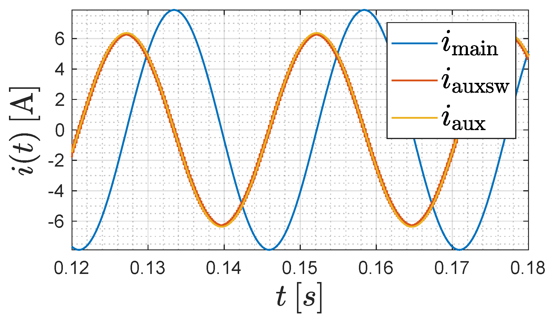
The first simulation results, shown in Figure 7, were gained using the method of conservation of energy. The simulation shown in Figure 8 was conducted using the averaging method. The calculation of the capacitance needed for the phase shift is described in the next section. The variables in the figures are as follows: i main is the current in the main phase, i aux is the current in the auxiliary phase with a normal capacitor (Figure 5a) and i auxsw is the current in auxiliary phase with switched capacitors (Figure 5b).
As we can see, the first method does not have an exact phase shift of 90 degrees between the two currents. On the other hand, the second method has an exact phase shift of 90 degrees.
The current in auxiliary phase with a single capacitor matches the current with switched capacitors.
The difference in the value of the set (calculated) capacitance can be seen in Figure 9. The current i does not charge the capacitors C 1 and C 2 to the same voltage value and this is the reason the first method fails, as it assumes the same voltage on both capacitors.

3. Control of Phase Advancing with Switched Capacitors

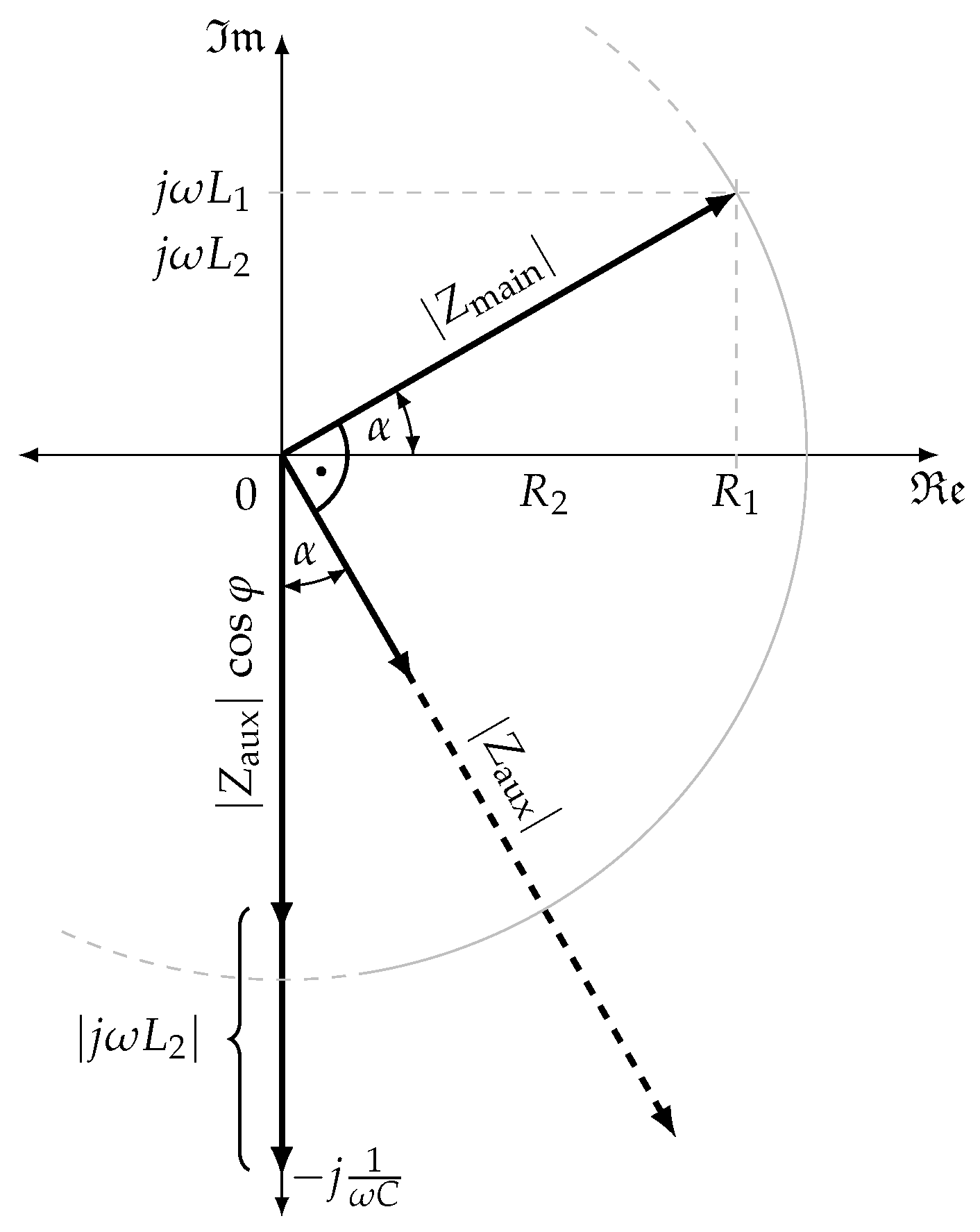
The equations for the switched capacitors are now used to control the phase shift of the current. Figure 6 shows a harmonic voltage source with two-phase RL load (main phase R 1 L 1 and auxiliary phase R 2 L 2 ) and a switched capacitor connected in series with the auxiliary phase. During the change of frequency, the phase shift is always constant at 90 degrees. The following equations describe the calculation of the capacitance
α = arctan ω L 1 R 1 ,
where ω is the angular frequency.
Z aux = R 2 sin α ,
where Z aux is the impedance of the auxiliary phase.
The value of the capacitance is then calculated as
C = 1 ω ( Z aux cos α + ω L 2 ) .
The calculation of the capacitance for 90 degrees phase shift is also shown in the vector diagram in Figure 10.
For a variable phase shift, as shown in Figure 11, the following equation can be used for the calculation of capacitance
β = φ α ,
γ = { π 2 β , β > 0 β , β < 0 ,
C = { 1 ω ( Z aux cos γ + ω L 2 ) , β > 0 1 ω ( Z aux sin γ + ω L 2 ) , β < 0 1 ω 2 L 2 , β = 0 .

3.1. Open Loop Control

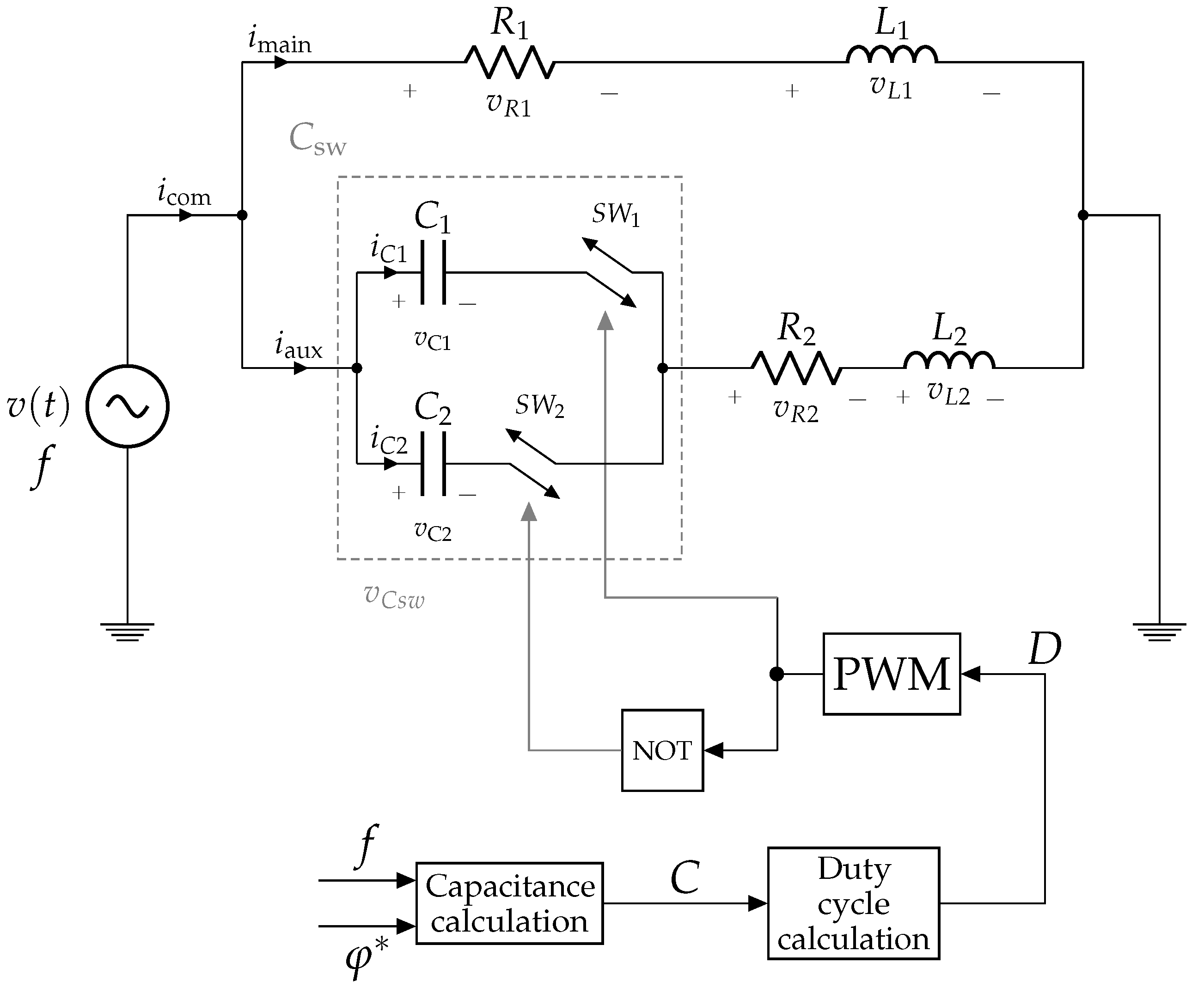
In open-loop control, the 90-degree phase shift is calculated from precise values of the system parameters (frequency, inductance, and resistance) [9]. We can see the open-loop scheme and simplified control diagram in Figure 12 and Figure 13. First, the value of the capacitance is calculated based on these parameters. Second, the value of the duty cycle which controls the value of the switched capacitor is calculated based on the required capacitance and the values of the capacitors that are switched. These methods were described in previous chapters. The advantage is that there are no stability issues as in a feedback loop, and also no dynamics response of the control output (duty cycle). The disadvantage is that we need to know the parameters of the system, and, if the parameters of the system (inductance and resistance) change over time, the phase shift will also change from the set value of 90 degrees. The method of open-loop control is used in Section 2.3.

3.2. Closed-Loop Control

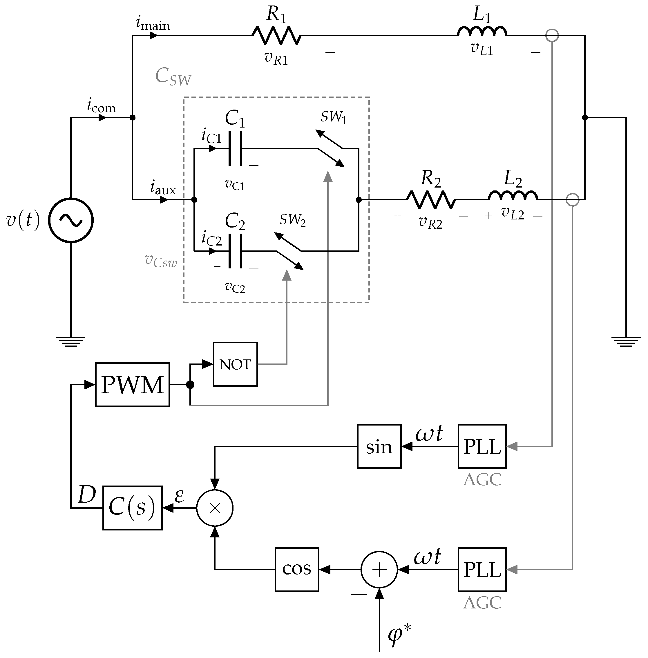
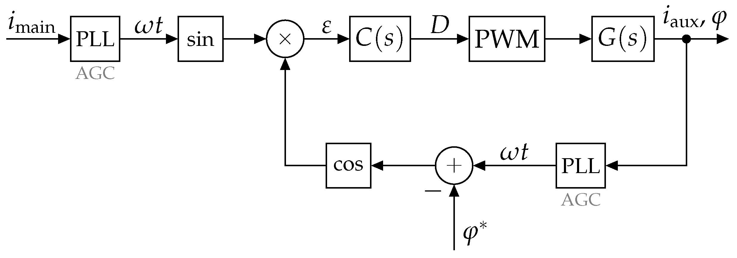
The closed-loop (feedback) control [14] of the phase shift was inspired by an analog phase-locked loop PLL [15]. We can see the complete control scheme with the circuit in Figure 14. The simplified block diagram is shown in Figure 15. Similar to a PPL, we also require a phase detector to compare the phase shift between main and auxiliary phase currents. A simple mixer (multiplication) is used as the phase detector to compare the phase signals. The current signals in the main and auxiliary phase have different magnitudes. This, however, would also affect the phase detector output, and we want to compare only the phase shift. To solve this problem, two PLLs with automatic gain control AGC are used for measurement of the current signals. The PLLs have unity magnitude outputs thanks to AGC. Another benefit of the PLLs is the removal of noise and current ripple from the signal.

3.2.1. Linearization of the Phase Detector

The large signal phase detector output in Figure 15 can be written as follows
ϕ e = sin ( ω t + ϕ main ) cos ( ω t + ϕ aux φ * ) = sin ( ω t + ϕ main ) cos ω t + ϕ aux π 2 = sin ( ω t + ϕ main ) sin ( ω t + ϕ aux ) ,
where t is time, ω is angular frequency, ϕ main is the current phase shift in the main phase, ϕ aux is the current phase shift in auxiliary phase, and φ * = π / 2 is the desired phase shift difference between phases.
The phase shift variables can be written as
ϕ main = ϕ ¯ main + ϕ ˜ main , ϕ aux = ϕ ¯ aux + ϕ ˜ aux , ϕ e = ϕ ¯ e + ϕ ˜ e ,
where ϕ ¯ main , ϕ ¯ aux , and ϕ ¯ e , are the large signal components at the operating point and ϕ ˜ main , ϕ ˜ aux , and ϕ ˜ e , are the small signal components (perturbations) around the operating point at equilibrium.
We can substitute the variables from Equarion (32) into Equation (31) of the phase detector. For simplification, we assume in our derivation of the linear phase detector that the large signal phase shift in the main phase is ϕ ¯ aux = 0 and in the auxiliary phase ϕ ¯ aux = π / 2 at equilibrium, then
ϕ e = sin ( ω t + ϕ ¯ main + ϕ ˜ main ) sin ( ω t + ϕ ¯ aux + ϕ ˜ aux ) = sin ( ω t + ϕ ˜ main ) sin ω t + π 2 + ϕ ˜ aux .
The solution of Equation (33) yields
ϕ e = 1 2 sin ( 2 ω t + ϕ ˜ main + ϕ ˜ aux ) + sin ( ϕ ˜ main ϕ ˜ aux ) .
As we can see, our solution has only small signal components, but also two nonlinearities.
The first nonlinearity with double frequency ac component
sin ( 2 ω t + ϕ ˜ main ) ,
can be removed with a low-pass loop filter.
The second nonlinearity can be removed if we assume that the small-signal phase shift difference is sufficiently small ϕ ˜ main ϕ ˜ aux 0 , then we can write
sin ( ϕ ˜ main ϕ ˜ aux ) ϕ ˜ main ϕ ˜ aux .
Then, in the steady state (equilibrium), is the small signal output (error signal) around the operation point of the phase detector equal to
ϕ ˜ e = K PD ( ϕ ˜ main ϕ ˜ aux ) = 1 2 ( ϕ ˜ main ϕ ˜ aux ) ,
where K PD is the phase detector gain.

3.2.2. Linearization of the Controlled System

To be able to use classical control system theory, we need to have a linear dynamic system. One way to achieve this is to use linearization [16]. We use Taylor series expansion around a specific quiescent operating point. Only the first order term in the series can be used because of the linearity requirement, i.e. higher order terms represent nonlinearities.
The equation for the switching capacitor is derived in the previous section (Equation (17)). The phase shift of the auxiliary phase current is calculated as
ϕ aux = arctan ω L 2 1 ω C R 2
As we can see, the phase shift is a function of the angular frequency ω , capacitance C, inductance L 2 , and resistance R 2 . We control the phase shift with the change in the capacitance C which is again controlled by the duty cycle D. The changes in angular frequency ω , inductance L 2 , and resistance R 2 represent disturbances in our control system output which is the phase shift ϕ aux .
We linearize about one variable in the case of the switching capacitor
D = D ¯ + d ˜ ,
and about four variables in the case of the phase shift of the auxiliary phase
ω = ω ¯ + ω ˜ , C = C ¯ + c ˜ , L 2 = L ¯ 2 + l ˜ 2 , R 2 = R ¯ 2 + r ˜ 2 ,
where D ¯ , ω ¯ , C ¯ , L ¯ 2 , and R ¯ 2 are the equilibrium operating point variables and d ˜ , ω ˜ , c ˜ , l ˜ 2 , and r ˜ 2 are the small signal perturbation variables around the operating point.
The first order Taylor series approximation for the equation of the switching capacitance (Equation (17)) is
C = C ( D ¯ ) + C ( D ) D D ¯ · d ˜ + higher order terms ( nonlinearities ) ,
where the equilibrium operating point of the calculated switching capacitance is
C ( D ¯ ) = C 1 C 2 C 2 D ¯ 2 + C 1 ( 1 D ¯ ) 2
and the slope (tangent line) for the linear small signal value of c ˜ , which is dependent on the small change of the duty cycle d ˜ , is
C ( D ) D D ¯ = 2 C 1 C 2 ( C 2 D ¯ C 1 ( 1 D ¯ ) ) ( C 1 ( 1 D ¯ ) + C 2 D ¯ ) 2 .
Again, we use Taylor series and linearize the equation of phase shift (37) about four variables and neglect the higher order terms.
ϕ aux = ϕ aux ( ω ¯ , C ¯ , L ¯ 2 , R ¯ 2 ) + ϕ aux ( ω , C , L 2 , R 2 ) C ω ¯ , C ¯ , L ¯ 2 , R ¯ 2 · c ˜ + ϕ aux ( ω , C , L 2 , R 2 ) ω ω ¯ , C ¯ , L ¯ 2 , R ¯ 2 · ω ˜ + ϕ aux ( ω , C , L 2 , R 2 ) L 2 ω ¯ , C ¯ , L ¯ 2 , R ¯ 2 · l ˜ 2 + ϕ aux ( ω , C , L 2 , R 2 ) R 2 ω ¯ , C ¯ , L ¯ 2 , R ¯ 2 · r ˜ 2 + higher order terms ( nonlinearities ) ,
where the equilibrium operating point of the phase shift is
ϕ aux ( ω ¯ , C ¯ , L ¯ 2 , R ¯ 2 ) = arctan ω ¯ L ¯ 2 1 ω ¯ C ¯ R ¯ 2 .
The small signal phase shift is a function of the linear combination of small signal changes in capacitance c ˜ , angular frequency ω ˜ , inductance l ˜ 2 , and resistance r ˜ 2 . These variables represent four independent inputs.
The slope of the contribution of capacitance c ˜ to phase shift is
ϕ aux ( ω , C , L 2 , R 2 ) C ω ¯ , C ¯ , L ¯ 2 , R ¯ 2 = 1 ω ¯ R ¯ 2 C ¯ 2 ω ¯ L ¯ 2 R ¯ 2 1 ω ¯ R ¯ 2 C ¯ 2 2 + 1 .
The slope of the contribution of angular frequency ω ˜ to phase shift is
ϕ aux ( ω , C , L 2 , R 2 ) ω ω ¯ , C ¯ , L ¯ 2 , R ¯ 2 = L ¯ 2 R ¯ 2 + 1 ω ¯ 2 R ¯ 2 C ¯ 2 1 ω ¯ L ¯ 2 R ¯ 2 1 ω ¯ R ¯ 2 C ¯ 2 2 + 1 .
The slope of the contribution of inductance l ˜ 2 to phase shift is
ϕ aux ( ω , C , L 2 , R 2 ) L 2 ω ¯ , C ¯ , L ¯ 2 , R ¯ 2 = ω ¯ R ¯ 2 ω ¯ L ¯ 2 R ¯ 2 1 ω ¯ R ¯ 2 C ¯ 2 2 + 1 .
The slope of the contribution of resistance r ˜ 2 to phase shift is
ϕ aux ( ω , C , L 2 , R 2 ) R 2 ω ¯ , C ¯ , L ¯ 2 , R ¯ 2 = 1 ω ¯ R ¯ 2 2 C ¯ 2 ω ¯ L ¯ 2 R ¯ 2 2 1 ω ¯ L ¯ 2 R ¯ 2 1 ω ¯ R ¯ 2 C ¯ 2 2 + 1 .
From these equations can be derived the transfer functions for control and the disturbances.
Phase shift capacitance to output transfer function:
G c ϕ ( s ) = ϕ ˜ ( s ) c ˜ ( s ) ω ˜ = 0 l ˜ 2 = 0 r ˜ 2 = 0 = ϕ aux ( ω , C , L 2 , R 2 ) C ω ¯ , C ¯ , L ¯ 2 , R ¯ 2 .
Phase shift duty cycle to capacitance transfer function:
G d c ( s ) = c ˜ ( s ) d ˜ ( s ) = 2 C 1 C 2 ( C 2 D ¯ C 1 ( 1 D ¯ ) ) ( C 1 ( 1 D ¯ ) + C 2 D ¯ ) 2 .
Phase shift control to output transfer function:
G d ϕ ( s ) = ϕ ˜ ( s ) d ˜ ( s ) = G d c ( s ) G c ϕ ( s ) .
Phase shift angular frequency to output transfer function:
G ω ϕ ( s ) = ϕ ˜ ( s ) ω ˜ ( s ) c ˜ = 0 l ˜ 2 = 0 r ˜ 2 = 0 = ϕ aux ( ω , C , L 2 , R 2 ) ω ω ¯ , C ¯ , L ¯ 2 , R ¯ 2 .
Phase shift inductance to output transfer function:
G l ϕ ( s ) = ϕ ˜ ( s ) l 2 ˜ ( s ) ω ˜ = 0 c ˜ = 0 r ˜ 2 = 0 = ϕ aux ( ω , C , L 2 , R 2 ) L 2 ω ¯ , C ¯ , L ¯ 2 , R ¯ 2 .
Phase shift resistance to output transfer function:
G r ϕ ( s ) = ϕ ˜ ( s ) r 2 ˜ ( s ) ω ˜ = 0 l ˜ 2 = 0 c ˜ = 0 = ϕ aux ( ω , C , L 2 , R 2 ) R 2 ω ¯ , C ¯ , L ¯ 2 , R ¯ 2 .
The small signal variables ω ˜ ( s ) , l 2 ˜ ( s ) , and r 2 ˜ ( s ) represent disturbances of the controlled system and propagate to the output ϕ ˜ aux ( s ) through the transfer function (gain) of G ω ϕ ( s ) , G l ϕ ( s ) , and G r ϕ ( s ) .
The phase shift variation ϕ ˜ aux ( s ) can be expressed as a linear combination of four independent inputs
ϕ ˜ aux ( s ) = G c ϕ ( s ) c ˜ ( s ) + G ω ϕ ω ˜ ( s ) + G l ϕ ( s ) l 2 ˜ ( s ) + G r ϕ ( s ) r 2 ˜ ( s ) = G c ϕ ( s ) G d c ( s ) d ˜ ( s ) + G ω ϕ ω ˜ ( s ) + G l ϕ ( s ) l 2 ˜ ( s ) + G r ϕ ( s ) r 2 ˜ ( s ) .

3.2.3. Control Loop Design

The gain of the phase detector is
G PD ( s ) = 1 2 .
The designed compensator consists of a low pass filter, which is used for removal of the ac component (second harmonics) from the phase detector output (error signal) and a PI controller.
The transfer function of the second order low pass filter:
G F ( s ) = K F τ F s + 1 2 ,
where K F = 2 is the filter gain and τ F = 0.1 s is the filter time constant.
The transfer function of the used PLLs is
G PLL ( s ) = ϕ o u t ( s ) ϕ i n ( s ) = K P s + K I s 2 + K P s + K I ,
where K P = 166.6 and K I = 27 , 755.55 are the coefficients of the function.
The transfer function of PI controller is
G PI ( s ) = K P + K I 1 s ,
where K P = 0.05 is the proportional coefficient, and K I = 0.35 is the integral coefficient.
The controller and the whole compensation network are designed with sufficient amplitude and phase margin for robustness of the control feedback loop in the case of changes in the parameters of the system and good rejection of the disturbances.
The open-loop gain transfer function is
G o ( s ) = G PLL ( s ) G PD ( s ) G c ( s ) G d ϕ ( s ) = G PLL ( s ) G PD ( s ) G F ( s ) G PI ( s ) G d c ( s ) G c ϕ ( s )
The closed-loop control transfer function is
G ( s ) = ϕ ˜ aux ( s ) ϕ ˜ main ( s ) = G d ϕ ( s ) 1 + G o ( s ) = G d c ( s ) G c ϕ ( s ) 1 + G o ( s ) .
The negative feedback reduces the influence of disturbances in the controlled system.
The closed-loop transfer function of angular speed disturbance rejection is
G ω ( s ) = ϕ ˜ aux ( s ) ω ˜ ( s ) = G ω ϕ 1 + G o ( s ) .
The closed-loop transfer function of inductance disturbance rejection is
G l ( s ) = ϕ ˜ aux ( s ) l ˜ 2 ( s ) = G l ϕ 1 + G o ( s ) .
The closed-loop transfer function of resistance disturbance rejection is
G r ( s ) = ϕ ˜ aux ( s ) r ˜ 2 ( s ) = G r ϕ 1 + G o ( s ) .
The sensitivity transfer function is
G s ( s ) = 1 1 + G o ( s ) .
The phase shift variation ϕ ˜ aux ( s ) with negative feedback and all disturbances is then
ϕ ˜ aux ( s ) = G ( s ) ϕ ˜ main ( s ) + G ω ( s ) ω ˜ ( s ) + G l ( s ) l ˜ 2 ( s ) + G r ( s ) r ˜ 2 ( s ) = G d c ( s ) G c ϕ ( s ) 1 + G o ( s ) ϕ ˜ main ( s ) + G ω ϕ 1 + G o ( s ) ω ˜ ( s ) + G l ϕ ( s ) 1 + G o ( s ) l ˜ 2 ( s ) + G r ϕ ( s ) 1 + G o ( s ) r ˜ 2 ( s )
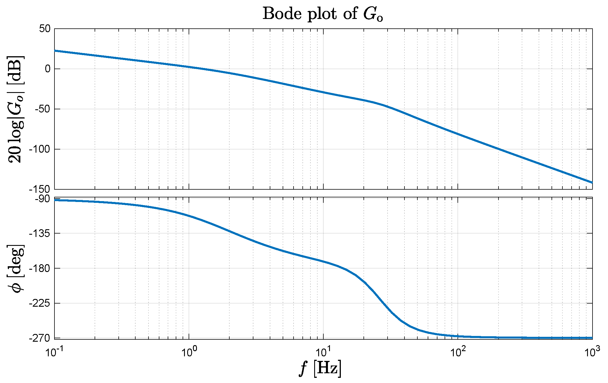
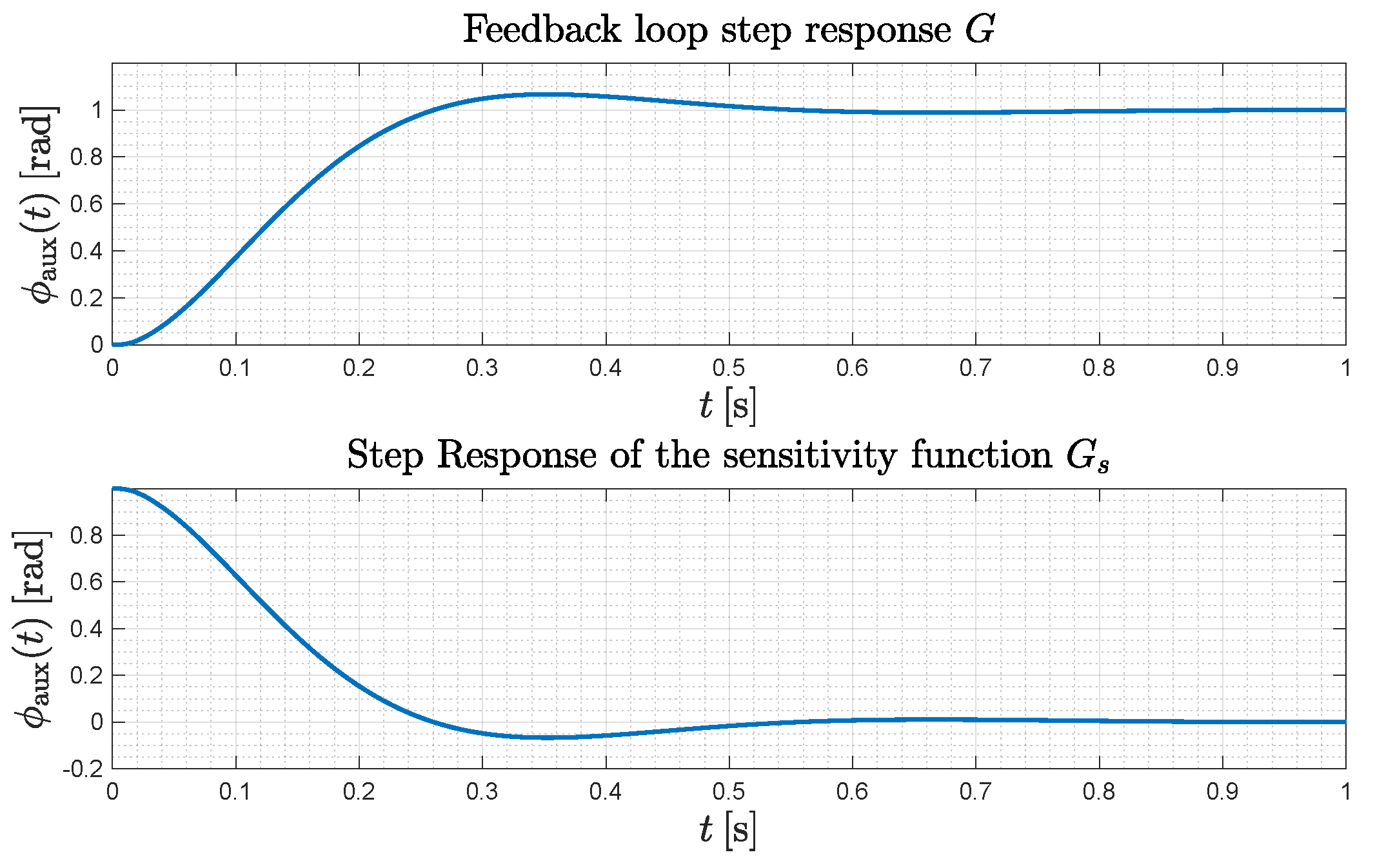
The closed-loop performance of the system can be seen from the Bode plot of the open-loop gain G o , shown in Figure 16, and from the step response G of feedback systems, shown in Figure 17. The rejection of the feedback system to disturbances can be seen in the step response of the sensitivity transfer function G s .
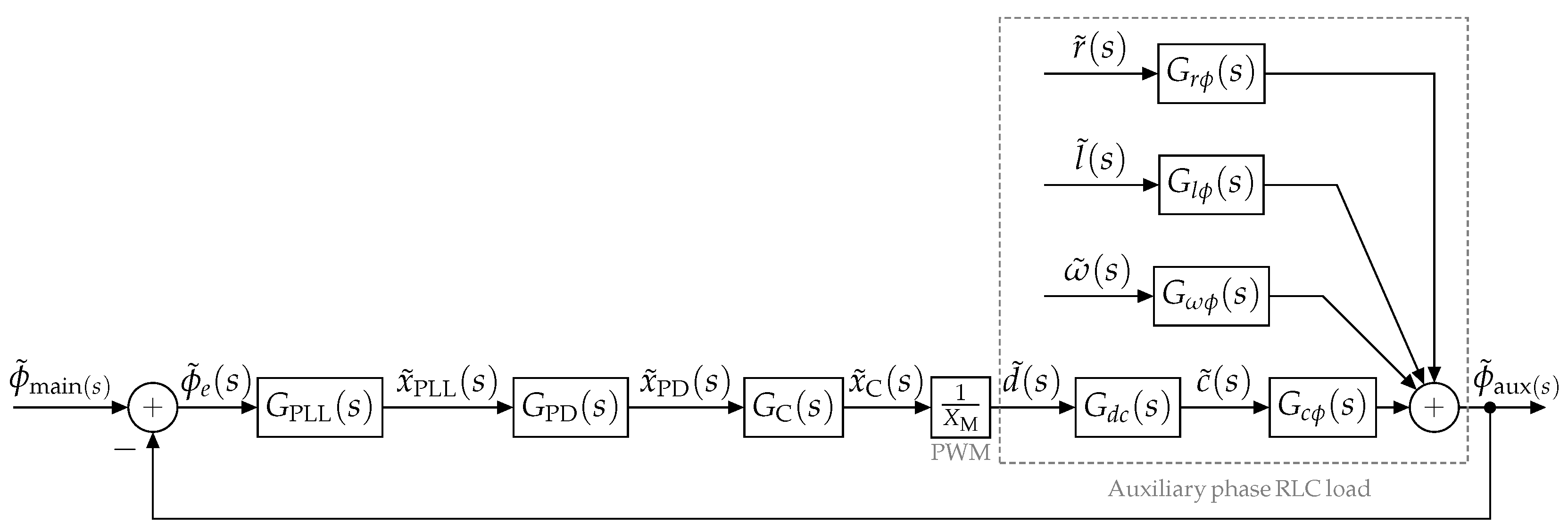
A linearized block diagram of the feedback system is shown in Figure 18 and parameters of the system are shown in Table 1. The calculated gain functions for the operating point are shown in Table 2.
The robustness of the designed PI controller and the whole feedback loop to changes of the system parameters can be seen on the Gain margins G m and phase margins P m , in Table 3 and Table 4.

4. Simulation of the System with an Active IM Load

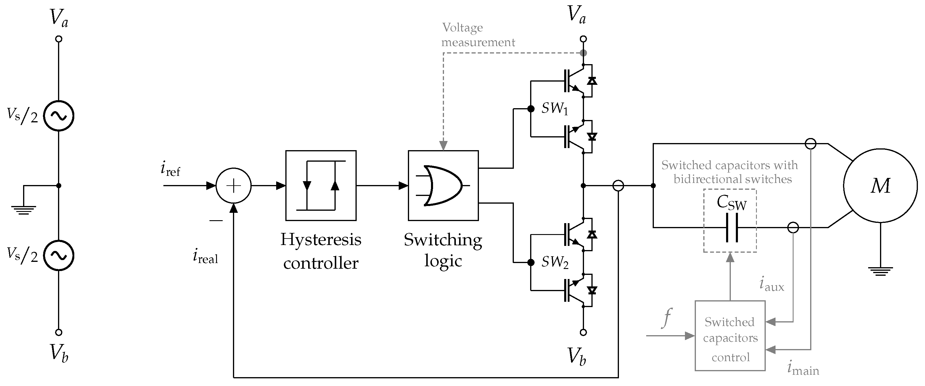
Simulation of single-leg two-phase matrix converter has been done with an active two-phase induction motor load using MATLAB/Simulink environment. The principal scheme is shown in Figure 19 [1,2,3,17,18,19,20]. We have two feedback loops. The first feedback loop controls the common current of both phases with a hysteresis controller. The second control loop controls the phase shift of the currents in both phases. The control methods are described in previous sections. The simulation results are shown in Figure 20, Figure 21 and Figure 22. The calculation time step of the simulation is T s = 1 × 10 5 s .
The parameters for the two-phase induction motor used in simulation and experimental verification are shown in Table 5.

5. Experimental Verification and Measurement

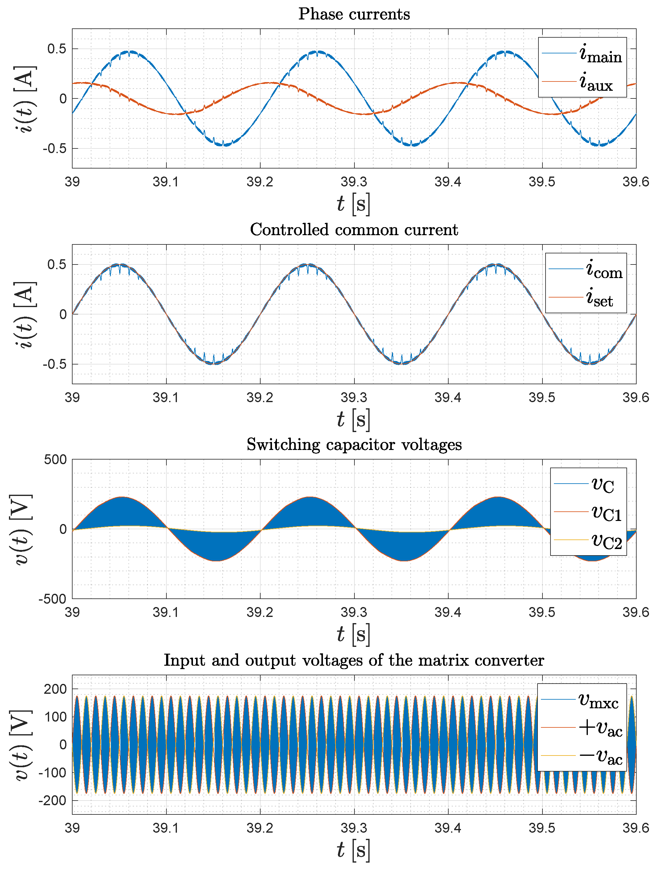
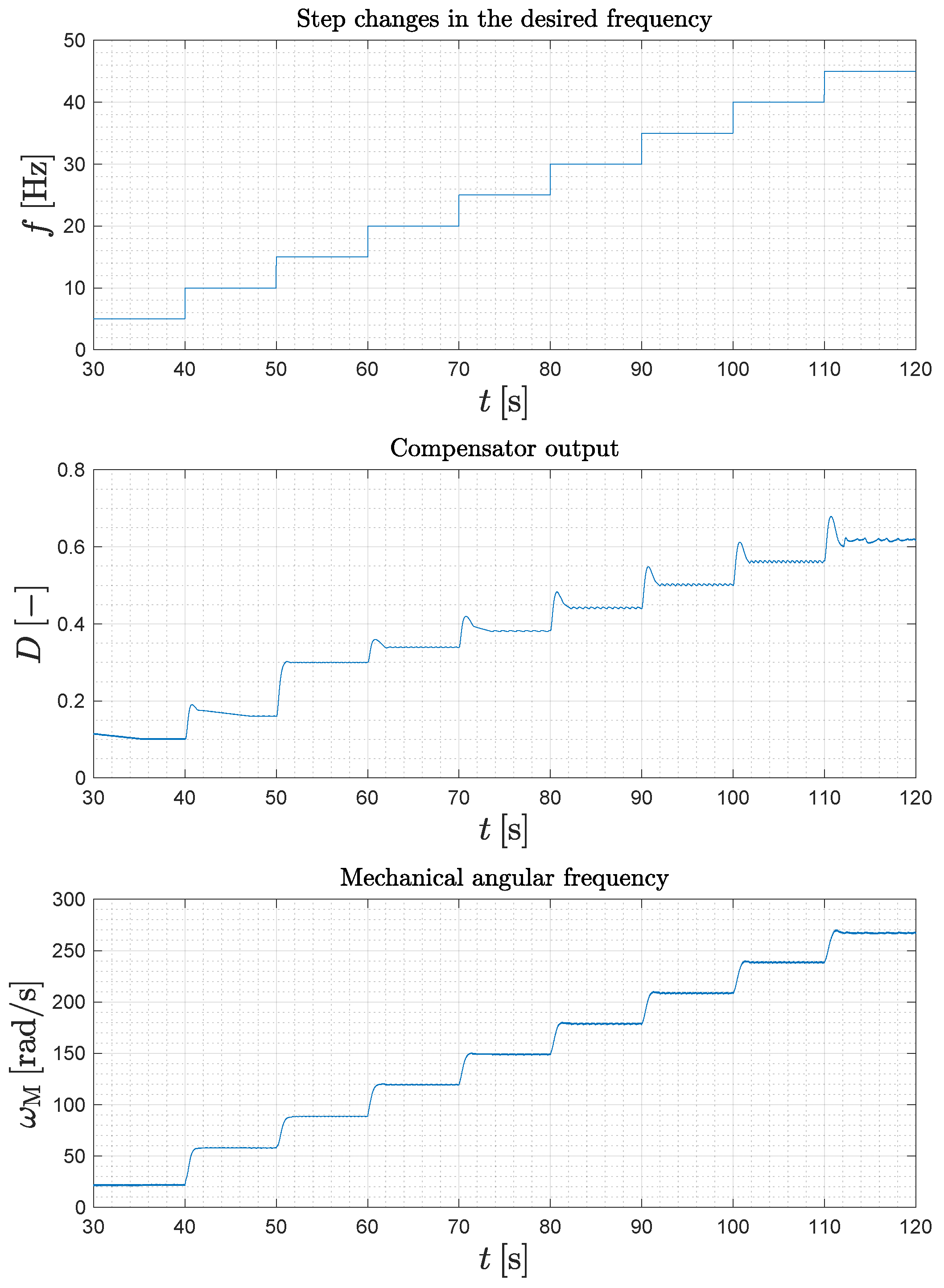
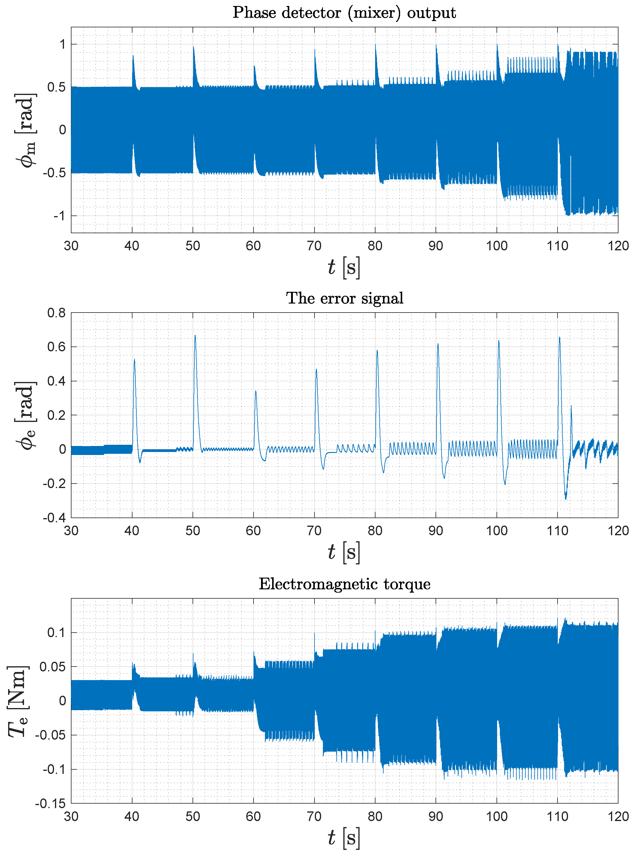
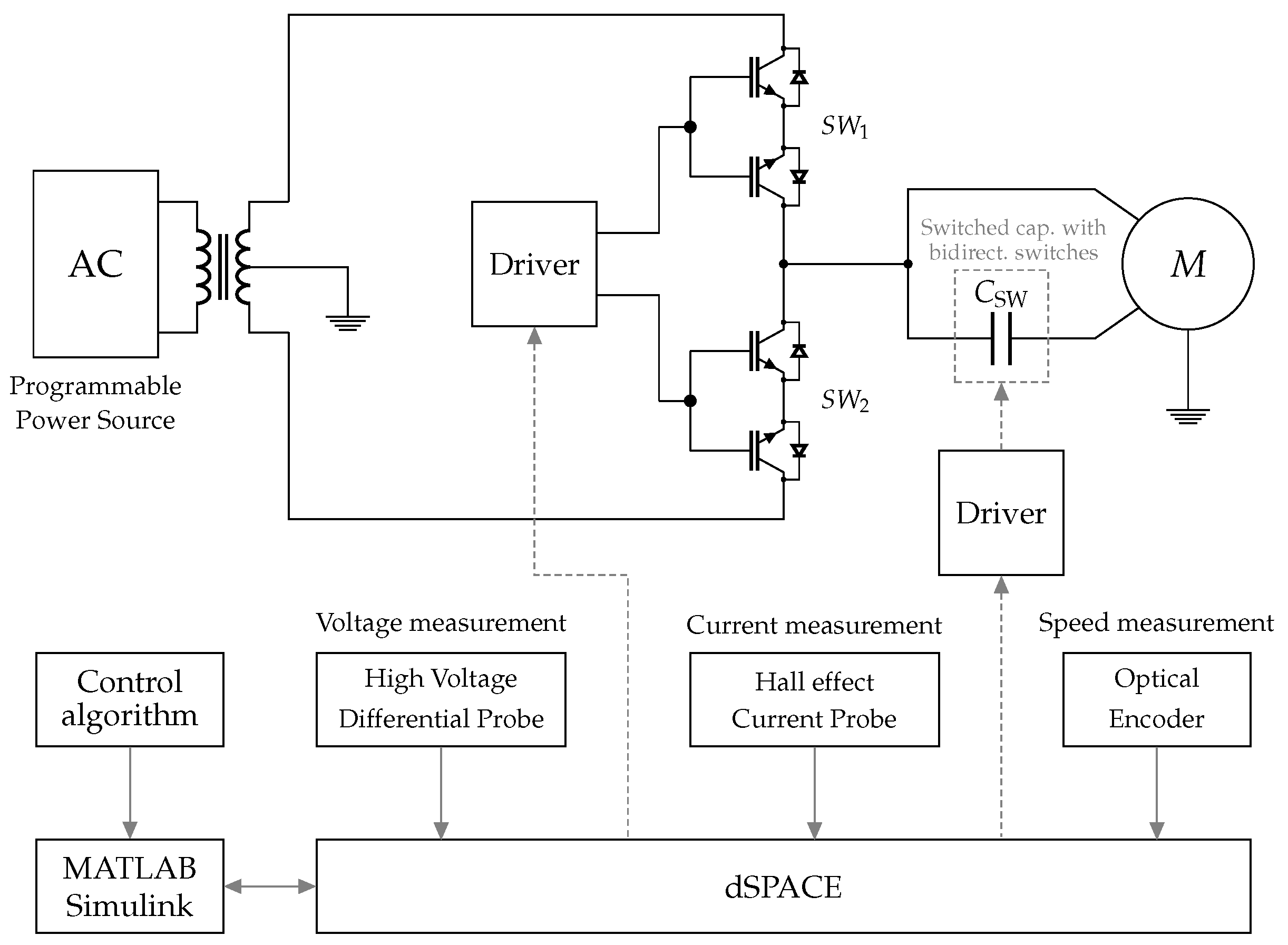
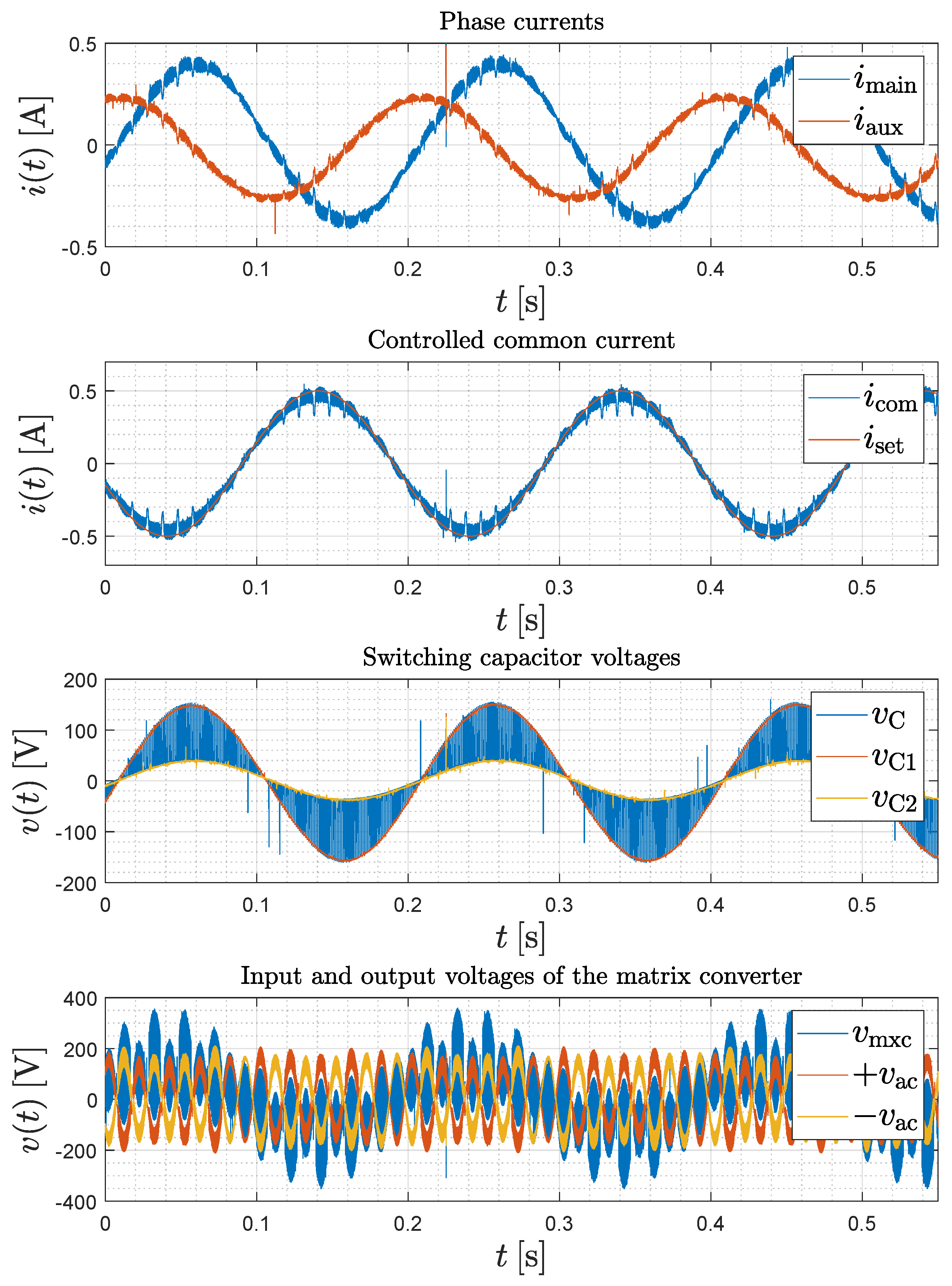
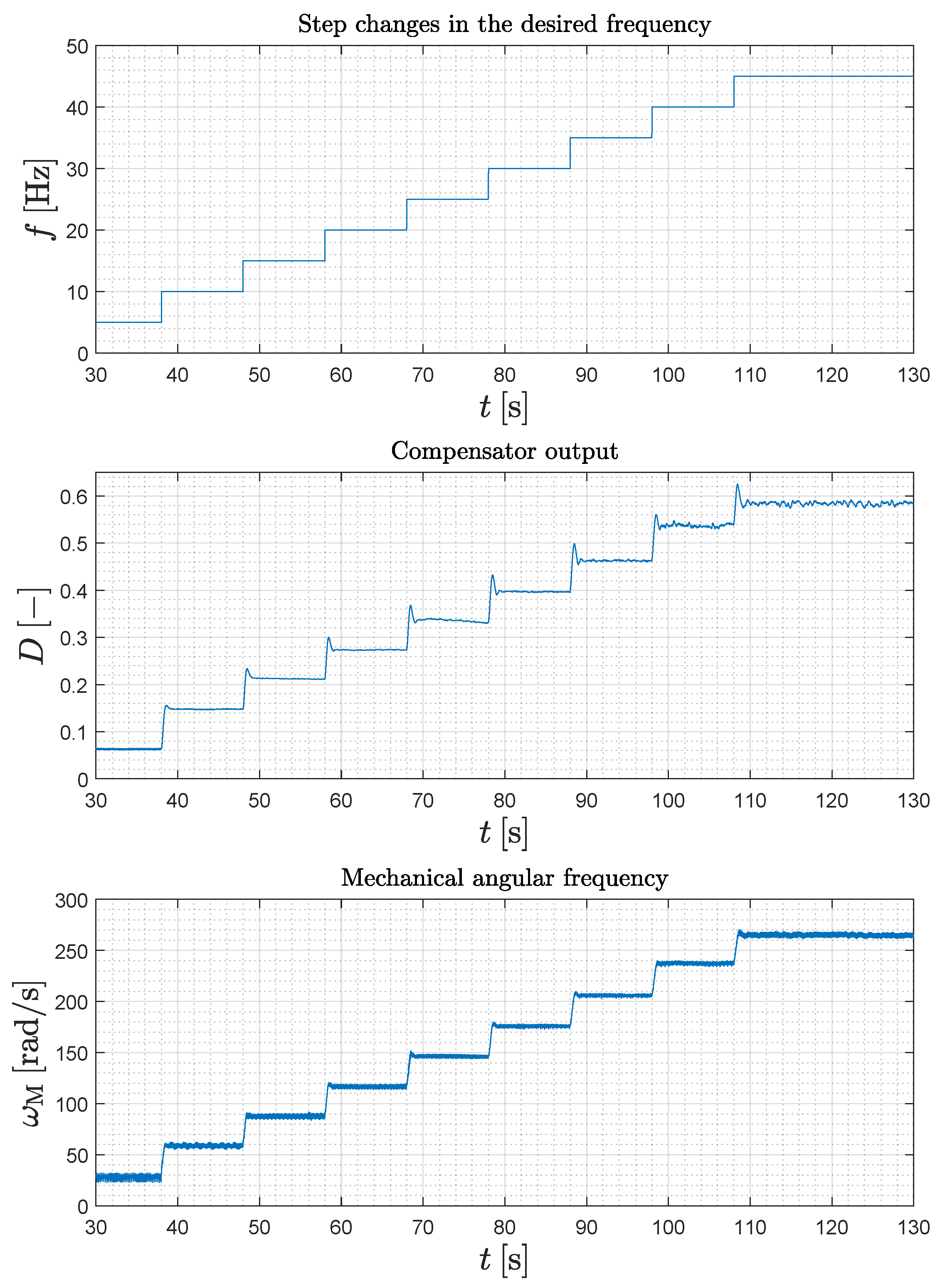
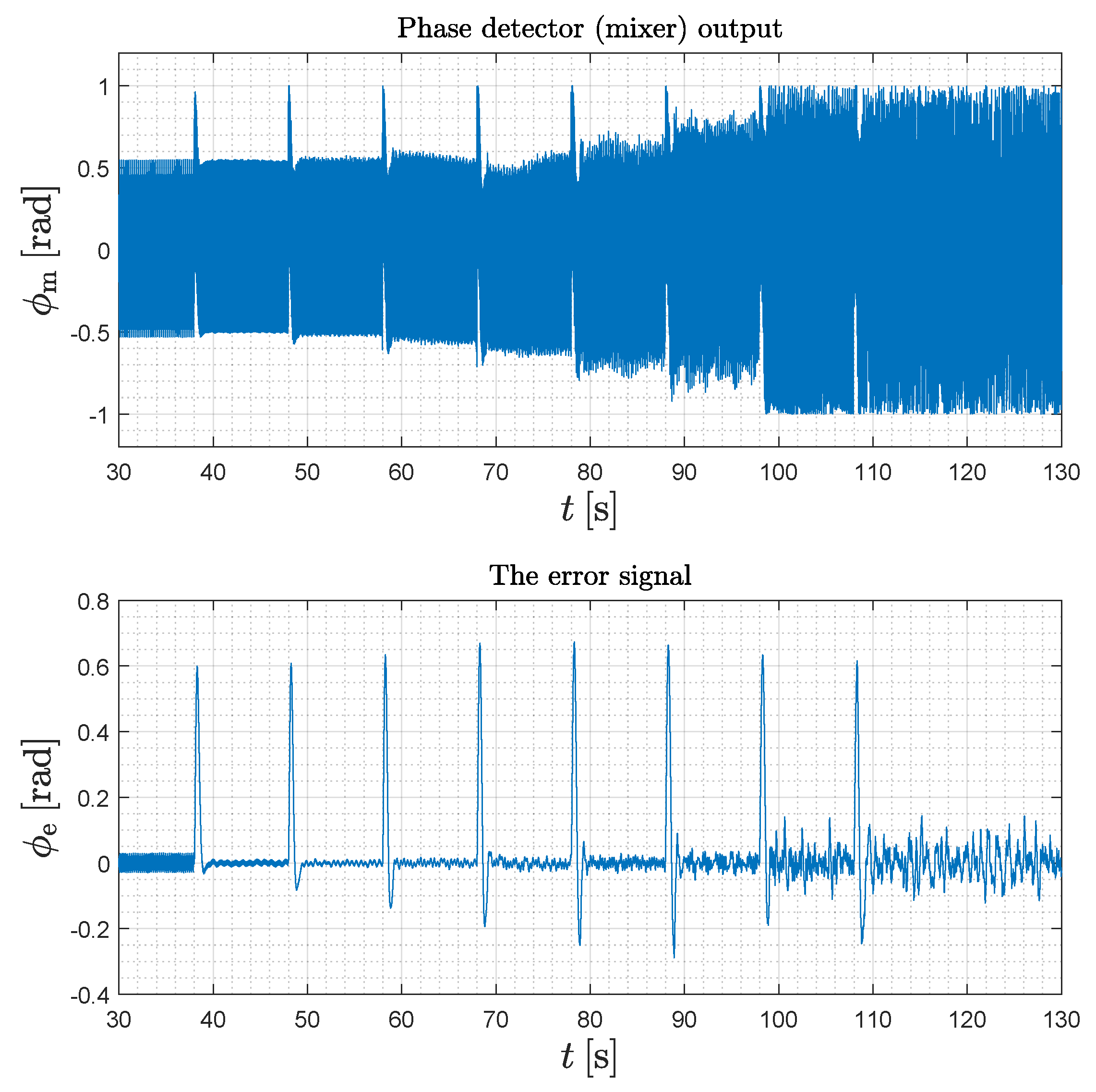
Experimental verification was done with the help of dSPACE hardware interface. The connection with a physical matrix converter and induction motor can be seen in the block scheme in Figure 23. Hall effect current probes with amplifier where used for current measurement and differential voltage probes for voltage measurement. The current and voltage probes were connected to the analog input of dSPACE hardware. The digital outputs of dSPACE were used as the control outputs for the switched capacitors current phase control and hysteresis current control and connected to the transistor drivers. Emitter connected IGBT transistors were used as bidirectional switches for the single-leg matrix converter output and for the switched capacitors. The complete real-time control and measurement were done thru the dSPACE hardware and MATLAB/Simulink, ControlDesk software. The control algorithms were set up in the MATLAB/Simulink environment, and after compilation used in dSPACE. The measured data were saved and then plotted in MATLAB. The calculation time step of dSPACE was T s = 2 × 10 5 s . The calculation time step affects the hysteresis band, that is the reason that the current ripple is higher in real measurement than in the simulation. The experimental results are shown in Figure 24, Figure 25 and Figure 26.

6. Conclusions

This paper brings analysis, modeling, computer simulation, and experimental verification of an enhanced one-leg two-phase matrix converter by a switched capacitor supplied by a symmetrical two-phase network with a neutral point. One of the main contributions is the combined control of the auxiliary phase advancing with 90 degrees phase shift under the entire range of the load operation. Against works with single-leg VSI converters (e.g., [1,2,3]), this paper also completes the topology by switched capacitors controlled to obtain quadrature current for the two-phase output.
Two new methods for controlling the phase shift with the auxiliary phase capacitor have been developed. The first method uses the open-loop control where the phase shift is controlled with a calculated value of capacitance for known parameters of the load (resistance and inductance) and the frequency. The value of capacitance is then set in the switched capacitor. The second method uses a negative feedback loop, where the phase shift automatically tunes to 90 degrees. Improved design of the switching capacitor has also been done with the use of the averaging method to get precise values of the switched capacitance.
Regarding electromagnetic interfacing and compatibility, the solving of those is a demanding problematic [21,22], and was not the subject of this article. Supposed applications of this investigated type of MxC converter are in the field of supply of two-phase induction motors for, e.g., pumps, compressors, etc. in a resident environment. A measurement of electromagnetic interference (EMI)/electromagnetic compatibility (EMC) is important for the prototype version of the converter. We are preparing the infrastructure for such a measurement on real prototype completed by EMI filter at the EMI/EMC chamber in the near future.
The simulations have been done in the MATLAB/Simulink environment. Due to simplification, a passive RL load and harmonic voltage source were first used for the analysis, modeling, and simulation with the switched capacitor. However, we realize that in a real situation is the switched capacitor used with a matrix converter and an active motoric load. Therefore, the final simulation and experimental verification with dSPACE are done with the matrix converter and induction motor as the active load.
The derived control methods with the switched capacitor can also be used with a different type of power converter such as the single-leg two-phase voltage source inverter.
References

Author Contributions

Validation, M.P.; formal analysis, R.K. and J.S.; writing—original draft preparation, R.K.; visualization, R.K.; and supervision, B.D.

Funding

This work was supported by project ITMS: 26210120021, co-funded from EU sources and European Regional Development Fund and projects APVV 0396-15 (Research of perspective high-frequency converter systems with GaN technology) and KEGA 027ŽU-4/2018 (Modelling, Design and Implementation of the Modern Method in the Educational Process of the Technical Faculties Focusing on Discrete Control of Power Systems).

Conflicts of Interest

The authors declare no conflict of interest.

References

  1. Chomat, M.; Lipo, T. Adjustable-speed single-phase IM drive with reduced number of switches. In Proceedings of the 2001 IEEE Industry Applications Conference, Chicago, IL, USA, 30 September–4 October 2001; pp. 1800–1806. [Google Scholar] [CrossRef]
  2. Chomat, M.; Lipo, T. Adjustable-speed drive with single-phase induction machine for HVAC applications. In Proceedings of the 2001 IEEE 32nd Annual Power Electronics Specialists Conference, Vancouver, BC, Canada, 17–21 June 2001; pp. 1446–1451. [Google Scholar] [CrossRef]
  3. Chomat, M.; Lipo, T. Adjustable-speed single-phase IM drive with reduced number of switches. IEEE Trans. Ind. Appl. 2003, 39, 819–825. [Google Scholar] [CrossRef]
  4. Dobrucky, B.; Laskody, T.; Prazenica, M. A novel supply system for two-phase induction motor by single leg matrix converter. Elektron. Elektrotech. 2015, 21, 13–16. [Google Scholar] [CrossRef]
  5. Stefanec, P.; Dobrucky, B. One leg MxC analysis and modelling. In Proceedings of the 2015 International Conference on Electrical Drives and Power Electronics (EDPE), Tatranska Lomnica, Slovakia, 21–23 September 2015. [Google Scholar] [CrossRef]
  6. Kascak, S.; Dobrucky, B.; Prazenica, M.; Radvan, R.; Spanik, P. Bidirectional Switch with the Use of Reverse Function Mode in MOSFET Transistors; Utility Model No. 6899; Industrial Property Office of the Slovak Republic: Banská Bystrica, Slovakia, 2014; (In Slovak Language). [Google Scholar]
  7. Vodovozov, V.; Lillo, N.; Raud, Z. Single-phase electric drive for automotive applications. In Proceedings of the 2014 International Symposium on Power Electronics, Electrical Drives, Automation and Motion SPEEDAM, Ischia, Italy, 18–20 June 2014. [Google Scholar] [CrossRef]
  8. Konarik, R. Single-Leg Matrix Converter: Analysis, Modeling, and Feedback Control. Ph.D. Thesis, Department of Mechatronics and Electronics, Faculty of Electrical Engineering, University of Zilina, Žilina, Slovakia, 2018. [Google Scholar]
  9. Konarik, R.; Dobrucky, B.; Prazenica, M.; Kascak, S. Improved design of switched capacitors for power electronics converters. In Proceedings of the 2018 ELEKTRO, Mikulov, Czech Republic, 21–23 May 2018; pp. 1–6. [Google Scholar]
  10. Lettenmaier, T.; Novotny, D.; Lipo, T. Single phase induction motor with an electronically controlled capacitor. In Proceedings of the Conference Record of the 1988 IEEE Industry Applications Society Annual Meeting, Pittsburgh, PA, USA, 2–7 October 1988. [Google Scholar] [CrossRef]
  11. Suciu, C.; Kansara, M.; Holmes, P.; Szabo, W. Performance enhancement of an induction motor by secondary impedance control. IEEE Trans. Energy Convers. 2002, 17, 211–216. [Google Scholar] [CrossRef]
  12. Danila, A.; Margineanu, I.; Campeanu, R.; Suciu, C.; Boian, I. The optimization of the single/two phase induction motor start-up with electronically switched capacitor. In Proceedings of the 2008 IEEE International Conference on Automation, Quality and Testing, Robotics, Cluj-Napoca, Romania, 22–25 May 2008. [Google Scholar] [CrossRef]
  13. Suciu, C.; Kansara, M.; Holmes, P.; Szabo, W. Phase advancing for current in R-L circuits using switched capacitors. Electron. Lett. 1999, 35, 1296. [Google Scholar] [CrossRef]
  14. Franklin, G.F.; Powell, J.D.; Emami-Naeini, A. Feedback Control of Dynamic Systems, 7th ed.; Pearson: London, UK, 2014. [Google Scholar]
  15. Gray, P.; Hurst, P.; Lewis, S.; Meyer, R. Analysis and Design of Analog Integrated Circuits, 5th ed.; Wiley: Hoboken, NJ, USA, 2009. [Google Scholar]
  16. Erickson, R.W.; Maksimovic, D. Fundamentals of Power Electronics, 2nd ed.; Springer: Berlin, Germany, 2001. [Google Scholar]
  17. Zuckerberger, A.; Weinstock, D.; Alexandrovitz, A. Single-phase matrix converter. IEE Proc. Electr. Power Appl. 1997, 144, 235–240. [Google Scholar] [CrossRef]
  18. Reveles-Miranda, M.; Flota-Bañuelos, M.; Chan-Puc, F.; Pacheco-Catalán, D. Experimental Evaluation of a Switching Matrix Applied in a Bank of Supercapacitors. Energies 2017, 10, 2077. [Google Scholar] [CrossRef]
  19. Peretti, G.; Romero, E.; Marqués, C. On the ability of oscillation-based test for detecting deviation faults in switched-capacitor ladder filters. Electr. Eng. 2007, 90, 127–141. [Google Scholar] [CrossRef]
  20. Rajki, I.; Vas, P. Increasing the starting torque of capacitor-run split-phase induction machines by a positive temperature coefficient (PTC) resistor. Arch. Elektrotech. 1984, 67, 65–69. [Google Scholar] [CrossRef]
  21. Tarateeraseth, V.; See, K.Y.; Canavero, F.G.; Chang, R.W.Y. Systematic Electromagnetic Interference Filter Design Based on Information From In-Circuit Impedance Measurements. IEEE Trans. Electromagn. Compat. 2010, 52, 588–598. [Google Scholar] [CrossRef] [Green Version]
  22. Saponara, S.; Ciarpi, G.; Groza, V.Z. Design and experimental measurement of EMI reduction techniques for integrated switching DC/DC converters. Can. J. Electr. Comput. Eng. 2017, 40, 116–127. [Google Scholar]
Figure 1. A switched capacitor with: (a) two switches; and (b) one ideal single-pole double-throw switch.
Energies 11 02761 g001
Figure 2. A symbolic equivalent of a four-quadrant switch with emitter connected IGBT transistors.
Energies 11 02761 g002
Figure 3. A capacitor connected to a voltage source: (a) single capacitor; and (b) switched capacitor equivalent.
Energies 11 02761 g003
Figure 4. A capacitor connected to a current source: (a) single capacitor; and (b) switched capacitor equivalent.
Energies 11 02761 g004
Figure 5. A harmonic voltage source with a capacitor and RL load in series: (a) single capacitor; and (b) switched capacitor equivalent.
Energies 11 02761 g005
Figure 6. A harmonic voltage source with two-phase RL load and switched capacitors.
Energies 11 02761 g006
Figure 7. The method of conservation of energy for current phase advancing.
Energies 11 02761 g007
Figure 8. The averaging method for current phase advancing.
Energies 11 02761 g008
Figure 9. The variable capacitance of the switched capacitors as a function of the duty cycle for both methods.
Energies 11 02761 g009
Figure 10. Vector diagram of calculation for a fixed 90 degrees phase shift of current.
Energies 11 02761 g010
Figure 11. Vector diagram of calculation for a variable phase shift of current.
Energies 11 02761 g011
Figure 12. Block diagram of the open-loop control of current phase advancing.
Energies 11 02761 g012
Figure 13. A simplified block diagram of the open-loop control of current phase advancing.
Energies 11 02761 g013
Figure 14. Block diagram of the closed-loop control of current phase advancing with the mixer as a phase detector.
Energies 11 02761 g014
Figure 15. A simplified block diagram with nonlinearities of the closed-loop control of current phase advancing with the mixer as a phase detector.
Energies 11 02761 g015
Figure 16. Bode plot of open-loop gain function.
Energies 11 02761 g016
Figure 17. Step response of control transfer function and sensitivity function.
Energies 11 02761 g017
Figure 18. A linearized block diagram of the closed-loop (feedback) control of current phase advancing.
Energies 11 02761 g018
Figure 19. Matrix converter with an active induction motor load.
Energies 11 02761 g019
Figure 20. Simulated variables of phase shift feedback control at a frequency of 5 Hz.
Energies 11 02761 g020
Figure 21. Simulated step-up response of the phase shift feedback control.
Energies 11 02761 g021
Figure 22. Simulated step-up error response of the phase shift feedback control.
Energies 11 02761 g022
Figure 23. Experimental verification and measurement of the matrix converter with dSPACE hardware.
Energies 11 02761 g023
Figure 24. Measured variables of feedback control at a frequency of 5 Hz.
Energies 11 02761 g024
Figure 25. Measured step-up response of the feedback control.
Energies 11 02761 g025
Figure 26. Measured step-up error response of the feedback control.
Energies 11 02761 g026
Table 1. Parameters of the controlled system.
ParametersValuesUnits
f25 Hz
R 1 59.58 Ω
R 2 67.38 Ω
L 1 1210 mH
L 2 2045 mH
C 1 2.5 μ F
C 2 200 μ F
Table 2. Gain functions of the linearized control system.
ParametersValuesUnits
G d c 9.7265 × 10 5 F
G c ϕ 2.4878 × 10 5 rad / F
G d ϕ 24.1979 rad
G ω ϕ −0.0571 s
G l ϕ −2.1227 rad / H
G r ϕ 0.0580 rad / Ω
Table 3. Gain margin at different parameters of the system.
Gm (dB) L 2 (mH)
10 % 2045 + 10 %
f (Hz)554.15149.3
2534.634.233.7
453433.533.1
Table 4. Phase margin at different parameters of the system.
Pm (deg) L 2 (mH)
10 % 2045 + 10 %
f (Hz)587.28685.1
2563.161.960.8
4561.460.259.1
Table 5. Parameters of the induction motor.
ParametersValuesUnits
P n 150 VA
V rms 230 V
f50 Hz
R s 59.58 Ω
R S 67.38 Ω
L ss 1210 mH
L SS 2045 mH
L ms 1120 mH
L mS 1471 mH
J 488 × 10 6 kg · m 2
F 10 × 10 6 N · m · s
p p 1
N s / N S 1.6