Article

Bidirectional Resonant Converter with Half-Bridge Circuits: Analysis, Design, and Implementation

Department of Electrical Engineering, National Yunlin University of Science and Technology, Yunlin 640, Taiwan
*
Author to whom correspondence should be addressed.
Energies 2018, 11(5), 1259; https://doi.org/10.3390/en11051259
Submission received: 24 April 2018 / Revised: 10 May 2018 / Accepted: 14 May 2018 / Published: 15 May 2018

Abstract

:
A soft-switching dc–dc converter with bidirectional power flow capability is studied in this paper for energy storage units or electric vehicle applications. The circuit topology of the studied converter is constructed using a dual half-bridge circuit with split capacitors. A series resonant tank with frequency control modulation is employed in the proposed circuit to realize the soft switching characteristics of active devices. Synchronous-rectifier-based Metal-Oxide-Semiconductor Field-Effect Transistor (MOSFETs) are used on the low-voltage side to lessen conduction loss on the power semiconductors. The benefits of the studied circuit are bidirectional power flow capability, high efficiency, low switching loss, and simple circuit structure. The achievability of the developed converter is demonstrated from test results with a scaled-down laboratory prototype.

1. Introduction

Clean energy sources have been developed to lessen the demand of fossil fuel, reduce environmental air pollution, and decrease climate change. Therefore, power-electronics-based energy conversion has been researched and studied to increase energy conversion efficiency and reduce circuit size. For ac or dc microgrid systems [1,2,3,4,5], dc/dc converters, ac/dc converters, and dc/ac converters are needed to integrate the utility power, wind power, solar power, energy storage units, and residential loads. For electric vehicles [6,7,8,9], ac/dc converters are employed for the battery charger, dc/dc converters are adopted on the dc power distributing system, and dc/ac converters are used for ac motor drives. Bidirectional dc/dc converters [10,11,12,13,14,15] are widely used for battery-based energy storage units in dc microgrid systems and electric vehicles. Normally, bidirectional dc/dc converters are adopted to transfer electric energy between high voltage dc buses and energy storage units. Among the circuit topologies of bidirectional dc/dc converters, the half-bridge topologies and full-bridge topologies are most attractive solutions to realize bidirectional power flow capability. Phase-shift pulse-width modulation (PWM) is usually selected in full-bridge converters. However, high circulating current losses and high switching losses on light load are the main shortcomings. Resonant converters [16,17,18,19] with frequency modulation have been studied to achieve soft switching characteristics and bidirectional power flow capability. However, the circuit characteristics under forward and reverse power flow directions are different. Thus, the design procedures of bidirectional resonant converters are more difficult. In [16], the characteristic of a series resonant converter was achieved in forward power flow (or buck operation). However, the characteristic of a series resonant converter cannot be achieved at the whole load range in reverse power flow (or boost operation) due to the circuit topologies in the buck and boost operations not being symmetric circuits. In [17,18,19], the circuit topologies with half-bridge or full-bridge converters in both power flows are symmetric so that the power devices can be turned on under zero voltage and low switching losses. However, one more inductor is connected to the switching leg so that high circulating current is introduced and conduction losses are increased. Therefore, the circuit efficiency is reduced.
A bidirectional dc/dc converter with a frequency modulation scheme is studied to realize the features of bidirectional power flow capability and zero-voltage switching. A dual half-bridge circuit is used in the studied circuit to realize bidirectional power flow. A series resonant tank is adopted on the high-voltage side to realize the soft switching characteristics for all active devices. Synchronous rectifiers are used on the low-voltage side to further reduce the conduction loss. In order to realize the same resonant characteristics under forward and reverse power flow directions, an ac power switch and parallel inductor are connected to the half-bridge leg on the high-voltage side. The proposed circuit and the conventional bidirectional resonant converters in [17,18,19] have the same resonant component counts. However, the proposed converter has less circulating current loss due to the fact that the parallel inductor is disconnected under forward power flow. The circuit topology of the studied circuit is simple and easy to implement. In Section 2, the circuit configuration, operating stages, and circuit characteristics of the proposed converter are discussed. In Section 3, the design procedures of the developed converter are provided. Experimental waveforms are demonstrated in Section 4, and conclusions are discussed in Section 5.

2. Proposed Converter

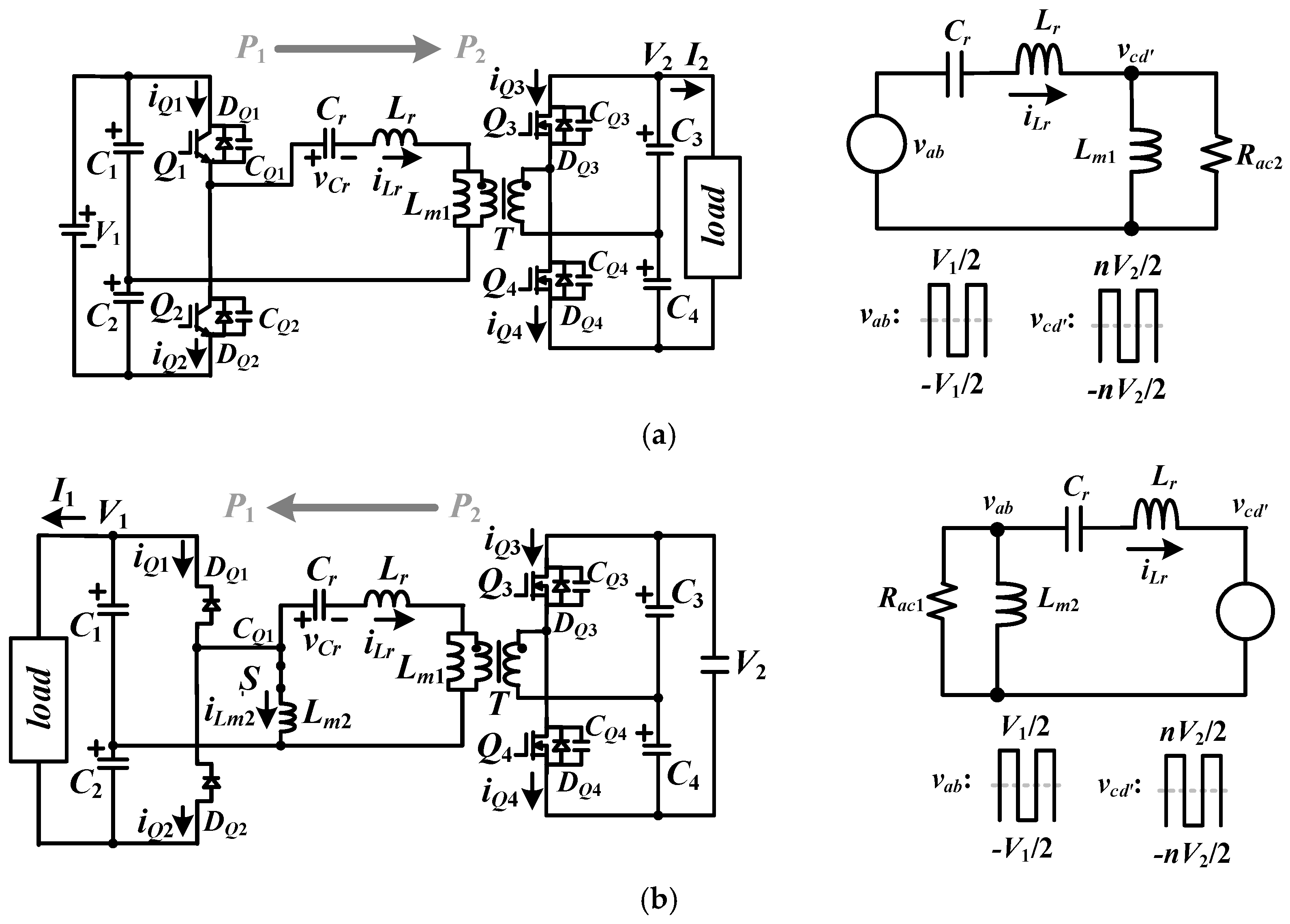
The circuit schematic of the studied dual half-bridge converter is provided in Figure 1 to realize bidirectional power flow. Two half-bridge circuits are used on both the high- and low-voltage sides and one resonant tank is adopted on the high-voltage side to achieve the soft switching characteristic under frequency control. If power is transferred from high-voltage V1 to low-voltage V2 as shown in Figure 2a, the ac switch S is open and the dual half-bridge converter is worked under buck mode operation. Q1 and Q2 are main power devices and Q3 and Q4 are operated as synchronous rectifiers. Lr, Cr, and Lm1 are operated as an LLC resonant converter to have low switching losses and high circuit efficiency functions. If power is transferred from low-voltage V2 to high-voltage V1 as shown in Figure 2b, the ac switch S is closed and the dual half-bridge converter is worked under boost mode operation. Under this condition, Q3 and Q4 are the main power devices, Q1 and Q2 are off, and the antiparallel diodes are worked as the full-wave rectifier. Lr, Cr, and Lm2 are operated as an LLC resonant converter to give low switching losses and high circuit efficiency functions.

2.1. Forward Power Flow

The studied dual half-bridge converter can achieve bidirectional power flow capability. When power is transferred from high-voltage V1 to low-voltage V2, battery banks or super capacitors can be adopted as energy storage units on the low-voltage terminal. The circuit configuration of the adopted dual half-bridge converter under forward power flow is shown in Figure 2a. The ac switch S is off under forward power flow. Q1 and Q2 are worked as the main switches to generate a square wave voltage on voltage vab. Q3 and Q4 are operated as synchronous rectifiers to lessen conducting losses on the low-voltage side. According to the polarity of the secondary side current, a square wave voltage is generated on voltage vcd’. Lm1 is the magnetizing inductance of the transformer; Lr and Cr are the resonant inductor and capacitor. Q1 and Q2 are controlled by using frequency modulation to regulate load current I2 or voltage V2. Due to the resonant operation by Lr, Cr, and Lm1, the soft switching operation of Q1 and Q2 can be realized. Figure 3a demonstrates the basic PWM signals of the studied converter under forward power flow operation. If the series resonant frequency is higher (or lower) than the operating frequency, there are six (or four) operation stages per switching cycle as shown in Figure 3b–g. The circuit operations of the studied circuit under forward power flow are presented in the following.
Stage 1 (t0~t1): The output voltage of CQ1 is decreased to zero at t0. Therefore, the soft switching characteristic of Q1 can be achieved after t0 due to iQ1 (t0) = iLr (t0) < 0 and DQ1 conducts. Since iLr > iLm1 and iQ3 < 0, Q3 is turned on and the secondary side current flows through MOSFET Q3 turn-on resistor Ron to charge capacitor C3. Due to low turn-on resistance Ron, the conduction losses on the low-voltage side can be reduced compared to using a fast recovery diode. The ac side voltages of the two half-bridge circuits are vab = VC1 = V1/2 and vcd = VC3 = V2/2. Thus, the primary magnetizing voltage vLm1 = vcd = nV2/2 and the magnetizing current iLm1 increase with the current slope nV2/(2Lm1). The magnetizing current variation in Stage 1 is about ΔiLm1,1 = nV2Δt10/(2Lm1) where Δt10 is the time interval in Stage 1. Cr and Lr are resonant in Stage 1 under vab = V1/2, vLm1 = nV2/2 and f r = 1 / 2 π C r L r . If fr > fsw, then Tr/2 < Tsw/2. Therefore, the transformer secondary current will decrease to zero before Q1 turns off. The circuit operation goes to Stage 2. If fr < fsw, then Tr/2 > Tsw/2. When Q1 turns off, the secondary winding current is still positive. Then, the circuit operation goes to Stage 3.
Stage 2 (t1~t2): If fr > fsw, the transformer secondary current decreases to zero before Q1 turns off. When iQ3 equals zero at t1, Q3 turns off. iLr flows through Q1, Cr, Lr, Lm1, and C1. Since C1 >> Cr, components Cr, Lr, and Lm1 are resonant under vab = V1/2 and resonant frequency f p = 1 / 2 π C r ( L r + L m 1 ) . When t = Tsw/2, switch Q1 turns off and the circuit operation of Stage 2 is completed.
Stage 3 (t2~t3): When t = t2 = Tsw/2, Q1 turns off, and CQ1 (CQ2) is charged (discharged) by iLr. In order to ensure that Q2 turns on at zero voltage, the zero-voltage condition of Q2 is calculated using
i L m 1 , p e a k V 1 2 2 C Q L m 1 + L r
where CQ = CQ1 = CQ2. The maximum magnetizing current is estimated using Equation (2).
i L m 1 , p e a k = Δ i L m 2 n V 2 8 L m 1 f s w
The time interval in Stage 3 can be estimated as follows when CQ2 is discharged to zero voltage:
Δ t 23 = 2 V 1 C Q i L r ( t 2 ) 2 V 1 C Q i L m 1 , p e a k = 16 L m 1 f s w V 1 C Q n V 2 t d e a d
where tdead is the dead time between Q1 and Q2. Based on Equation (3), the maximum magnetizing inductance Lm1 can be calculated using Equation (4).
L m 1 t d e a d n V 2 16 f s w V 1 C Q
Stage 4 (t3~t4): The voltage of CQ2 is decreased to zero at t3. The body diode DQ2 conducts due to iLr (t3) > 0 (or iQ2 (t3) < 0). After time t3, the soft switching characteristic of Q2 can achieved. Since the secondary side current iQ4 is negative, Q4 is forced to turn on to decrease conduction loss. Then, the ac side voltage vcd = −V2/2, the magnetizing voltage vLm1 = −nV2/2, and iLm1 decreases. The magnetizing current variation in Stage 2 is about ΔiLm1,4 = nV2Δt34/(2Lm1) where Δt34 is the time interval in Stage 4. In Stage 4, Cr and Lr are resonant under vab = −V1/2, vLm1 = −nV2/2 and f r = 1 / 2 π C r L r . If fr > fsw, the circuit operation goes to Stage 5. If fr < fsw, the circuit operation goes to Stage 6.
Stage 5 (t4~t5): If fr > fsw, iQ4 will go to zero before Q2 turns off. When iQ4 equals zero at t4, Q4 is forced to turn off. In Stage 5, iLr flows through Q2, Cr, Lr, Lm1, and C2. Components Cr, Lr, and Lm1 are resonant under vab = −V1/2 with resonant frequency f p = 1 / 2 π C r ( L r + L m 1 ) . When Q2 turns off, the circuit operation goes to Stage 6.
Stage 6 (t5~Tsw + t0): When Q2 turns off at t5, CQ1 (CQ2) is discharged (charged) by iLr (t5) < 0. To ensure that Q1 turns on at zero voltage, the zero-voltage condition of Q1 is the same as that of Q2. The time interval in this stage is short enough to be neglected in state–state analysis. At time Tsw + t0, the voltage of CQ1 decreases to zero voltage and the circuit operation of this stage is completed.
To derive the transfer function of the studied converter under forward power flow, a fundamental frequency approach is adopted to derive the ac voltage gain. According to the on/off states of Q1~Q4, the square voltage waveforms are obtained on voltages vab and vcd. Since the resonant tank of Lr, Cr, and Lm1 is worked as a band pass filter, the harmonic frequency on vab and vcd can be neglected to simplify the characteristic analysis. The root mean square (rms) values of vab and vcd at the switching frequency are 2 V 1 / π and 2 V 2 n / π , respectively. The equivalent resistance at the primary side of transformer can be calculated as R a c 2 = 2 n 2 R o / π 2 . The equivalent circuit of the adopted resonant tank is shown in Figure 2a. The effectively fundamental sinusoidal voltage is vab,f with rms voltage value 2 V 1 / π and the resonant tank consists of Lr, Cr, Lm1, and Rac2. The voltage transfer function between low-voltage V2 and high-voltage V1 is derived in Equation (5).
G 1 , 2 ( s ) | = v R a c 2 ( s ) v a b , f ( s ) = s L m 1 R a c 2 s L m 1 + R a c 2 1 s C r + s L r + s L m 1 R a c 2 s L m 1 + R a c 2
The amplitude of the voltage transfer function in Equation (5) can be obtained using Equation (6):
| G 1 , 2 ( f s w ) | = k F 2 [ ( k + 1 ) F 2 1 ] 2 + [ Q k F ( F 2 1 ) ] 2
where f r = 1 / ( 2 π L r C r ) , Q = L r / C r / R a c 2 , k = Lm1/Lr, and F = fsw/fr. Based on the input voltage V1, output voltage V2, inductor ratio k, and load resistance Rac2, the necessary switching frequency can be calculated from Equation (6). The gain curve of the proposed converter under forward power flow is plotted in Figure 3h under inductor ratio k = Lm1/Lr = 7.

2.2. Reverse Power Flow

The power flow of the studied dual half-bridge circuit can also be delivered from low-voltage V2 to high-voltage V1 as shown in Figure 2b. Under this condition, the ac switch S is turned on, Q3 and Q4 are operated as the main power switch to generate a square voltage waveform on voltage vcd, and the primary voltage vLm1nvcd = vcd. Q1 and Q2 are off and the antiparallel diodes DQ1 and DQ2 are operated as the full-wave rectifiers. According to the polarity of iQ1 and iQ2, a square wave voltage is generated on voltage vab. Lr, Cr, and Lm2 are activated as the resonant tank to realize an inductive load operation. Therefore, the soft switching characteristic of main power devices Q3 and Q4 can be achieved. Q3 and Q4 are controlled with frequency modulation to regulate current I1 or voltage V1. Figure 4 demonstrates the PWM waveforms and the equivalent circuit of the studied converter under reverse power flow.
Stage 1 (t0~t1): CQ3 is discharged to zero voltage at t0, iLr > 0, and iQ3 < 0. The soft switching characteristic of Q3 is realized when Q3 is turned on after t0. Since −iLr > iLm2 and iQ1 < 0, DQ1 conducts and C1 is charged by −iQ1. In Stage 1, the ac side voltages are vab = VC1 = V1/2 and vcd = VC3 = V2/2. iLm2 increases with the current slope V1/(2Lm2). Cr and Lr are resonant in Stage 1 under vab = V1/2, vLm1 = nV2/2, and f r = 1 / 2 π C r L r . If fr > fsw, the circuit operation goes to the next stage. If fr < fsw, the circuit operation goes to Stage 3. Power is transferred in this stage from V2 to V1 through Q3, T, Lr, Cr, and DQ1.
Stage 2 (t1~t2): When iDQ1 is decreased to zero at t1, DQ1 is reverse biased. iLr flows through S, Cr, Lr, T, and Lm2. Cr, Lr, and Lm2 are resonant under vLm1 = nV2/2 and resonant frequency f p = 1 / 2 π C r ( L r + L m 2 ) . When t = t2, Q3 turns off and the circuit operation of Stage 2 is completed.
Stage 3 (t2~t3):Q3 turns off at time t2. Since iLr < 0, CQ3 (CQ4) is charged (discharged). In order to ensure that Q4 turns on at zero voltage, the zero-voltage condition of Q4 is calculated in Equation (7):
i L m 2 , p e a k V 2 2 2 C Q , s L m 2 + L r
where CQ,s = CQ3 = CQ4. The peak values of iLm1 and iLm2 can be calculated as
i L m 1 , p e a k = Δ i L m 1 2 V 2 8 L m 1 f s w
i L m 2 , p e a k = Δ i L m 2 2 V 1 8 L m 2 f s w .
The time interval in Stage 3 can be estimated when CQ4 is discharged to zero voltage:
Δ t 23 = 2 V 2 C Q , s n [ i L m 1 ( t 2 ) + i L m 2 ( t 2 ) ] 2 V 2 C Q , s n [ i L m 1 , p e a k + i L m 2 , p e a k ] = 16 L m 1 L m 2 f s w V 2 C Q , s n ( L m 2 V 2 + L m 1 V 1 ) t d e a d
where tdead is the dead time between Q3 and Q4.
Stage 4 (t3~t4):CQ4 is discharged to zero at t3. The body diode DQ4 of Q4 conducts due to the fact that iD4 (t3) < 0. Therefore, the soft switching characteristic of Q4 can achieved after time t3. In Stage 4, iQ2 is negative and DQ2 conducts. Therefore, vab = −V1/2 and vcd = −V2/2. Cr and Lr are resonant with resonant frequency f r = 1 / 2 π C r L r . If fr > fsw, the circuit operation goes to Stage 5. If fr < fsw, the circuit operation goes to Stage 6.
Stage 5 (t4~t5): If fr > fsw, iQ2 will go to zero before Q4 is turned off. When iDQ2 equals zero at t4, DQ2 is reverse biased. In Stage 5, iLr flows through Cr, Lr, T, and Lm2. Components Cr, Lr, and Lm2 are resonant under vcd = −V2/2 with resonant frequency f p = 1 / 2 π C r ( L r + L m 2 ) . When Q4 turns off at t5, the circuit operation goes to Stage 6.
Stage 6 (t5~Tsw + t0): When Q4 turns off at t5, CQ3 (CQ4) is discharged (charged). The time interval in Stage 6 can be neglected in state–state analysis. At time Tsw + t0, the voltage of CQ3 is decreased to zero and the circuit operation of Stage 6 is completed.
The transfer function of the studied circuit under reverse power flow is similar to that under forward power flow operation. Q3 and Q4 are the main active devices and DQ1 and DQ2 are worked as the full-wave diode rectifier. The circuit characteristic of Lr, Cr, and Lm2 (instead of Lm1) is like a band pass filter to filter the harmonic current. Figure 2b gives the equivalent circuit of the adopted resonant tank. The effectively fundamental sinusoidal voltage is vcd’,f with rms voltage value 2 V 2 n / π , and the resonant tank consists of Lr, Cr, Lm2, and Rac1. The equivalent resistance at the high-voltage side is calculated as R a c 1 = 2 R o / π 2 . The voltage transfer function between high-voltage V1 and low-voltage V2 is derived in Equation (11).
G 2 , 1 ( s ) | = v R a c 1 ( s ) v c d , f ( s ) = s L m 2 R a c 1 s L m 2 + R a c 1 1 s C r + s L r + s L m 2 R a c 1 s L m 2 + R a c 1
Likewise, the amplitude of the voltage transfer function in Equation (11) can be calculated using Equation (12):
| G 2 , 1 ( f s w ) | = k F 2 [ ( k + 1 ) F 2 1 ] 2 + [ Q k F ( F 2 1 ) ] 2
where f r = 1 / ( 2 π L r C r ) , Q = L r / C r / R a c 1 , k = Lm2/Lr, and F = fsw/fr. Based on V1, V2, k, and Rac1, the necessary switching frequency can be obtained from Equation (12). The gain curve of the proposed converter under reverse power flow is plotted in Figure 4h under inductor ratio k = Lm2/Lr = 7.

3. Design Procedure of the Studied Converter

The design procedure with a laboratory prototype is discussed and presented in this section to demonstrate the practicability of the studied bidirectional dual half-bridge converter. The voltage range at high voltage is from 350 V to 400 V and the voltage range at the low-voltage side is from 38 V to 52 V. The rated power of the prototype circuit is 480 W. When the proposed circuit is worked under forward power flow, V2 is controlled at 48 V. If the proposed circuit is worked under reverse power flow, V1 is controlled at 400 V. Since the circuit characteristics of the proposed converter under forward and reverse power flow are similar, only the design procedure of the prototype circuit under forward power flow is discussed in the following. The transformer turn ratio is calculated using Equation (13) under maximum input and output voltages and G1,2 = 1.
n = | G 1 , 2 | × V 1 , max V 2 , max = 1 × 400 52 7.7
The actual primary and secondary winding turns are 24 turns and 3 turns, respectively. Therefore, the minimum and maximum dc gains are determined using Equations (14) and (15), respectively, under nominal output voltage.
| G 1 , 2 | d c , min = n × V 2 , n o m V 1 , max = 24 3 × 48 400 0.96
| G 1 , 2 | d c , max = n × V 2 , n o m V 1 , min = 24 3 × 48 350 1.097
The select inductor ratio k and quality factor Q are based on the necessary maximum dc gain |G1,2|dc,max= 1.097. The maximum gain of the proposed converter under the selected k = 7 and Q = 0.6 is about 1.35, which is greater than |G1,2|dc,max= 1.097. Based on the selected turn ratio, the equivalent resistance Rac2 at full load is determined from Equation (16).
R a c 2 = 2 n 2 π 2 R o = 2 × ( 24 / 3 ) 2 3.14159 2 × 48 10 62.25 Ω
The resonant parameters Cr and Lr are calculated from Equations (17) and (18) under the series resonant frequency fr = 100 kHz and full load.
C r = 1 2 π Q f r R a c 2 = 1 2 π × 0.6 × 100 × 10 3 × 62.25 42.6   nF
L r = 1 ( 2 π f r ) 2 C r = 1 ( 2 π × 100 × 10 3 ) 2 × 42.6 × 10 9 59.5   μ H
The actual resonant parameters used in the prototype are Cr = 42 nF and Lr = 60 μH. The magnetizing inductance Lm1 is determined from Equation (19).
L m 1 = k L r = 7 × 60 = 420   μ H
The primary side rms load current is calculated in Equation (20).
I r m s , p = π I o 2 n = π × 10 2 × ( 24 / 3 ) = 2.777   A
The minimum switching frequency is determined in Equation (21).
f s w , min = f p = 1 2 π C r ( L r + L m 1 ) = 1 2 π 42 × 10 9 × ( 60 + 420 ) × 10 6 35.45   kHz
The rms magnetizing current of transformer T at fsw,min under minimum switching frequency is calculated in Equation (22).
I L m 1 , r m s = 1 2 3 n V 2 4 f s w , min L m 1 = 1 2 3 × ( 24 / 3 ) × 48 4 × 35.45 × 10 3 × 420 × 10 6 1.86   A
The rms values of the resonant inductor current ILr,rms and the primary winding current Ipri,T under minimum switching frequency and full load are calculated and expressed in Equation (23).
I p r i , T = I L r , r m s = I L m 1 , r m s 2 + I r m s , p 2 = 1.86 2 + 2.77 2 3.34   A
The rms value of the secondary winding current Isec,T is given as
I sec , T = n i r m s , p = ( 24 / 3 ) × 2.777 = 22.21   A .
The peak voltage of the resonant capacitor Cr under minimum switching frequency and full load is calculated in Equation (25).
v C r , p e a k = 2 I L r , r m s X C r = 2 I L r , r m s 2 π f s w , min C r = 2 × 3.34 2 π × 35.45 × 10 3 × 42 × 10 9 505 V
The voltage stresses of Q1 and Q2 are equal to V1 = 400 V, and the voltage stresses of Q3 and Q4 are equal to V2,max = 52 V. The current stresses of Q1~Q4 are calculated in Equations (26) and (27).
I Q 1 , r m s = I Q 2 , r m s = I L r , r m s / 2 = 3.34 / 2 2.36   A
I Q 3 , r m s = I Q 4 , r m s = I sec , T / 2 = 22.21 / 2 15.7   A
The insulated gate bipolar transistor (IGBT) IRG4PC40W with 600 V/20 A rating with less switching losses and higher switching frequency operation were adopted for switches Q1 and Q2 and MOSFETs IRFB4321PbF with 150 V/85 A rating were adopted for switches Q3 and Q4. The ac switch S was implemented using two MOSFETs SiHG20N50C with 500 V/20 A rating with back-to-back connection. The selected inductor Lm2 = 180 μH gives inductor ratio k = Lm2/Lr = 3 under reverse power flow operation from V2 to V1. The adopted input and output capacitances are C1 = C2 = 180 μF/400 V and C3 = C4 = 2200 μF/100 V.

4. Experimental Results

Based on the circuit parameters derived from the previous section, a 480 W prototype circuit was tested to validate the practicability of the studied converter. Figure 5, Figure 6, Figure 7 and Figure 8 demonstrate the test results under forward power flow operation. Figure 5 shows the test results of Q1 at 20% load and full load. The test results show that Q1 turns on at zero voltage for both 20% and 100% loads. Likewise, Figure 6 demonstrates test results of Q2 under different load conditions. It is observed that the soft switching turn-on characteristics of Q2 are also achieved. Figure 7 demonstrates the measured waveforms of the resonant voltage and resonant current. The test results show that the switching frequency is close to the series resonant frequency under 400 V input. Thus, the resonant current is close to a sinusoidal waveform. On the other hand, the series resonant frequency is greater than the switching frequency under the 350 V input case. Figure 8 demonstrates the test results of the secondary side currents and capacitor voltages. The output capacitor voltages VC3 and VC4 are balanced and the switch currents −iQ3 and −iQ4 are also balanced. Figure 9, Figure 10 and Figure 11 demonstrates test results of the studied converter under reverse power flow. The soft switching characteristics of Q3 and Q4 are given in Figure 9 and Figure 10 and the resonant voltage and current are demonstrated in Figure 11. Figure 12 shows the measured circuit efficiencies of the studied circuit. The efficiencies of the proposed converter under forward power flow and V1 = 400 V are 95.2%, 95.7%, and 93.6% under 20%, 50%, and 100% loads, respectively. The efficiencies of the proposed converter under reverse power flow and V2 = 52 V are 89.7%, 91.5%, and 91.2% under 20%, 50%, and 100% loads, respectively. The proposed converter has better circuit efficiency under forward power flow due to the fact that MOSFETs are used on the low-voltage side to reduce the conduction losses. The measured switching frequencies of the proposed converter under forward power flow are 138 kHz (or 84 kHz), 114 kHz (or 79 kHz), and 99 kHz (or 71 kHz) under 400 V (or 350 V) input and 20% load, 50% load, and 100% load output, respectively. Lower input voltage results in low switching frequency and the switching frequency is increased when the dc load is decreased. Figure 13 gives a picture of the experimental setup and a photo of the proposed converter in the laboratory test.

5. Conclusions

This paper studied a resonant converter constructed using a dual half-bridge circuit to realize bidirectional power flow. Two half-bridge circuits were used on the high- and low-voltage sides to clamp the voltage rating of the active devices at input and output voltages. A series resonant tank was adopted on the primary side of the isolated transformer to realize soft switching characteristics of the power devices. A frequency control scheme was adopted to control the switching frequency so that the voltage gain of the resonant tank is adjustable and the load voltage can be controlled. A laboratory prototype of the design was built and the test results demonstrated the feasibility of the studied circuit.

Author Contributions

B.-R.L. designed the main parts of the project and was also responsible for writing the paper. G.-Y.W. built the prototype circuit and measured test results.

Funding

Ministry of Science and Technology, Taiwan, under contract MOST 105-2221-E-224-043-MY2.

Acknowledgments

This study is supported by the Ministry of Science and Technology, Taiwan, under contract MOST 105-2221-E-224-043-MY2.

Conflicts of Interest

The authors declare no conflict of interest.

References

  1. Meng, L.; Shafiee, Q.; Trecate, G.F.; Karimi, H.; Fulwani, D.; Lu, X.; Guerrero, J.M. Review on control of DC microgrids and multiple microgrid clusters. IEEE J. Emerg. Sel. Top. Power Electron. 2017, 5, 928–948. [Google Scholar]
  2. Mai, T.D.; Broeck, G.V.D.; Pevere, A.; Driesen, J. Power electronics for potential distribution dc power evolution: A review. In Proceedings of the 2016 IEEE International Energy Conference (ENERGYCON), Leuven, Belgium, 4–8 April 2016; pp. 1–6. [Google Scholar]
  3. Jing, W.; Lai, C.H.; Wong, S.H.W.; Wong, M.L.D. Battery-super capacitor hybrid energy storage system in standalone dc microgrids: A review. IET Proc. Renew. Power Gener. 2017, 11, 461–469. [Google Scholar] [CrossRef]
  4. Dragicevic, T.; Lu, X.; Vasquez, J.C.; Guerrero, J.M. DC microgrids–part I: A review of control strategies and stabilization techniques. IEEE Trans. Power Electron. 2016, 31, 4876–4891. [Google Scholar] [CrossRef]
  5. Guerrero, J.M.; Loh, P.C.; Lee, T.L.; Chandorkar, M. Advanced control architectures for intelligent microgrids–part II: Power quality, energy storage, and ac/dc microgrids. IEEE Trans. Ind. Electron. 2013, 60, 1263–1270. [Google Scholar] [CrossRef]
  6. Yilmaz, M.; Krein, P.T. Review of battery charger topologies, charging power levels, and infrastructure for plug-in electric and hybrid vehicles. IEEE Trans. Power Electron. 2013, 28, 2151–2169. [Google Scholar] [CrossRef]
  7. Emadi, A.; Lee, Y.J.; Rajashekara, K. Power electronics and motor drives in electric, hybrid electric, and plug-in hybrid electric vehicles. IEEE Trans. Ind. Electron. 2008, 55, 2237–2245. [Google Scholar] [CrossRef]
  8. Chan, C.C.; Chau, K.T. An overview of power electronics in electric vehicles. IEEE Trans. Ind. Electron. 1997, 44, 3–13. [Google Scholar] [CrossRef] [Green Version]
  9. Ahrabi, R.R.; Ardi, H.; Elmi, M.; Ajami, A. A novel step-up multi input dc-dc converter for hybrid electric vehicles application. IEEE Trans. Ind. Electron. 2017, 32, 3549–3561. [Google Scholar]
  10. Xu, D.; Zhao, C.; Fan, H. A PWM plus phase-shift control bidirectional DC-DC converter. IEEE Trans. Power Electron. 2004, 19, 666–675. [Google Scholar] [CrossRef]
  11. Li, H.; Peng, F.Z.; Lawler, J.S. A natural ZVS medium-power bidirectional DC-DC converter with minimum number of devices. IEEE Trans. Ind. Appl. 2003, 39, 525–535. [Google Scholar] [CrossRef]
  12. Tao, H.; Kotsopoulos, A.; Duarte, J.L.; Hendrix, M.A.M. Family of multiport bidirectional DC-DC converters. IEE Proc. Electr. Power Appl. 2006, 153, 451–458. [Google Scholar] [CrossRef]
  13. Zhang, Y.; Gao, Y.; Li, J.; Sumner, M. Interleaved switched-capacitor bidirectional dc-dc converter with wide voltage-gain range for energy storage systems. IEEE Trans. Power Electron. 2018, 33, 3852–3869. [Google Scholar] [CrossRef]
  14. Mangu, B.; Akshatha, S.; Suryanarayana, D.; Fernandes, B.G. Grid-connected PV-wind-battery-based multi-input transformer-couple bidirectional dc-dc converter for household applications. IEEE J. Emerg. Sel. Top. Power Electron. 2016, 4, 1086–1095. [Google Scholar] [CrossRef]
  15. Shen, C.L.; Shen, Y.S.; Chiu, P.C.; Liang, T.C. Isolated bidirectional converter with minimum active switches for high-voltage ratio achievement and micro-grid applications. IET Proc. Power Electron. 2017, 10, 2208–2216. [Google Scholar] [CrossRef]
  16. Pledl, G.; Tauer, M.; Buecherl, D. Theory of operation, design procedure and simulation of a bidirectional LLC resonant converter for vehicular applications. In Proceedings of the IEEE Vehicle Power and Propulsion Conference (VPPC), Lille, France, 1–3 September 2010; pp. 1–5. [Google Scholar]
  17. Tan, K.; Yu, R.; Guo, S.; Huang, A.Q. Optimal design methodology of bidirectional LLC resonant DC/DC converter for solid state transformer application. In Proceedings of the IEEE IECON Conference, Dallas, TX, USA, 30 October–1 November 2014; pp. 1657–1664. [Google Scholar]
  18. Kim, E.S.; Park, J.H.; Jeon, Y.S.; Kong, Y.S.; Lee, S.M.; Kim, K. Bidirectional Secondary LLC Resonant Converter using Auxiliary Switches and Inductor. In Proceedings of the IEEE APEC Conference, Fort Worth, TX, USA, 16–20 March 2014; pp. 1941–1947. [Google Scholar]
  19. Jiang, T.; Zhang, J.; Wu, X.; Sheng, K.; Wang, Y. A Bidirectional LLC Resonant Converter With Automatic Forward and Backward Mode Transition. IEEE Trans. Power Electron. 2015, 30, 757–770. [Google Scholar] [CrossRef]
Figure 1. Circuit schematic of the proposed dual half-bridge converter.
Energies 11 01259 g001
Figure 2. Circuit operation: (a) power flow from V1 to V2; (b) power flow from V2 to V1.
Energies 11 01259 g002
Figure 3. Pulse-width modulation (PWM) waveforms, stage operations, and gain curve under forward power flow: (a) PWM waveforms; (b) Stage 1; (c) Stage 2; (d) Stage 3; (e) Stage 4; (f) Stage 5; (g) Stage 6; (h) gain curve of the studied circuit.
Energies 11 01259 g003
Figure 4. PWM waveforms, stage operations, and gain curve under reverse power flow: (a) PWM waveforms; (b) Stage 1; (c) Stage 2; (d) Stage 3; (e) Stage 4; (f) Stage 5; (g) Stage 6; (h) gain curve of the studied circuit.
Energies 11 01259 g004
Figure 5. Test results of switch Q1 under V1 = 400 V with (a) 96 W (20%) output and (b) 480 W (100%) output.
Energies 11 01259 g005
Figure 6. Test results of switch Q2 under V1 = 400 V with (a) 96 W (20%) output and (b) 480 W (100%) output.
Energies 11 01259 g006
Figure 7. Test results of vab, −vCr, and iLr under 480 W output with (a) V1 = 350 V and (b) V1 = 400 V.
Energies 11 01259 g007
Figure 8. Test results of −iQ3, −iQ4, VC3, and VC4 under 480 W output with (a) V1 = 350 V and (b) V1 = 400 V.
Energies 11 01259 g008
Figure 9. Test results of Q3 and Q4 under reverse power flow and 96W (20% load) output with (a) Q3 at V2 = 38 V, (b) Q3 at V2 = 52 V, (c) Q4 at V2 = 38 V, and (d) Q4 at V2 = 52 V.
Energies 11 01259 g009
Figure 10. Test results of Q3 and Q4 under reverse power flow and 480 W (100% load) output with (a) Q3 at V2 = 38 V, (b) Q3 at V2 = 52 V, (c) Q4 at V2 = 38 V, and (d) Q4 at V2 = 52 V.
Energies 11 01259 g010
Figure 11. Test results of −vCr, iLr, iLm2, iDQ1, and iDQ2 under reverse power flow and 480 W output with (a) V2 = 38 V and (b) V2 = 52 V.
Energies 11 01259 g011
Figure 12. Measured circuit efficiencies of the studied converter under (a) forward power flow and (b) reverse power flow.
Energies 11 01259 g012
Figure 13. Pictures of the studied converter in the laboratory: (a) experimental setup, (b) prototype circuit.
Energies 11 01259 g013

