Article

Analysis and Elimination of Dead-Time Effect in Wireless Power Transfer System

1
Key Laboratory of Control of Power Transmission and Transformation Ministry of Education, Shanghai Jiao Tong University, 800 Dongchuan RD., Shanghai 200240, China
2
College of Electric and Information Engineering, Zhengzhou University of Light Industry, Zhengzhou 450002, China
*
Authors to whom correspondence should be addressed.
Energies 2018, 11(6), 1577; https://doi.org/10.3390/en11061577
Submission received: 23 May 2018 / Revised: 12 June 2018 / Accepted: 13 June 2018 / Published: 15 June 2018

Abstract

:
Dead time between the complementary driving signals is needed to avoid short circuit in voltage source inverters (VSIs), however, this raises issues such as voltage distortion and harmonic generation. In wireless power transfer (WPT) systems, the ratio of dead time versus operating period becomes more problematic due to the high frequency, where the dead time can cause serious concerns regarding the phase errors and control performance deterioration. Therefore, this paper presents a comprehensive analysis of the dead-time effect for WPT systems based on a series–series (SS) topology. Firstly, it is found that voltage distortion appears in two regions in comparison with the three in one active bridge WPT system, and seven regions, as compared to the eight in dual active bridge (DAB) WPT system. Afterwards, a novel pulse width modulation (PWM) method is proposed, where the driving signals of the same phase leg are no longer complementary to each other. By employing the proposed method, the dead-time effect can be addressed up to a certain extent, and the desired voltage can be obtained in all the regions. In addition, the proposed method is not influenced by the system parameters, and can be easily applied to other high-frequency resonant converters. Simulated and experimental results are added to verify the feasibility and efficacy of the proposed control scheme.

1. Introduction

Wireless power transfer (WPT) system can realize the power conversion by coupling coils through a magnetic field. The air gap between the coils can range from a few millimeters to several meters, the operating frequency from kHz to MHz, and the power level from mW to MW. WPT technique has experienced a great development in the last decade, due to its merits of convenience and safety. Many researches have been implemented, including magnetic material design [1], coil optimization [2], power management [3,4], etc. In addition, WPT technology has been applied to various applications, such as communication networks, biomedical implants, consumer electronics, and electric vehicles [3,4,5,6,7,8].
The active bridge topology is widely utilized to overcome the problems in the traditional diode rectifier for various power converters. Recently, dual active bridge (DAB) WPT systems are highly acclaimed. Active bridges in the WPT systems can function as a voltage regulator and contribute to the reduction of conduction losses, load transformation, and bidirectional power transfer. In [9], forward voltage losses of the diodes are eliminated by a synchronous rectifier. In [10], dual-side phase control regulates the primary and secondary resonant currents, which can further reduce the losses consumed by the parasitic resistances. In [11,12,13,14], secondary phase control is applied to transform the load and eliminate the reactance caused by the detuning of the WPT system. The active bridges can effectively contribute toward maintaining the high power transfer efficiency against large variations of the load and the power transfer distance. In [15,16,17], two active bridges realize the bidirectional wireless power transfer by controlling three phase angles, providing energy connection between the battery and the grid. In order to avoid short circuit, dead time should be inserted into the complementary driving signals in the voltage source inverters (VSIs). However, the influence of the dead time of the DAB WPT systems becomes more complex, due to the utilization of two VSIs.
During the dead time, both the upper and lower side switches in a VSI phase leg are off, and the current freewheels through the diode. However, such a blanking period can affect the reliability, power quality and losses of the system [18]. In the high-frequency WPT systems, the ratio of the dead time versus operating period becomes more significant, and dead-time effect can cause issues, such as voltage distortion, phase errors, harmonic generation, and control performance deterioration. In a study [19], voltage distortion is observed. The square-wave voltage reverses polarity many times within a short time, which causes additional switching losses and may destroy the semiconductor devices. In [10], it is reported that the transferred power of the WPT system is a sine function of the phase angles. However, the dead-time effect can bring about concerns regarding the phase errors, and the transferred power will be affected. In [11,12,13,14], secondary phase angles of the DAB WPT systems are used to realize maximum efficiency point tracking. The phase errors caused by the dead time deteriorates the control performance and will affect the power transfer efficiency. In addition, the dead time can generate undesired harmonics, which may cause electromagnetic interference (EMI) problems.
Methods describing the issues of dead time can be classified into three categories: dead-time effect minimization, dead-time compensation, and dead-time elimination. In [18], an adaptive dead-time regulation method is proposed based on a buck converter to minimize the dead-time effect. However, minimization methods cannot completely remove the dead-time effect [20,21]. Compensation methods require accurate current sensing and a complex algorithm, and the performance heavily depends on the system parameters [22,23]. Thus, the dead-time elimination method becomes more promising. In [24,25,26], the lower-side switch of a phase leg remains off during the positive half cycle of the current, whereas the upper-side switch remains off during the negative half cycle. Since the switches are no longer complementary to each other, the dead time is not necessary. All the aforementioned methods have been applied to the grid-tied inverters, where the frequency of the output current is much lower than the switching frequency. However, the current frequency of the resonant systems is identical to the switching frequency, and the current polarity detection required by the dead-time elimination becomes more difficult. The conventional dead-time elimination method cannot be applied to the WPT systems. Although the optimal dead time value for the primary active bridge of a double-side inductor–capacitor-capacitor (LCC) WPT system has been deduced in [19], however, only one condition of the dead-time effect is investigated, and more issues regarding dead time are yet to be explored. Detailed analysis and elimination methods of the dead-time effect in the WPT systems are scarcely discussed in the literature.
This paper presents a comprehensive analysis of the dead-time effect that may occur in the WPT systems based on a series-series (SS) topology. By employing proper utilization of freewheeling diodes, part of the driving signals can be turned off in advance. Based on this characteristic, a novel dead-time elimination method is proposed in the DAB WPT system whose dead-time effect should be the most complex. This paper has the following significant merits: Firstly, the proposed technique provides suitable guidelines for control signal configuration of WPT systems and effectively contributes in producing the desired voltage without phase errors in all operating regions of the WPT systems, which further leads to the realization of flexible power conversion. Secondly, the proposed technique is not influenced by the system parameters, which makes its application easier for other resonant VSIs. Finally, it can support to increase the operating frequency of the system even using the same semiconductor devices.
This paper is organized as follows. Section 2 analyzes the dead-time effect of the WPT systems. Section 3 presents the theoretical basis of the dead-time elimination of the DAB WPT system at first, followed by a novel pulse width modulation (PWM) method proposed to address the significant issues of the dead time. In Section 4, the simulations and experiments are elaborated. Finally, the conclusion is drawn in Section 5.

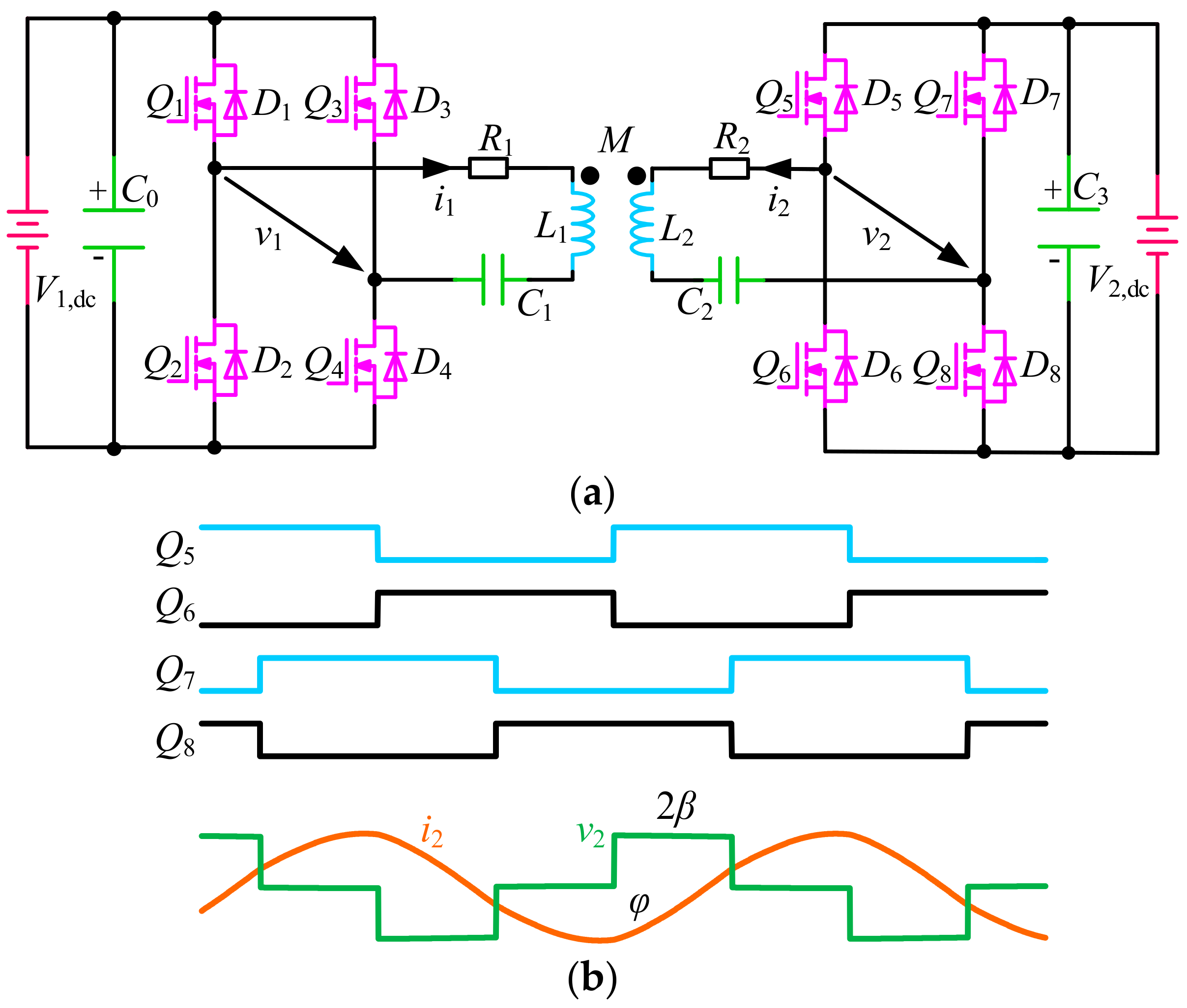
2. Modeling of WPT System

The schematic of the SS DAB WPT system is shown in Figure 1a. Since the SS topology consists of few resonant devices, it can reduce the cost, volume, and weight of the resonant network, which makes it widely adopted. V1,dc and V2,dc are the DC voltage sources. C0 and C3 are the filtering capacitors, whereas C1 and C2 are the primary and secondary compensation capacitors. Q1Q8 are the MOSFETs, and D1D8 are the diodes. The primary and secondary resonant voltages and currents are denoted as v1, v2, i1, and i2, respectively. The power can be transferred in both directions by controlling the phase difference between v1 and v2. L1 and L2 are the inductances of the transmitting and receiving coils whose parasitic resistances are R1 and R2, respectively.
According to the fundamental harmonic analysis and the circuit theory, the current loops of the primary and secondary sides can be obtained.
v 1 = i 1 ( R 1 + j ω L 1 + 1 j ω C 1 ) + j ω M i 2
v 2 = i 2 ( R 2 + j ω L 2 + 1 j ω C 2 ) + j ω M i 1
The ideal waveforms of the active bridge in the WPT system with zero dead time are shown in Figure 1b [13,15]. The phase angle of v2 is denoted as 2β, and v2 leads i2 by φ which can range from 0 to 360° in the DAB WPT system. The driving signals of the same phase leg are complementary to each other. Therefore, the dead time should be inserted to avoid short circuit in the experiments. However, the dead time can bring about some adverse effects. The following parts clearly elaborate the dead-time effect that may occur in the WPT systems.

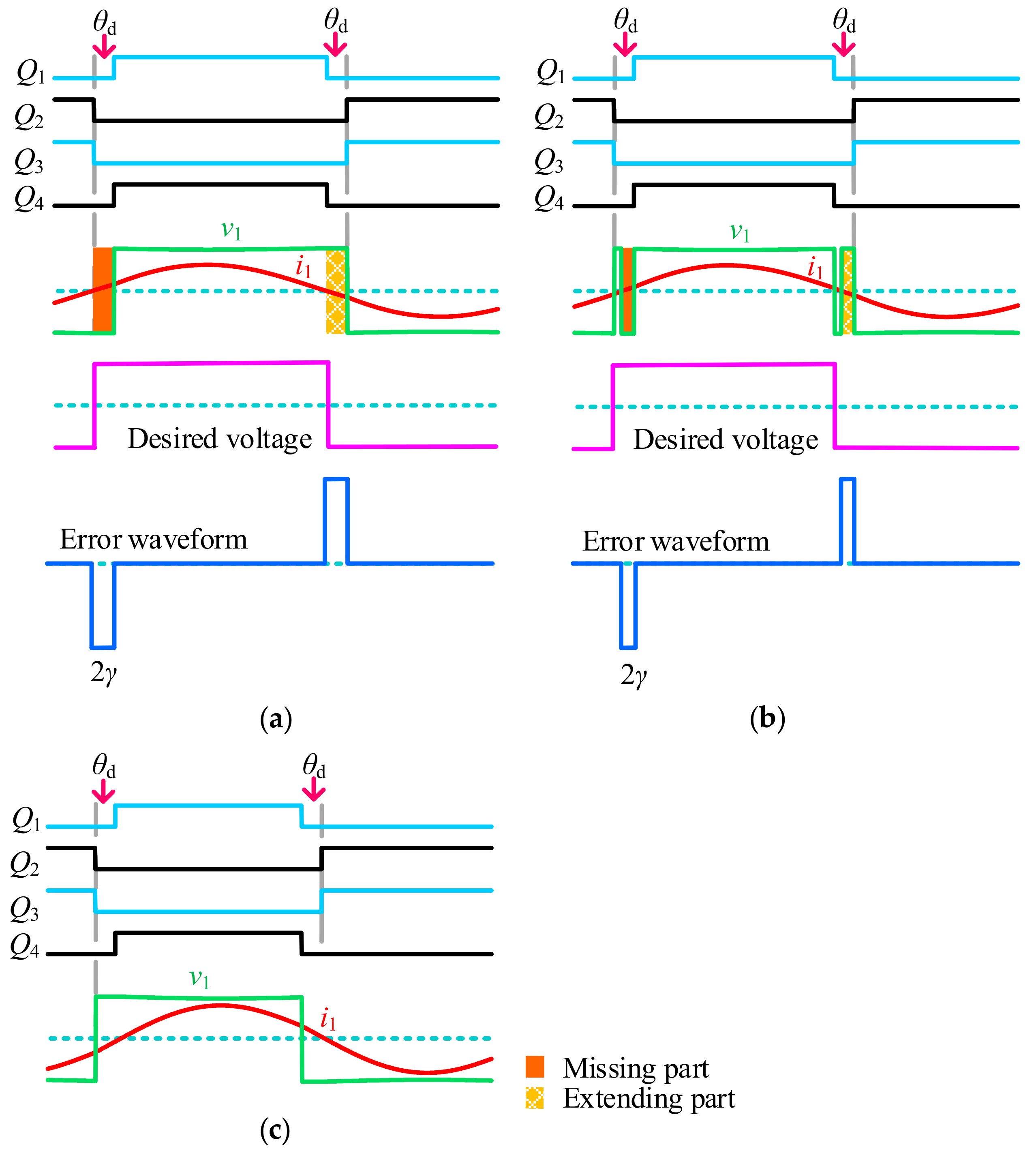
2.1. Dead-Time Effect of One Active Bridge WPT System

Primary active bridge and secondary diode bridge are adopted in most WPT systems, that is, only four diodes are used on the receiver side. The power is regulated by DC–DC converters, and the primary active bridge only functions as DC–AC conversion. The transmitter operates near the resonant point for high efficiency. Thus, there exist three operating modes of the primary active bridge. Figure 2 shows the three kinds of typical waveforms of the one active bridge WPT system with dead time Td, including the driving signals, the actual voltage and current, the desired voltage and the corresponding error waveform. θd corresponds to the phase angle during the dead time and 2γ presents the phase angle of the error waveform. The rising edge of the driving signal is delayed in order to obtain the required dead time, and v1 is expected to change when the driving signal is turned off. In Figure 2a, θd is inserted when i1 is positive. v1 becomes positive until Q1 is turned on, and it becomes negative until Q2 is turned on. The left part of v1 is missing, whereas the right part of v1 is extended. It is equivalent to shift v1 right by θd. In Figure 2b, θd is inserted during the zero-crossing point of i1. An error negative pulse and then an error positive pulse are produced, which has been observed in [19]. In Figure 2c, θd is inserted when i1 is negative. v1 becomes positive as soon as Q2 is turned off, and the desired waveform can be obtained. The driving signals are the same, whereas different output voltages appear when the zero-crossing point of i1 varies.
Although the dead-time effect has been investigated in the grid-tied inverters, it is significantly different in the resonant systems where the frequency of the output current becomes identical to the switching frequency. In order to evaluate the voltage distortion intuitively, the product of 2γ and the operating frequency f is defined as the voltage distortion ratio (VDR), and the maximum VDR (VDRmax) as shown in Figure 2a can be denoted as
VDR max = T d f × 100 % .
With the increase of the operating frequency, VDRmax increases quickly. In [27,28], the operating frequency of the VSI ranges from 20 kHz to 200 kHz, and the dead time ranges from 0.2 μs to 1.2 μs. In [29], the operating frequency of the commercial evaluation design kit can be up to 300 kHz, and the required dead time should be greater than 0.45 μs at 40 kHz. In [19], a double-side LCC WPT system operates at 95 kHz, where the adopted dead time is 0.5 μs. Therefore, Td is set at 0.5 μs in this paper. The operating frequency is 305 kHz in [30] and 515 kHz in [31], whose VDRmax values can be 15.25% and 25.75%, respectively. If without proper configuration of the dead time, the phase errors of [30,31] can be up to 54.9° and 92.7°, respectively.

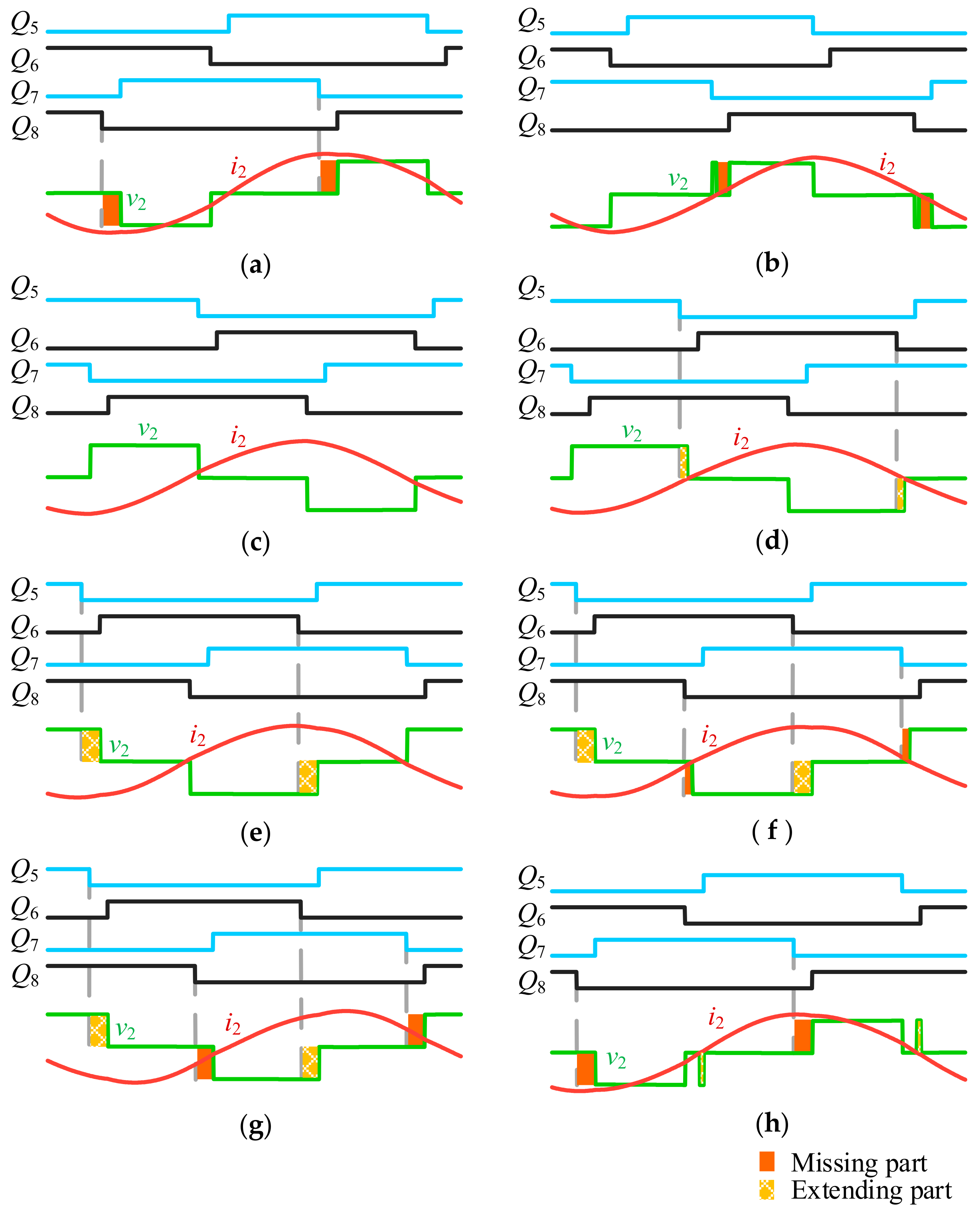
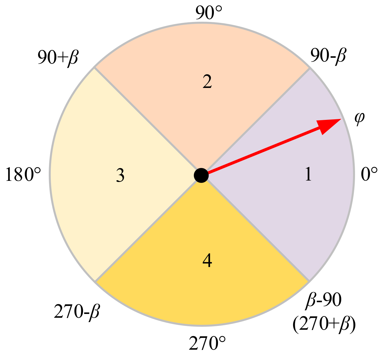
2.2. Dead-Time Effect of DAB WPT System

The active bridge analyzed in the Section 2.1 only acts as a DC/AC converter. It is a special case of phase control where the phase angle of v1 is 90°. Actually, the dead-time effect becomes more complex when applying the phase control, especially in the DAB WPT system.
Due to the symmetry of the DAB WPT system, the analysis and elimination of the dead-time effect can be fully investigated based on one active bridge. Since secondary phase angles are independent and controllable [14], the secondary active bridge is chosen as the research object in this paper, which benefits from the experimental validation of the analysis.
With the insertion of the dead time and the usage of multiple degrees of phase control, the operating conditions of the DAB WPT system can be classified into eight regions, as shown in Figure 3. In region 1, β − 90 + θd < φ < 90 − β. In region 2, 90 − β < φ < 90 − β + θd. In region 3, 90 − β + θd < φ < 90 + β. In region 4, 90 + β < φ < 90 + β + θd. In region 5, 90 + β + θd < φ < 270 − β. In region 6, 270 − β < φ < 270 − β + θd. In region 7, 270 − β + θd < φ < 270 + β. In region 8, 270 + β < φ < 270 + β + θd. When φ lies in the different regions, the dead-time effect varies.
The typical dead-time effect waveforms of the DAB WPT system in eight regions are shown in Figure 4. In Figure 4a, the left part of v2 is missing by θd, that is, β and φ are decreased by 0.5θd. In Figure 4b, the left part of v2 is missing, and the fault pulses are generated. It can be regarded as that a waveform with twice amplitude and reverse phase of the missing part is added to the expected waveform. In Figure 4c, the dead time has no influence on the generation of the desired v2. In Figure 4d, the right part of v2 is extended to the zero-crossing point of i2, which results in a greater β and a smaller φ. In Figure 4e, the right part of v2 is extended by θd. β is increased by 0.5θd, whereas φ is decreased by 0.5θd. In Figure 4f, the left part of v2 is missing, whereas the right part of v2 is extended by θd. The widths of the missing and the extending parts are different. Therefore, the error waveform consists of two periodical components. The total harmonic distortion can be calculated by using the superposition theorem twice. In Figure 4g, the left part of v2 is missing by θd, and the right part of v2 is extended by θd, which is equivalent to shift v2 right by θd. Thus, φ is reduced by θd. In Figure 4h, the left part of v2 is missing by θd, and a fault voltage pulse is produced as well. It is equivalent to adding two periodical error waveforms. Although the pulse widths of v2 in the eight figures are expected to be the same, the results can vary due to the dead-time effect.

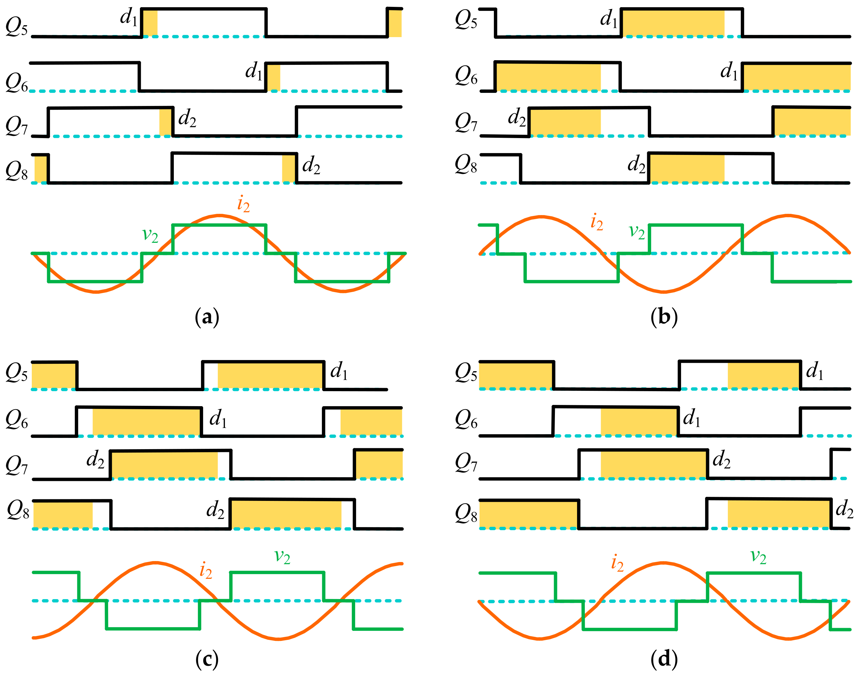
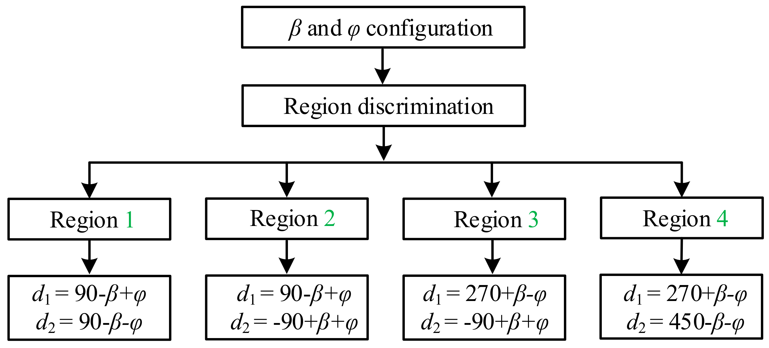
3. Dead-Time Elimination

As analyzed in the Section 2, the dead time has a great influence on the WPT systems. In this section, a novel PWM mode is presented, which is capable to remove the dead-time effect. The dead-time effect of the DAB WPT systems should be the most complex among all topologies, and their solutions can be easily applied to other resonant VSIs. Therefore, the proposed dead-time elimination method is analyzed based on the DAB WPT system.
The phase leg can be decomposed into two cells: the channel and the diode, as shown in Figure 5. iC and iD represent the currents flowing through the channel and the diode, respectively. i2 can flow through the channel of S6 or D6 at the positive period, and through the channel of S5 or D5 at the negative period. Despite the current direction, the freewheeling diode can provide a path for the current, which offers an opportunity for the dead-time elimination.
In the conventional DAB WPT systems, there are eight operating regions as shown in Figure 3. However, without considering the dead time, the operating conditions can be simplified into four regions according to the phase angles, which are shown in Figure 6. φ ranges from 0 to 360°, and β from 0 to 90°. In region 1, β − 90 < φ < 90 − β. In region 2, 90 − β < φ < 90 + β. In region 3, 90 + β < φ < 270 − β. In region 4, 270 − β < φ < 270 + β. When φ is greater than 270 + β, it is denoted as a negative value, which belongs to region 1. During different operating regions, the system has different freewheeling paths of the resonant current. Therefore, dead-time elimination characteristic varies in four different regions.
The typical waveforms of the corresponding four regions are shown in Figure 7, where d1 and d2 are the lengths of the shadow areas. It is recognized that the states of the shadow areas cannot affect the generation of v2, where the current can freewheel through the diodes. Dead-time elimination of the DAB WPT system can be achieved by turning off the shadow area signals. Furthermore, the lengths of d1 and d2 can be obtained according to the following derivations.
Region 1:
φ belongs to (β − 90, 90 − β), as shown in Figure 7a. Q5 and Q6 must be turned on after Q6 and Q5 are turned off respectively, providing d1 length. However, Q7 and Q8 must be turned off before Q8 and Q7 are turned on respectively, providing d2 length. The lengths of d1 and d2 are
d 1 = 90 β + φ ,
d 2 = 90 β φ .
Region 2:
φ belongs to (90 − β, 90 + β), as shown in Figure 7b. Q5 and Q6 must be turned on after Q6 and Q5 are turned off respectively, providing d1 length. Same operations are implemented on Q7 and Q8, providing d2 length. The lengths of d1 and d2 are
d 1 = 90 β + φ ,
d 2 = 90 + β + φ .
Region 3:
φ belongs to (90 + β, 270 − β), as shown in Figure 7c. Q5 and Q6 must be turned off before Q6 and Q5 are turned on respectively, providing d1 length. However, Q7 and Q8 must be turned on after Q8 and Q7 are turned off respectively, providing d2 length. The lengths of d1 and d2 are
d 1 = 270 + β φ ,
d 2 = 90 + β + φ .
Region 4:
φ belongs to (270 − β, 270 + β), as shown in Figure 7d. Q5 and Q6 must be turned off before Q6 and Q5 are turned on respectively, providing d1 length. Same operations are implemented on Q7 and Q8, providing d2 length. The lengths of d1 and d2 are
d 1 = 270 + β φ ,
d 2 = 450 β φ .
The PWM mode in the proposed method provides an available time for current freewheeling without affecting neither β nor φ. However, as in the borders mentioned above, two special cases should be noticed. One is the border between region 1 and region 2 where d2 becomes 0, as can be indicted by (5). The other is the border between region 1 and region 4 where d1 becomes 0, as can be indicted by (4). Therefore, it is recommended not to operate near these two borders. If necessary, dead time should be added between the complementary driving signals.
The flowchart of the calculation of d1 and d2 is shown in Figure 8. First, configure the value of β and φ. Then, discriminate the corresponding phase region. Afterwards, calculate the values of d1 and d2 according to (4)–(11). Finally, the corresponding compared values of the reserved registers of the controller are reconfigured based on the region, β, φ, d1, and d2, which generates the desired driving signals. Since the proposed modulation varies with four regions as analyzed in Figure 7, four compared value calculation functions are provided in the program. If the system needs to transit from one region to another, recalculate the compared values according to the corresponding function and reload them into the reserved registers.

4. Simulations and Experiments

To verify the feasibility and effectiveness of the proposed method, a simulation model in MATLAB/Simulink (R2017a, MathWorks, Natick, MA, USA) and a prototype system have been built. The prototype photograph of the system is shown in Figure 9, whose parameters are listed in Table 1. According to SAE J2954 [32], the operating frequency must remain in the range of 81.38 kHz to 90 kHz. In this paper, the operating frequency is set at 90 kHz, where the dead-time effect is more obvious. The primary and secondary active bridges consist of four half bridges where eight C2M0080120D MOSFETs and eight C4D20120D diodes are used. The primary and secondary DC voltages are connected, and the voltage source only needs to supply the power losses of the system, which is widely adopted in the test of the DAB systems. Both the primary and secondary compensation capacitors are made up of two 0.1 μF AC capacitors in series. The inner and outer radii of the coils are 16 cm and 19 cm, respectively. Two magnetic core layers are utilized to shield the magnetic field and increase the mutual inductance. The air gap (d) between the transmitting and receiving coils is 10 cm with a mutual inductance of 14 μH measured by LCR meter TH2830. The waveforms are observed and recorded by Tektronix TPS2024B (Tektronix, Beaverton, OR, USA).

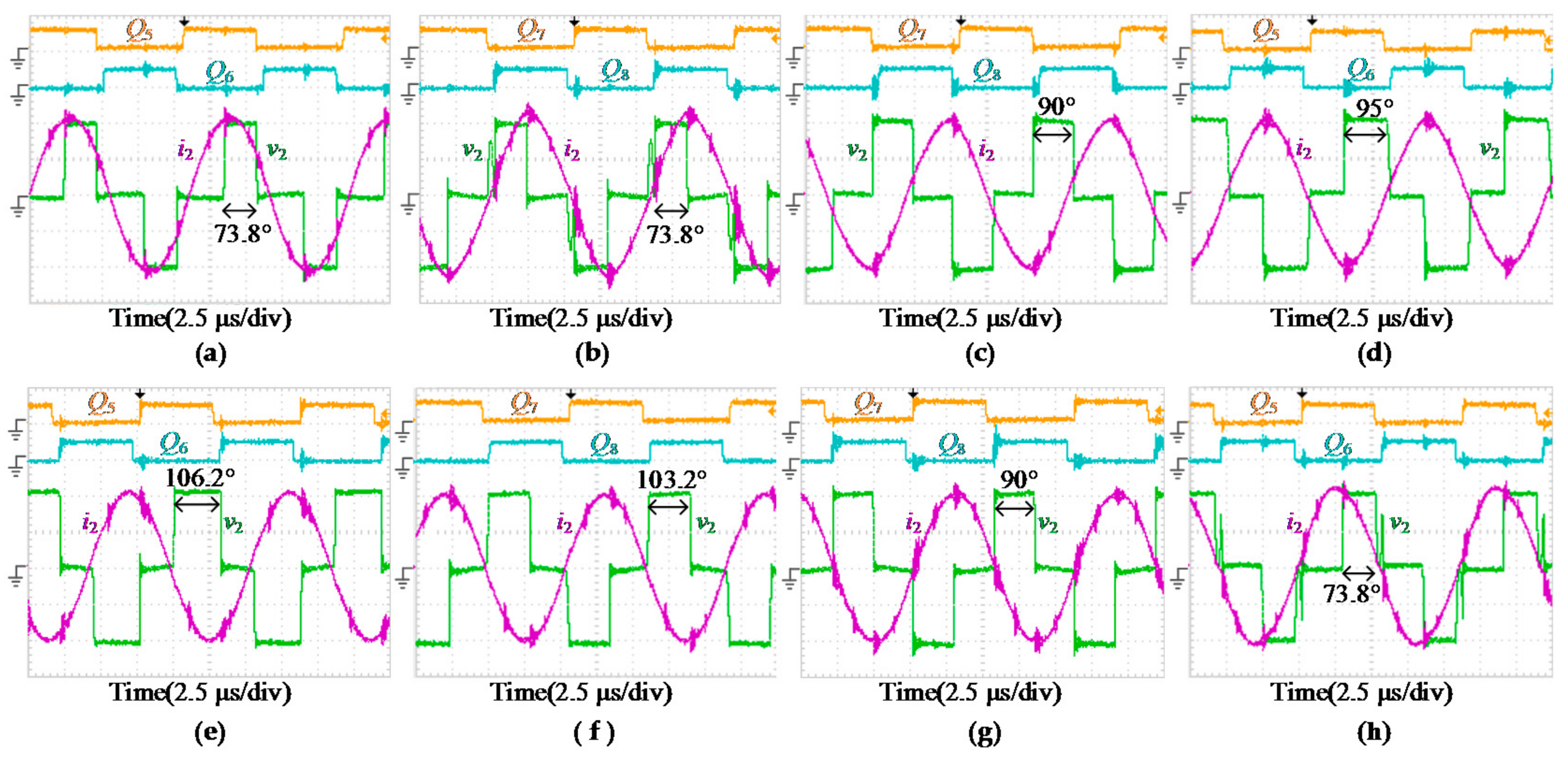
4.1. Dead-Time Effect

Figure 10 and Figure 11 show the simulated and experimental results of the eight kinds of dead-time effect in the DAB WPT system, where the dead time is set at 0.5 μs. The given β is 45°. According to Equation (3), the value of VDRmax of this system is 4.5%, corresponding to 16.2° phase error. Due to limited channels of the oscilloscope, different experimental driving signals are selected to display for better judgement of the region. In Figure 10a and Figure 11a, the given φ is 335°, and the zero-crossing point of i2 falls into region 1. The left part of v2 is missing by 16.2°, that is, the actual φ and β become 326.9° and 36.9°, respectively. In Figure 10b and Figure 11b, φ is 47°, and the zero-crossing point of i2 falls into region 2 (within the dead time). The left part of v2 is missing, which results in the appearance of the error pulse voltage. Since the pulse width is small and the voltage changes slowly during the zero-crossing point of i2, the experimental v2 decreases before reaching the peak. φ and β become 38.9° and 36.9°, respectively. In Figure 10c and Figure 11c, φ is 120°, and the zero-crossing point of i2 falls into region 3. The dead time does not affect the generation of v2. In Figure 10d and Figure 11d, the given φ is 140°, and the zero-crossing point of i2 falls into region 4 (within the dead time). The right part of v2 is extended to the zero-crossing point of i2, where v2 changes its state slowly in the experiment. φ and β become 137.5° and 47.5°, respectively. In Figure 10e and Figure 11e, the given φ is 210°, and the zero-crossing point of i2 falls into region 5. The right part of v2 is extended by 16.2°, i.e., φ and β become 201.9° and 53.1°, respectively. In Figure 10f and Figure 11f, the given φ is 228°, and the zero-crossing point of i2 falls into region 6 (within the dead time). The left part of v2 is missing until the zero-crossing point of i2, whereas the right part of v2 is extended by 16.2°. φ and β become 218.4° and 51.6°, respectively. In Figure 10g and Figure 11g, the given φ is 238°, and the zero-crossing point of i2 falls into region 7. The left part of v2 is missing by 16.2°, whereas the right part is extended by 16.2°. Therefore, φ becomes 221.8°, and β remains unchanged. It is equivalent to shift v2 right by 16.2°. In Figure 10h and Figure 11h, the given φ is 319°, and the zero-crossing point of i2 falls into region 8 (within the dead time). The left part of v2 is missing by 16.2°, along with a fault pulse voltage. φ and β become 310.9° and 36.9°, respectively. The simulated and experimental results agree well with the analysis in Section 2.
As evident from the simulated and experimental illustrations, the system can operate as desired only in the region 3, in comparison with the eight operating regions, when inserting the dead time. Moreover, the voltage reverses thrice within a short time during the region 2 and the region 8, which can damage the semiconductors. Therefore, the dead-time effect in the DAB WPT system becomes problematic, and it should be addressed well in the practical applications.

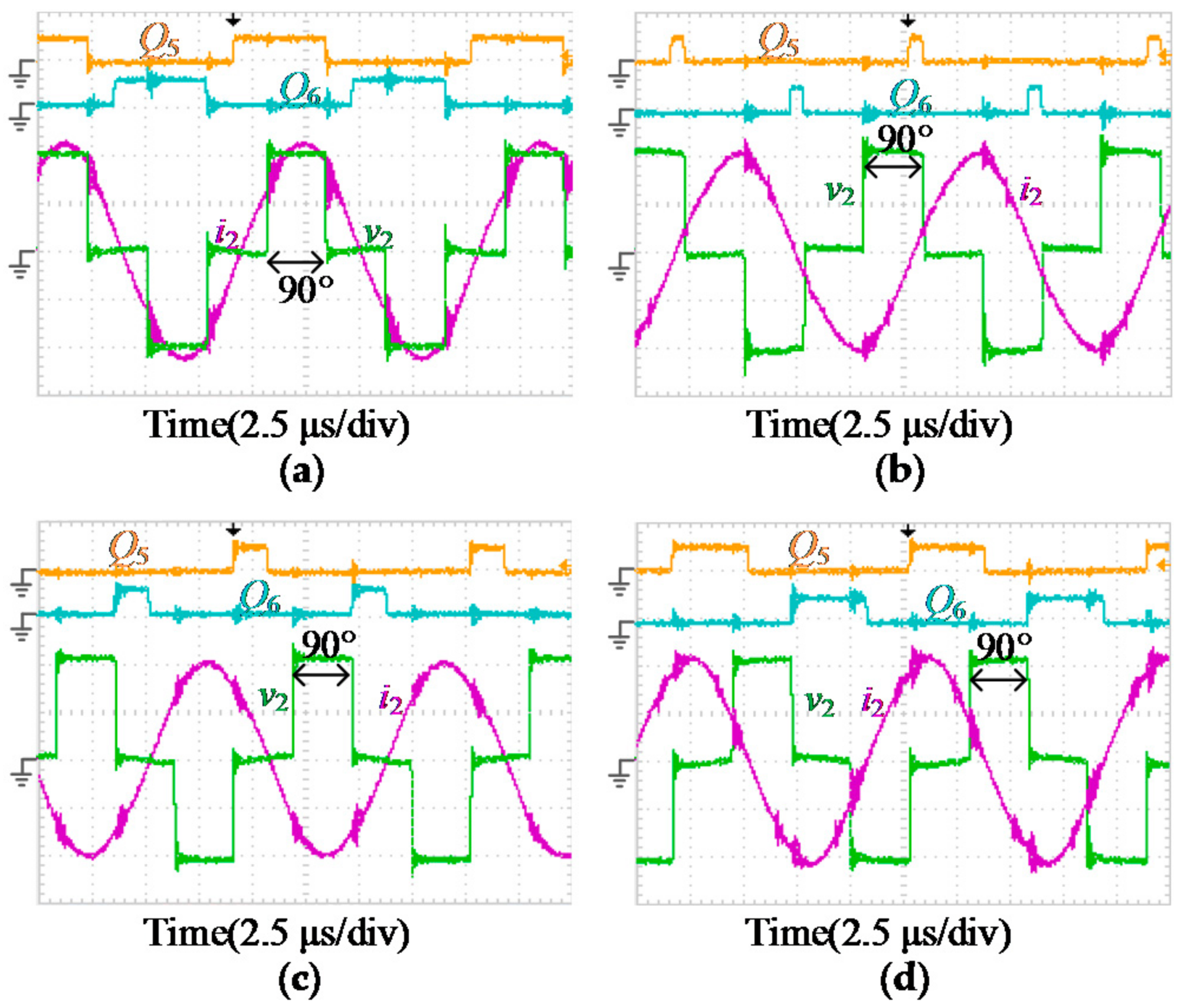
4.2. Dead-Time Elimination

Figure 12 and Figure 13 show the simulated and experimental results of the dead-time elimination in the reclassified four regions. To avoid the incorrect operation, 5° phase redundancy is adopted, i.e., the actual d1 and d2 are 5° smaller than the calculated values. In Figure 12a and Figure 13a, φ is 0°, and the zero-crossing point of i2 falls into region 1. Both d1 and d2 are 40°. In Figure 12b and Figure 13b, φ is 120°, and the zero-crossing point of i2 falls into region 2. d1 and d2 are 160° and 70°, respectively. Thus, the lengths of the valid voltages of Q5 and Q6 are only 20°. In Figure 12c and Figure 13c, φ is 180°, and the zero-crossing point of i2 falls into region 3. Both d1 and d2 are 130°. In Figure 12d and Figure 13d, φ is 245°, and the zero-crossing point of i2 falls into region 4. d1 and d2 are 65° and 155°, respectively. The actual β and φ are equal to the given values in the four regions. The transmitting DC power of the simulations reaches 541 W with 92.1% DC–DC efficiency, as shown in Figure 12c. The transmitting DC power of the experiments reaches 645 W with 88.7% DC–DC efficiency, as shown in Figure 13c.
In the proposed PWM mode, the driving signals of the same phase leg are no longer complementary to each other, and consequently, the dead time is not necessary. The desired output voltage can be generated in all the regions. The simulated and experimental results validate the feasibility and effectiveness of the proposed dead-time elimination method.
In order to demonstrate the validity of the analysis, d1 and d2 are designed as large as possible in this paper. In practice, d1 and d2 can be adjusted based on the specific operating conditions, and ensure the current flowing through the channel as long as possible, which can reduce the conduction losses.

4.3. Comparisons and Discussions

The differences between the expected and the actual phase angles (Δβ and Δφ) of conventional PWM mode and proposed PWM mode are shown in Table 2. In the conventional PWM mode, the dead time is inserted. Δβ can increase or decrease in the different regions, whereas Δφ can only decrease. The maximum positive Δβ is 8.1° appearing in region 5, whereas the maximum negative Δβ is −8.1° appearing in region 1, region 2, and region 8. The maximum negative Δφ can be up to −16.2°, appearing in region 7. Δβ and Δφ are 0° only in region 3. In the proposed PWM mode, dead-time elimination is achieved, and the phase errors are 0° in all the regions. In [11,12,13,14], β and φ are used to realize the impedance matching for maximum efficiency point tracking. The phase errors between the given and the actual values can result in control performance deterioration. Furthermore, it can affect the transferred power and generate undesired harmonics.
Although solutions of dead-time effect have been investigated in the low output current frequency applications [18,20,21,22,23,24,25,26], they cannot be applied to the WPT systems where the output current frequency is identical to the switching frequency. The researchers in [19] realize the significant influence of the dead time on the WPT systems, and derive the optimal dead time based on one condition. Although the dead time is a common issue of VSIs, a very few literature studies comprehensively discuss its effects in the WPT systems and explore the elimination methods. As evident from the simulated and experimental results, the proposed technique can effectively control the dead-time effect of the WPT systems up to a certain extent, which contributes to the realization of flexible power conversion. In addition, the proposed method is not influenced by the system parameters. Generally, only high performance and expensive semiconductor devices with short rise and fall times can operate at a high frequency. However, by employing the proposed dead-time elimination method, the freewheeling period can be fully utilized as shown in Figure 12 and Figure 13, and common semiconductor devices can work at a higher frequency in the resonant systems, which can reduce the cost.

5. Conclusions

This paper investigates the possible dead-time effect of the WPT systems and presents a novel dead-time elimination method based on the SS DAB topology. Considering the dead time, the operating conditions of the DAB WPT system can be divided into eight regions. However, the system can operate properly only in one region, and different voltage distortions appear in the other seven regions. Maximum phase error can be up to 16.2° at 90 kHz with 0.5 μs dead time. By utilizing the freewheeling diode, some states of the driving signals cannot affect the resonant voltages, and they can be turned off for dead-time elimination. Without considering the dead time, the DAB WPT system can be reclassified into four operating regions, and the expressions of the lengths of the inessential driving signals are derived. Through the proposed PWM mode, the desired waveform can be generated correctly in all four regions. A simulation and a prototype with over 500 W transmitting power are established, and the results validate the efficacy of the proposed analysis.

Author Contributions

X.L. proposed the main idea, designed and performed the experiments, and wrote the manuscript. T.W. and N.J. double-checked and discussed the results and the whole manuscript. S.H. and M.A. helped to modify the manuscript. X.Y. and H.T. contributed to the discussion of this study. All authors have approved the final version of this manuscript.

Funding

This research was funded by United Foundation of NSFC-Henan grant number U1604136.

Acknowledgments

The authors acknowledge support from United Foundation of NSFC-Henan grant U1604136.

Conflicts of Interest

The authors declare no conflict of interest.

References

  1. Kim, T.-H.; Yoon, S.; Yook, J.-G.; Yun, G.-H.; Lee, W.Y. Evaluation of power transfer efficiency with ferrite sheets in WPT system. In Proceedings of the 2017 IEEE Wireless Power Transfer Conference (WPTC), Taipei, Taiwan, 10–12 May 2017. [Google Scholar]
  2. Kim, T.-H.; Yun, G.-H.; Lee, W.Y.; Yook, J.-G. Asymmetric Coil Structures for Highly Efficient Wireless Power Transfer Systems. IEEE Trans. Microw. Theory Technol. 2018. [Google Scholar] [CrossRef]
  3. Tsiropoulou, E.E.; Mitsis, G.; Papavassiliou, S. Interest-aware Energy Collection & Resource Management in Machine to Machine Communications. Ad Hoc Netw. 2018, 68, 48–57. [Google Scholar]
  4. Vamvakas, P.; Tsiropoulou, E.E.; Vomvas, M.; Papavassiliou, S. Adaptive Power Management in Wireless Powered Communication Networks: A User-Centric Approach. In Proceedings of the 38th IEEE Sarnoff Symposium, Newark, NJ, USA, 8–20 Septemner 2017. [Google Scholar]
  5. Bashirullah, R. Wireless implants. IEEE Microw. Mag. 2010, 11, S14–S23. [Google Scholar] [CrossRef]
  6. Lu, Y.; Ma, D.B. Wireless Power Transfer System Architectures for Portable or Implantable Applications. Energies 2016, 9, 1087. [Google Scholar] [CrossRef]
  7. Wang, Z.; Wei, X.; Dai, H. Design and Control of a 3 kW Wireless Power Transfer System for Electric Vehicles. Energies 2016, 9, 10. [Google Scholar] [CrossRef]
  8. Lee, S.-H.; Kim, J.-H.; Lee, J.-H. Development of a 60 kHz, 180 kW, Over 85% Efficiency Inductive Power Transfer System for a Tram. Energies 2016, 9, 1075. [Google Scholar] [CrossRef]
  9. Cochran, S.; Quaiyum, F.; Fathy, A.; Cosniett, D.; Yang, S. A GaN-based Synchronous Rectifier for WPT Receivers with Reduced THD. In Proceedings of the 2016 IEEE PELS Workshop on Emerging Technologies: Wireless Power Transfer (WoW), Knoxville, TN, USA, 4–6 October 2016; pp. 81–87. [Google Scholar]
  10. Diekhans, T.; De Doncker, R.W. A dual-side controlled inductive power transfer system optimized for large coupling factor variations and partial load. IEEE Trans. Power Electron. 2015, 30, 6320–6328. [Google Scholar] [CrossRef]
  11. Berger, A.; Agostinelli, M.; Vesti, S.; Oliver, J.A.; Cobos, J.A.; Huemer, M. Phase-shift and amplitude control for an active rectifier to maximize the efficiency and extracted power of a wireless power transfer system. In Proceedings of the 2015 IEEE Applied Power Electronics Conference and Exposition (APEC), Charlotte, NC, USA, 15–19 March 2015; pp. 1620–1624. [Google Scholar]
  12. Berger, A.; Agostinelli, M.; Vesti, S.; Oliver, J.A.; Cobos, J.A.; Huemer, M. A Wireless Charging System Applying Phase-Shift and Amplitude Control to Maximize Efficiency and Extractable Power. IEEE Trans. Power Electron. 2015, 30, 6338–6348. [Google Scholar] [CrossRef]
  13. Mai, R.; Liu, Y.; Li, Y.; Yue, P.; Cao, G.; He, Z. An Active Rectifier Based Maximum Efficiency Tracking Method Using an Additional Measurement Coil for Wireless Power Transfer. IEEE Trans. Power Electron. 2017, 33, 716–728. [Google Scholar] [CrossRef]
  14. Liu, X.; Wang, T.; Yang, X.; Jin, N.; Tang, H. Analysis and Design of a Wireless Power Transfer System with Dual Active Bridges. Energies 2017, 10, 1588. [Google Scholar] [CrossRef]
  15. Bac, X.N.; Vilathgamuwa, D.M.; Foo, G.H.B.; Wang, P.; Ong, A.; Madawala, U.K.; Trong, D.N. An Efficiency Optimization Scheme for Bidirectional Inductive Power Transfer Systems. IEEE Trans. Power Electron. 2015, 30, 6310–6319. [Google Scholar]
  16. Thrimawithana, D.J.; Madawala, U.K.; Neath, M. A Synchronization Technique for Bidirectional IPT Systems. IEEE Trans. Ind. Electron. 2013, 60, 301–309. [Google Scholar] [CrossRef]
  17. Tang, Y.; Chen, Y.; Madawala, U.K.; Thrimawithana, D.J.; Ma, H. A New Controller for Bi-directional Wireless Power Transfer Systems. IEEE Trans. Power Electron. 2017. [Google Scholar] [CrossRef]
  18. Zhang, Z.; Wang, F.; Costinett, D.J.; Tolbert, L.M. Dead-time optimization of SiC devices for voltage source converter. In Proceedings of the 2015 IEEE Applied Power Electronics Conference and Exposition (APEC), Charlotte, NC, USA, 15–19 March 2015; pp. 1145–1152. [Google Scholar]
  19. Zhang, X.; Lai, Z.; Xiong, R.; Li, Z.; Zhang, Z.; Song, L. Switching Device Dead Time Optimization of Resonant Double-Sided LCC Wireless Charging System for Electric Vehicles. Energies 2017, 10, 1772. [Google Scholar] [CrossRef]
  20. Attaianese, C.; Nardi, V.; Tomasso, G. A novel SVM strategy for VSI dead-time-effect reduction. IEEE Trans. Ind. Appl. 2015, 41, 1667–1674. [Google Scholar] [CrossRef]
  21. Choi, J.S.; Yoo, J.Y.; Lim, S.W.; Kim, Y.S. A novel dead time minimization algorithm of the PWM inverter. In Proceedings of the 1999 IEEE Industry Applications Conference (Thirty-Forth IAS Annual Meeting), Phoenix, AZ, USA, 3–7 October 1999; Volume 4, pp. 2188–2193. [Google Scholar]
  22. Urasaki, N.; Senjyu, T.; Uezato, K.; Funabashi, T. An adaptive dead-time compensation strategy for voltage source inverter fed motor drives. IEEE Trans. Power Electron. 2005, 20, 1150–1160. [Google Scholar] [CrossRef]
  23. Patel, P.J.; Patel, V.; Tekwani, P.N. Pulse-based dead-time compensation method for self-balancing space vector pulse width-modulated scheme used in a three-level inverter-fed induction motor drive. IET Power Electron. 2011, 4, 624–631. [Google Scholar] [CrossRef]
  24. Chen, L.; Peng, F.Z. Dead-time elimination for voltage source inverters. IEEE Trans. Power Electron. 2008, 23, 574–580. [Google Scholar] [CrossRef]
  25. Wang, Y.; Gao, Q.; Cai, X. Mixed PWM for Dead-Time Elimination and Compensation in a Grid-Tied Inverter. IEEE Trans. Ind. Electron. 2011, 58, 4797–4803. [Google Scholar] [CrossRef]
  26. Lin, Y.K.; Lai, Y.S. Dead-time elimination of PWM-controlled inverter/converter without separate power sources for current polarity detection circuit. IEEE Trans. Ind. Electron. 2009, 56, 2121–2127. [Google Scholar]
  27. Yin, S.; Tseng, K.J.; Tong, C.F.; Simanjorang, R.; Gajanayake, C.J.; Gupta, A.K. A 99% efficiency SiC three-phase inverter using synchronous rectification. In Proceedings of the 2016 IEEE Applied Power Electronics Conference and Exposition (APEC), Long Beach, CA, USA, 20–24 March 2016; pp. 2942–2949. [Google Scholar]
  28. Yin, S.; Liu, Y.; Liu, Y.; Tseng, K.J.; Pou, J.; Simanjorang, R. Comparison of SiC Voltage Source Inverters Using Synchronous Rectification and Freewheeling Diode. IEEE Trans. Power Electron. 2018, 65, 1051–1061. [Google Scholar] [CrossRef]
  29. Cree Inc. KIT8020CRD8FF1217P-1 CREE Silicon Carbide MOSFET Evaluation Kit User’s Manual; Cree Inc.: Durham, NC, USA, 2014. [Google Scholar]
  30. Ahn, D.; Kim, S.; Moon, J.; Cho, I.K. Wireless Power Transfer with Automatic Feedback Control of Load Resistance Transformation. IEEE Trans. Power Electron. 2016, 31, 7876–7886. [Google Scholar] [CrossRef]
  31. Li, H.; Li, J.; Wang, K.; Chen, W.; Yang, X. A maximum efficiency point tracking control scheme for wireless power transfer systems using magnetic resonant coupling. IEEE Trans. Power Electron. 2015, 30, 3998–4008. [Google Scholar] [CrossRef]
  32. J2954™ NOV2017, SAE J2954. 2017. Available online: https://saemobilus.sae.org/content/J2954_201711 (accessed on 14 June 2018).
Figure 1. Dual active bridge (DAB) wireless power transfer (WPT) system. (a) System schematic; (b) Ideal waveforms with zero dead time.
Energies 11 01577 g001
Figure 2. Dead-time effect of one active bridge WPT system. (a) Dead time is inserted when i1 > 0; (b) Dead time is inserted during the zero-crossing point of i1; (c) Dead time is inserted when i1 < 0.
Energies 11 01577 g002
Figure 3. Operating regions of DAB WPT system with dead time.
Energies 11 01577 g003
Figure 4. Dead-time effect of the DAB WPT system where the orange and yellow areas present the missing and extending parts of the voltage, respectively. (a) Region 1; (b) Region 2; (c) Region 3; (d) Region 4; (e) Region 5; (f) Region 6; (g) Region 7; (h) Region 8.
Energies 11 01577 g004
Figure 5. Decomposition of a phase leg. (a) i2 > 0; (b) i2 < 0.
Energies 11 01577 g005
Figure 6. Operating regions of the DAB WPT system without dead time.
Energies 11 01577 g006
Figure 7. Dead-time elimination regions in the DAB WPT system where the driving signal in the shadow areas can be turned off. (a) Region 1; (b) Region 2; (c) Region 3; (d) Region 4.
Energies 11 01577 g007
Figure 8. Calculation of d1 and d2.
Energies 11 01577 g008
Figure 9. Prototype photograph of the DAB WPT system.
Energies 11 01577 g009
Figure 10. Simulated results of the eight kinds of dead-time effect in the DAB WPT system. (a) Region 1; (b) Region 2; (c) Region 3; (d) Region 4; (e) Region 5; (f) Region 6; (g) Region 7; (h) Region 8. i2: 5 A/div; v2: 50 V/div.
Energies 11 01577 g010
Figure 11. Experimental results of the eight kinds of dead-time effect in the DAB WPT system. (a) Region 1; (b) Region 2; (c) Region 3; (d) Region 4; (e) Region 5; (f) Region 6; (g) Region 7; (h) Region 8. Q5Q8: 5 V/div; i2: 5 A/div; v2: 50 V/div.
Energies 11 01577 g011
Figure 12. Simulated results of proposed dead-time elimination method. (a) Region 1; (b) Region 2; (c) Region 3; (d) Region 4. i2: 5 A/div; v2: 50 V/div.
Energies 11 01577 g012
Figure 13. Experimental results of proposed dead-time elimination method. (a) Region 1; (b) Region 2; (c) Region 3; (d) Region 4. Q5Q8: 5 V/div; i2: 5 A/div; v2: 50 V/div.
Energies 11 01577 g013
Table 1. Key parameters of the proposed system.
SymbolParameterValue
V1,dcprimary DC voltage100 V
V2,dcsecondary DC voltage100 V
L1transmitter coil inductance61 μH
C1transmitter compensation capacitance0.05 μF
L2receiver coil inductance61 μH
C2receiver compensation capacitance0.05 μF
finverter frequency90 kHz
dthe air gap between the coils10 cm
Mmutual inductance14 μH
Table 2. Comparisons between conventional and proposed PWM modes.
PWM ModesRegionsΔβΔφ
Conventional PWM modeRegion 1−8.1°−8.1°
Region 2−8.1°−8.1°
Region 3
Region 42.5°−2.5°
Region 58.1°−8.1°
Region 66.6°−9.6°
Region 7−16.2°
Region 8−8.1°−8.1°
Proposed PWM modeRegion 1
Region 2
Region 3
Region 4

