1. Introduction
With the explosion of mobility devices, the momentum towards IoT and wearable devices is an obvious and predicted trend. Even so, the development of energy and battery supply is still far from the demand for IoT/wearable devices currently. That said, the demand for an external power source supporting wireless charging technology is high. For wearable devices, charging them through a Radio Frequency (RF) energy harvesting system is the best solution, and this is the target of all other future devices [
1,
2,
3]. In RF energy harvesting system, the power transfer efficiency depends on the transfer environment, and the distance between the receiver and the RF power source [
4,
5,
6]. These factors are unavoidable. The only way to improve the power transfer efficiency from the source to the devices is to have an extremely high power conversion efficiency receiver. The RF wireless power received at the output of the antenna is collected by a rectifier. The output voltage of the rectifier is not constant, and varies over a wide range, due to the unfixed receiver power at the antenna. The voltage regulator must be able to operate over a wide input voltage range, and provide ripple-less output voltage. The buck-boost direct current to direct current (DC–DC) converter is a good choice for this specification [
7,
8]. Creating a DC–DC converter that can operate with a wide voltage variation range of rectifier will expand the application of RF energy harvesting system to more electronics device types.
When the input voltage varies from very low to very high values, it crosses over the desired output voltage. When the input is lower than the desired output, the converter operates as a boost converter. When the input is higher than the desired output, the converter operates as a buck converter. The converter operates in buck-boost mode when the input voltage is close to, or equal to the desired output. The DC–DC converter is required to maintain constantly high power conversion efficiency with all the three modes of buck, boost, and buck-boost. The common structure for the buck-boost converter is the interleaved technique [
9,
10,
11], where a number of converter sets are integrated into one. The benefit of the interleaved technique is to release the stress on the switch devices, and to obtain a high-power density converter. By integrating many pairs of converter sets, the phase offset control and multiple internal oscillator increase the stress on the controller. Therefore, the problem of non-smoothness and discontinuity occurs in the converter. Other techniques are capable of providing buck-boost operation, such as the inverting buck-boost [
12,
13]. However, the constantly high switching current of the buck-boost operation places great stress on the devices. The non-inverting buck-boost converter combines buck-switches and boost-switches in one circuit, and they share a common inductance [
14,
15,
16]. This structure releases the stress in the switching components and the target of wide input voltage range can be achieved. Nevertheless, due to the two independently controllable switching sets, the controller for this non-inverting converter is very hard to obtain high conversion efficiency. Reference [
14] presents a buck-boost DC–DC converter with excluding the buck-boost mode. The operation of the converter jumps between buck and boost mode may cause a large ripple in the output voltage. The scalable driver and power stage are proposed in [
15]. By doing that, the size of the power transistor is adjusted based on the load condition instead of the pulse-width modulation and the pulse-skip modes as in ordinary DC–DC converter. This approach reduces the unwanted ripple of that output but it may lead to the high leakage current at the transistors disabled during the light load current mode. This reduces the efficiency of the proposed buck-boost converter. In reference [
16], a zero-voltage-switching technique is proposed to implement the buck-boost converter. Two pairs of small auxiliary inductor and capacitor are used to obtain the zero-voltage-switching under the different load currents without increasing the voltage stress across the power transistors. This approach requires the special Metal-Oxide Semiconductor Field-Effect Transistor (MOSFET) devices structure (eGaNs) and large inductance and capacitance value. Another approach to implementing the buck-boost converter based on the digital control is proposed in [
13]. The proposed digital-control-based buck-boost converter operates with light load condition at discontinuous conduction mode. For a full application, this structure needs to be improved more in terms of operational efficiency and capability at higher load current condition. Another approach based on digital control to implement non-inverting buck-boost DC–DC converter is presented in [
17]. The proposed non-inverting buck-boost DC–DC converter operates by switching between buck and boost mode. The author proposes the duty-cycle-overlap control technique to reduce the unstable output voltage and an unpredictable output voltage ripple. However, the efficiency of the proposed structure needs to be improved.
In this paper, we apply the non-inverting DC–DC converter to adapt to wide input voltage variation. The controller is simplified, but the converter maintains high conversion efficiency [
18,
19]. To achieve smooth conversion, the buck, buck-boost, and boost mode selection must constantly occur rapidly with zero delay. The mode selector detects the input voltage and decides the operational mode. Our mode selector adapts immediately after detecting the change at the input with ultra-low delay. The delay between the change detected and the mode selection of our design can be approximated as zero. The input of the DC–DC converter contains an extremely large fluctuations of voltage and current due to the energy harvesting application. That may cause the unstable mode selection [
20] and lead to unexpected ripple at the output voltage. To eliminate the unstable mode selection, we proposed hysteresis mode selection method to improve the output ripple. The input fluctuations also cause the dead stage of pulse width modulation (PWM), thus we also introduced the Min-Max Duty Generator to improve the feedback control by providing a quick response and protection to input and output change. A single PWM signal generator and single saw-tooth signal generator are used in the converter to eliminate the phase mismatch and regulation discontinuity. A new logic control block is introduced, and the mode selector is combined with the signal PWM to synchronize the switching of four power transistors and provide the best regulating output at the highest efficiency. To reduce the inrush current at the initial state of the operation, the output soft start-up circuit is implemented to reduce the voltage gap between the input and the output at the initial stage of operation. The gate control voltage is also optimized to avoid leakage, and turn the transistor on when the drain voltage varies over a wide range.
The rest of this paper is organized as follows:
Section 2 presents the proposed architecture of the buck-boost DC–DC converter.
Section 3 shows the experimental results of testing of the manufactured DC–DC converter.
Section 4 concludes the paper.
2. Architecture of the Buck-Boost DC–DC Converter
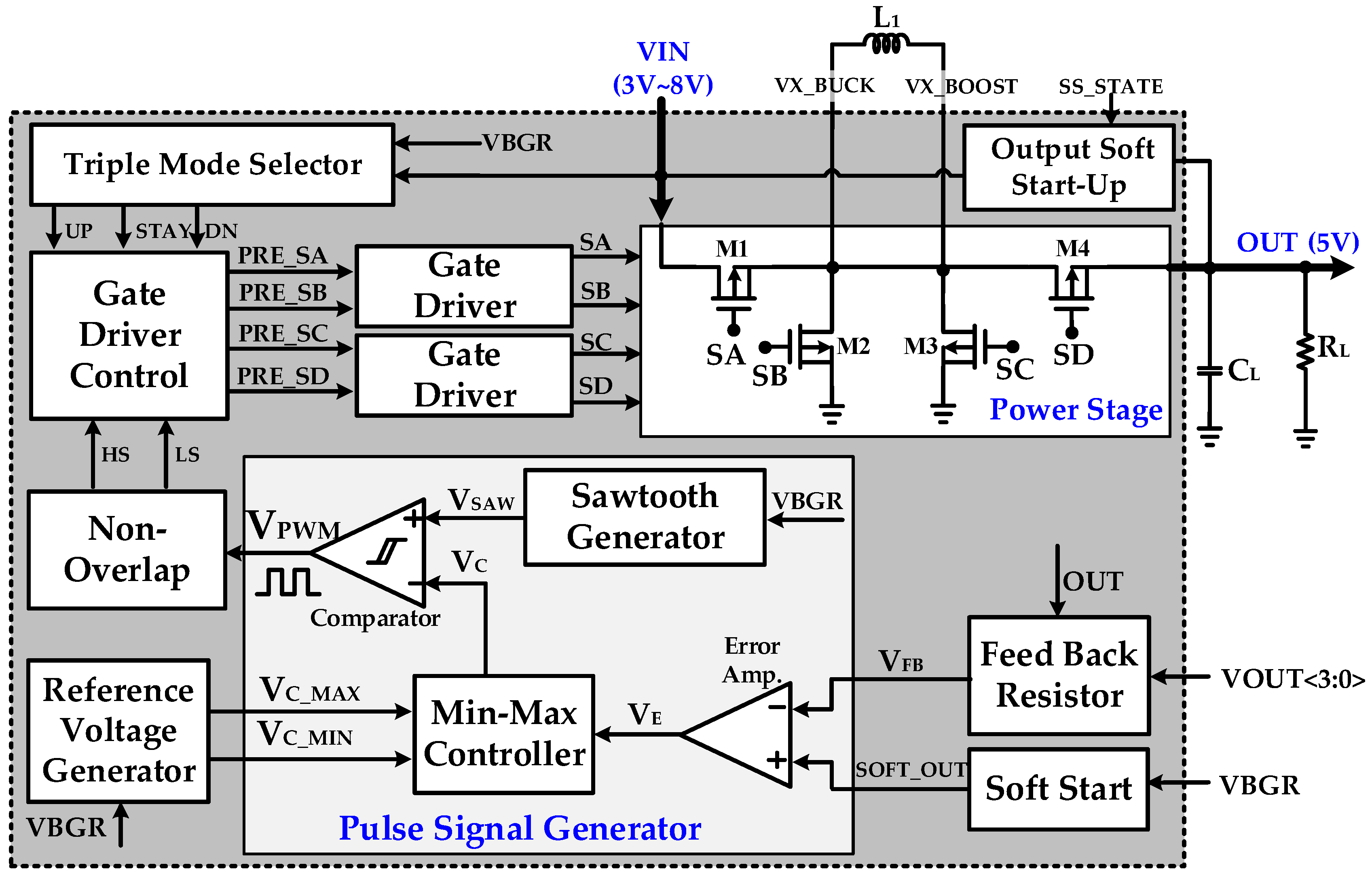
Figure 1 shows the overall structure of the proposed buck-boost DC–DC converter. The power stage of the proposed buck-boost DC–DC converter consists of four on-chip power switch transistors: M1, M2, M3, and M4. The switching activities of the four power transistors are controlled by signals SA, SB, SC and SD signal. In each mode of buck, boost, and buck-boost, the combinations of SA, SB, SC, and SD are different, and must be well controlled to obtain smooth transition between the modes. The operating modes of the proposed DC–DC converter are automatically decided based on the input voltage. When the input voltage is lower than 4.5 V, the converter operates in boost mode. When the input voltage is larger than 5.5 V, the converter operates in buck mode. When the input voltage is in between 4.5 and 5.5 V, the converter operates in buck-boost mode. Therefore, the control signals including SA, SB, SC, and SD are generated considering the input voltage VIN. The VOUT<3:0> are four output programmable trimming bits for adjusting the output voltage to obtain the accuracy voltage value.
2.1. Hysteresis Triple-Mode Selector and Gate Driver Controller
Three signals consisting of UP, DN, and STAY, are generated to determine the operating mode.
Figure 2 shows the logical dependency of the UP, DN, and STAY signals on the input voltage VIN. The UP, DN, and STAY signals are used to select the boost, buck, and buck-boost modes, respectively. When each signal is enabled, the DC–DC converter will operate in the corresponding mode. Therefore, the UP, DN, and STAY signals are enabled in different time windows, and there is no overlap presented in the enable state of the three signals during the operation of the DC–DC converter.
Practically, the change of the input voltage is due to the charge and discharge process of the battery. Therefore, the slope of the input voltage waveform is low, and fluctuating. The output voltage of the bandgap reference (BGR) also fluctuates, thus there will be an unstable state at the change between two modes. The unstable state of changing the mode may lead to high leakage current on the switch transistor that causes degraded efficiency or functional discontinuity that causes a poorly regulated output voltage.
To eliminate unstable mode transitions, hysteresis control technique is applied. A voltage gap of 50 mV is applied at the mode threshold voltage level of 4.5 and 5.5 V, as shown in
Figure 2. The input voltage VIN needs to cross over VL_HYS to make the DC–DC converter change the operating mode from boost to buck-boost. The input voltage needs to cross under VL, which is lower than VL_HYS by 50 mV, to make the DC–DC transfer from the current buck-boost mode back to the boost mode. A similar operation is applied when the DC–DC converter changes between buck-boost and buck mode. The hysteresis technique can totally remove the unstable mode control.
Figure 3 shows the circuit that performs the hysteresis control of the UP, DN, and STAY signals.
The UP, DN, and STAY signals control the distribution of the gate control signals including HS and LS to SA, SB, SC, and SD to turn ON/OFF the four power switching transistors M1, M2, M3 and M4, respectively.
Figure 2 shows the dependence of the SA, SB, SC, and SD signals on the UP, DN, and STAY signals. From this logical dependence, the circuit shown in
Figure 4 is implemented to perform the PWM distribution to realize the mode of power conversion. In
Figure 4, TIEH is tied to high logic value and TIEL is tied to low logic value.
Figure 5 shows the switching activities of the proposal in detail. In buck mode, M3 is always OFF, M4 is always ON, and M1 and M2 are controlled by SA and SB, which are HS and LS, respectively, to form the buck converter current flow. In boost mode, M2 is always OFF, M1 is always ON, and M3 and M4 are controlled by SC and SD, which are HS and LS, respectively, to form the boost converter current flow. In buck-boost mode, HS propagates to SA and SC, and LS propagates to SB and SD. The two pairs of transistors M1–M3 and M2–M4 are alternately ON and OFF to regulate the output to 5 V, while input voltage ranges 4.5–5.5 V.
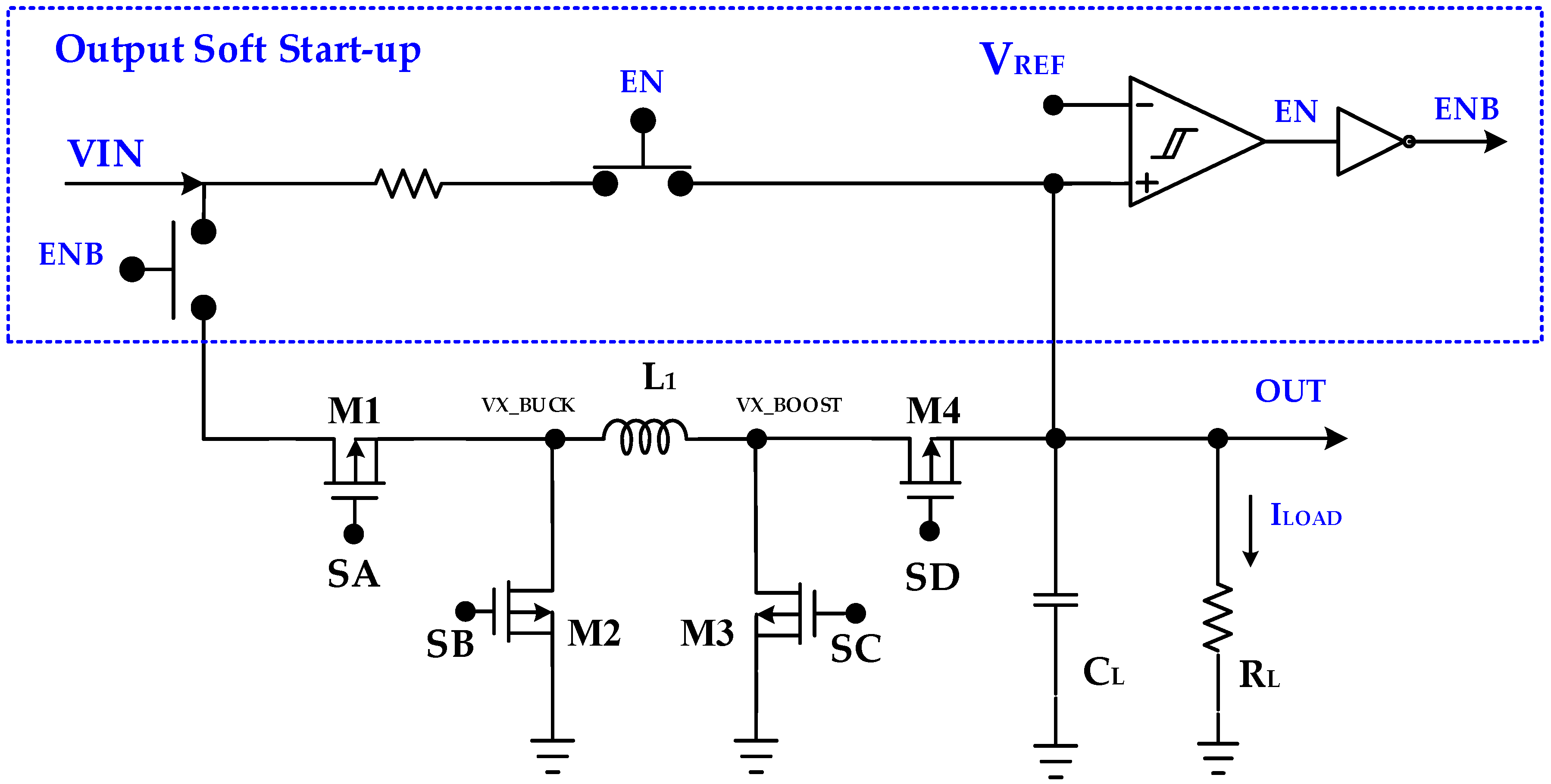
2.2. Output Soft Start-Up Circuit
When the DC–DC converter starts operating, a spike of current is drawn that is termed the inrush current. The inrush current generates conducted and radiated electromagnetic interference in the system [
21]. It triggers the upstream circuit breaker of the over-current protection of the system IC, and is usually higher than the load current of the DC–DC converter. Thus, the inrush current can drain out the battery energy or the storage power of the rectifier output capacitor, and reduce the efficiency of the DC–DC converter. In the RF energy harvesting system, the energy collected by the antenna is very low, due to the RF environment, antenna sensitivity and gain, impedance mismatch, and loss in the transmission line. The inrush current is significantly high, and takes a large portion of the harvested RF power. This inrush current significantly reduces the total efficiency of the RF energy harvesting system. In this circuit, a wide range of the input voltages are applied to the switch, and the voltage gap between the two terminals of the switch is unpredictable. The technique that is applied to reduce the inrush current must be simple, and adaptable to a wide range of input voltages.
In our design, to reduce the inrush current, we reduce the voltage gap between the source and the drain of the switch using the output soft start-up circuit. Initially, the output is charged up to 25% of the desired voltage level via a resistor, before the DC–DC converter enters the normal switching operation. Reducing the drain-source voltage of the switch reduces the inrush current. This technique affects the entire voltage range of the input supply.
Figure 6 shows the implementation of the output soft start-up circuit. Pre-charging the output voltage to a certain value reduces the time required for the output to reach the desired value. Therefore, the output soft start-up circuit also contributes to reduce the settling time of the DC–DC converter.
2.3. Pulse Width Modulation (PWM) Signal Min-Max Duty Generator
During the settling time, the output is not regulated, and thus the feedback voltage is out of the expected range. The unwanted feedback voltage value may cause the DC component of the output (VE) of the error amplifier (EA) to be higher or lower than the peak-to-peak voltage of the saw-tooth signal (VSAW). When the DC component of VE is higher than the maximum peak of VSAW, the output of the pulse signal generator VPWM is maintained at zero or the pulse width of the VPWM signal, in this case, is 0% of the duty cycle. The output of the DC–DC converter will never be charged up. When the DC components of VE are lower than the minimum of VSAW, the pulse width of PWM is 100% of the duty cycle, and it causes the over-charging of the output voltage. This phenomenon extends the settling time of the DC–DC converter. To overcome this situation, the min-max duty generator block controls the DC component of the output of EA.
In our design, the V
SAW signal oscillates in the voltage range of 0–1.2 V. The DC component of the output of the error amplifier needs to be controlled over the range of V
C_MIN to V
C_MAX of 0.1–1.1 V for safe operation.
Figure 7 shows the min-max duty generator schematic. When the output of EA is lower than the V
C_MIN, the V
C_MIN value is selected to compare with V
SAW to create the PWM signal. In this case, the pulse width of the V
PWM is maximized at 91.7%. When the output of the EA rises higher than V
C_MAX, the V
C_MAX voltage controls the comparator generating the output PWM at the minimum pulse width of 8.3% of the duty cycle. Otherwise, the V
E is directly compared with the V
SAW to generate the V
PWM.
3. Experimental Results
Figure 8 shows the microchip photograph of the proposed buck-boost DC–DC converter. The proposed DC–DC converter is implemented using the 180 nm CMOS process. The total area including PADs is 1.55 mm × 1.14 mm. Just 50% of the chip is occupied by the power-switching transistor.
Figure 9 shows the top simulation results of the proposed buck-boost DC–DC converter. In this simulation, the input voltage VIN is swept from 2 to 8 V, the signal UP/STAY/DN goes high one-by-one, and the buck-boost DC–DC converter operates in boost, buck-boost, and buck mode, respectively. When the input voltage reaches 3 V, the UP signal starts to go high, and the DC–DC converter enters the boost mode. After the settling time, the output voltage is regulated, and stable at 5.06 V.
When the input voltage VIN is in the range 4.5 to 5.5 V, the UP signal turns low, and the STAY signal goes high at the same time, to let the DC–DC converter operate in the buck-boost mode. Similarly, when the input voltage goes higher than 5.5 V, the STAY signal is low, the DN signal turns high, and the DC–DC converter enters the buck mode. The output voltage OUT of the proposed buck-boost DC–DC converter is regulated to about 5 V in the three modes. During the mode transition, the output voltage has a voltage undershoot of 60 mV. This undershoot voltage can be eliminated by using the trimming bits VOUT<3:0> to get stable output voltage.
After the chip tape-out, we conducted packaging and test setup to measure the proposed DC–DC converter.
Figure 10 shows the measurement set-up environment, which consists of the test board, Serial Peripheral Interface (SPI) board, SPI control, power supplies, electronic load, and oscilloscope. The purpose of the SPI board is to provide the enable bit control and trimming bit.
Figure 11a–c show the measurement results of the proposed buck-boost DC–DC converter in boost, buck-boost, and buck modes, respectively, when the input voltage are 4.47, 5.15, and 7.08 V. The output voltage in three modes is regulated to 5.06, 5.02, and 5.09 V, respectively. The switching frequency shown in the measured waveform is well matched to the simulation result, which is around 3.2 MHz. The switching frequency is well maintained over the three operations of boost, buck–boost, and buck mode at 3.22, 3.24, and 3.24 MHz, respectively.
The measurement results in
Figure 11a–c are obtained with the load condition of 100 mA. The input voltage of 5.5 V maximizes the gap between the line regulation simulation and measurement results. This is due to the undershoot voltage of the transition point. The real delay of the buck-boost to buck mode changing time is slightly higher in the real circuit, which causes larger undershoot voltage.
Figure 11d shows the line regulation performance of the proposed buck-boost DC–DC converter over the input voltage range of 3–8 V. In the simulation, the line regulations at the load currents of 100 mA and 500 mA are consistent. The variation of the output voltage over the input range of 3–8 V is 60 mV, which is roughly less than 1.2% of the output voltage. Although the measured line regulation of the proposed DC–DC converter is slightly different from the simulation results, the overall trend is similar. The maximum deviation between the simulation and the measurement results, at the load current of 100 mA is only 0.79%. The maximum deviation between the simulation and the measurement results, at the load current of 500 mA is 1%. Both of the maximum deviations in the two measurements occur at the input voltage of 5.5 V. These differences are due to the measurement parasitics and measurement error.
To show the wide input range regulation ability of our proposed buck-boost DC–DC converter, we measured the output voltage of our converter with the input voltage range of 3–8 V at 1 V step. The measurement results are shown in
Figure 12. The load current used in this measurement is similar to the previous results in
Figure 11 that is 100 mA. We can see a smooth regulation of the output according to the input voltage. A slightly change at the point of input voltage jumping between 3 V and 4 V, but this change is within the acceptable regulation range.
The power conversion efficiency of our proposed converter is measured and plotted in
Figure 13. The load conditions of 100 mA and 500 mA are used while measuring the power conversion efficiency (PCE). The efficiency is maintained relatively high over the wide range of the input voltage with both load current condition.
The performance of the proposed buck-boost DC–DC converter is compared with previous works to show the advantages of this proposal. The proposed converter can maintain a constant output voltage over the widest range of input voltages, in comparison to the previous works. Our proposed buck-boost converter operates over three mode buck, buck-boost, and boost mode for better output regulation. In terms of voltage conversion efficiency, the proposed DC–DC converter also has high efficiency of 94.8%, compared to the 91%, 91%, 93.5%, 89.3%, and 85.5% of the work in [
14,
15,
16,
17], respectively. In term of maximum load current, our DC–DC converter provides a reasonable output current at 500 mA for mid-range power application.
Table 1 shows that the proposed converter has a reasonable maximum load current, die area, and the inductor/capacitor size, compared to the related works.

 ,
, 


