Article

General Analysis of Switching Modes in a Dual Active Bridge with Triple Phase Shift Modulation

1
Power Electronics System Group, Universidad Carlos III de Madrid, 28911 Leganes, Spain
2
Centre of Industrial Electronics, Universidad Politecnica de Madrid, 28001 Madrid, Spain
*
Author to whom correspondence should be addressed.
Energies 2018, 11(9), 2419; https://doi.org/10.3390/en11092419
Submission received: 11 August 2018 / Revised: 6 September 2018 / Accepted: 7 September 2018 / Published: 12 September 2018
(This article belongs to the Section F: Electrical Engineering)

Abstract

:
This paper provides an exhaustive analysis of the Dual-Active-Bridge with Triple-Phase-Shift (DAB-TPS) modulation and other simpler ones, identifying all the possible switching modes to operate the DAB in both power flow directions, and for any input-to-output voltage range and output power. This study shows four cases and seven switching modes for each case when the energy flows in one direction. That means that the DAB operates up to fifty-six different switching modes when the energy flows in both directions. Analytical expressions for the inductor current, the output power, and the boundaries between switching modes are provided for all cases. Additionally, the combination of control variables to achieve Zero-Voltage-Switching (ZVS) or Zero-Current-Switching (ZCS) is provided for each case and switching mode, by showing which switching modes obtain ZVS or ZCS for the whole power range and all switches—independent of the input-to-output voltage ratio. Therefore, the most interesting cases, switching mode and modulation for using the DAB are identified. Additionally, experimental validation has been carried out with a 250 W prototype. This analysis is a proper tool to design the DAB in the optimum switching mode, reducing the RMS current and achieving to increase efficiency and the power density.

1. Introduction

Currently, the Dual-Active-Bridge (DAB) converter is commonly found in different sectors such as in electric vehicles, in which DAB converters are used as battery charges [1,2] or as active balancing systems [3]. The aeronautics industry is betting on improving emissions and reducing fuel consumption by replacing mechanical and pneumatic systems with electrical systems. In Reference [4] is shown a DAB working in harsh environments with high temperature as a component of an electric actuator; Reference [5] shows a DAB as an interface between the battery storage system and DC bus. Additionally, for electric ships [6,7] and smart grids [8,9,10], DAB converters can be seen as an interface component in the medium-voltage grid. DAB converters are also an alternative for electrochemical energy storage as shown in References [11,12].
The conventional DAB topology consists of two active bridges, a high-frequency transformer (T) and a series inductor (L)—Figure 1. The main characteristics of the DAB are bi-directionality, galvanic isolation, high power density, and soft switching in some operating conditions. Additionally, in the state-of-art, a variant of the DAB without transformer can be found, for application in mobile phones and computer chargers [13].
The most basic modulation applied to DAB is the Phase-Shift (PS), also known as Single-Phase-Shift (SPS), where simplicity its main advantage. In this case, it is only necessary to control the phase shift (φ) between the output voltage (v11 and v22) of the bridges, with D1 = 1 (pulse width of voltage v11) and D2 = 1 (pulse width of voltage v22)—Figure 2a. However, this kind of modulation has some disadvantages such as reduction of the operating range with Zero-Voltage-Switching (ZVS) or Zero-Current-Switching (ZCS), if the input-to-output voltage ratio moves away from the unity, and high currents at low power. Therefore, PS is not a proper modulation for wide output and input voltage ranges in the converter [14].
Another modulation scheme applied in DAB is the Extended-Phase-Shift modulation (EPS). This modulation operates by using the Phase-Shift (φ) between output voltages of the bridges, as in the PS modulation, along with the pulse width variation of the Bridge 1 output voltage (D1), being D2 = 1, Figure 2b. EPS modulation reduces the circulating energy and the conduction losses for medium power, therefore improving the performance compared to the PS modulation [15,16,17,18,19], although with a reduced impact for low power.
Additionally, with two degrees of freedom, the Dual-Phase-Shift modulation is well known (DPS) [20]. This modulation uses, once more, the Phase-Shift (φ) between output voltages of the bridges, as in the EPS modulation, along with the pulse width variation of both Bridges output voltages (D1, D2), in this case being D1 = D2, Figure 2c.
A more enhanced alternative is Triple-Phase-Shift modulation (TPS), which involves three control variables: The pulse width of the output voltages of Bridge 1 (D1) and Bridge 2 (D2), and the phase shift (φ) between both voltage waveforms, Figure 2d. This modulation strategy improves the converter’s performances, with a more significant impact at low power, reduces RMS current, and presents a higher probability of soft switching operation [21,22,23]. However, the complexity increases due to the higher number of parameters to be controlled, which results in a higher number of possible switching modes of the converter [24,25,26,27,28]. There are different combinations of the three control variables that satisfy the same requirements of transferred power between the input and output ports of the converter. However, not all the combinations imply the same performance from switching conditions and circulating currents.
Many works can be found in the state-of-the-art that are focused on the study of the DAB switching modes, ZVS and ZCS operation, or RMS current reduction, among other topics. In References [26,27], the authors identify five switching modes (considering positives mismatches); in Reference [28], the number of switching modes increases to twelve (considering positive and negative mismatches), all of them for condition V1 > n·V2. In Reference [29], the authors analyse the charge and discharge of the parasitic MOSFET capacitances to get ZVS. On the other hand, Reference [30] analyses the reduction of the transformer's coupling to achieve the same effect. However, all these works show useful partial solutions, but without doing a general analysis of all operation possibilities.
Therefore, the contribution of this paper is oriented to provide an exhaustive analysis of the different DAB switching modes when TPS, EPS, and PS modulation (DPS can be considered a particular case of TPS) are applied to get the best performance for whole output power range, and considering each V1 and V2 ratio (that includes buck and boost modes). Thanks to this in-depth analysis, the best switching modes are identified as well as the most combinations of the modulation variables to guarantee Zero-Voltage-Switching (ZVS) or Zero-Current-Switching (ZCS). This analysis is a tool to design the DAB converter, ensuring the soft-switching operation, and to improve the efficiency and the power density.
This paper organises as follows: Section 2 presents the basic operation of the TPS modulation applied to the DAB. Section 3 defines the Cases of study (based on bridges output voltages and their duty cycles) and the switching modes when TPS modulation is used, along with the inductor current expressions and the transmitted power for each switching mode. Section 4 analyses and calculates the expressions to get soft switching in the converter for each Case and switching mode. Section 5 validates the analysis for Case I and Case II with a 250 W prototype developed in the laboratory. Finally, Section 6 summarises the conclusions of the work carried out.

2. Triple-Phase-Shift Modulation

Triple-Phase-Shift (TPS) consists of shifting the driving signals vg3, vg5 and vg7 with respect to vg1 (corresponding to the switches M3, M5, M7, and M1, respectively). By driving the switches in this way, v11 is generated at the output of the Bridge 1 of amplitude V1, v22 is generated in the primary side of the transformer with an amplitude of V2/n, and a current iL flows through the inductor L.
Three control parameters define TPS modulation: D1 (0 < D1 ≤ 1) representing the pulse width of voltage v11, D2 (0 < D2 ≤ 1) representing the pulse width of v22 and φ (−π < φ < π) measures the phase shift between v11 and v22, as shown in Figure 3.
The switching instants of the voltages v11 (t1LH and t1HL) and v22 (t2LH and t2HL), shown in Figure 3, are calculated by Equation (1), considering that the positive part of v11 centres in Tsw/4.
t 1 LH = T sw 2 · ( 1 2 D 1 2 ) t 1 HL = T sw 2 · ( 1 2 + D 1 2 ) t 2 LH = T sw 2 · ( φ π + 1 D 2 2 ) t 2 HL = T sw 2 · ( φ π + 1 + D 2 2 )

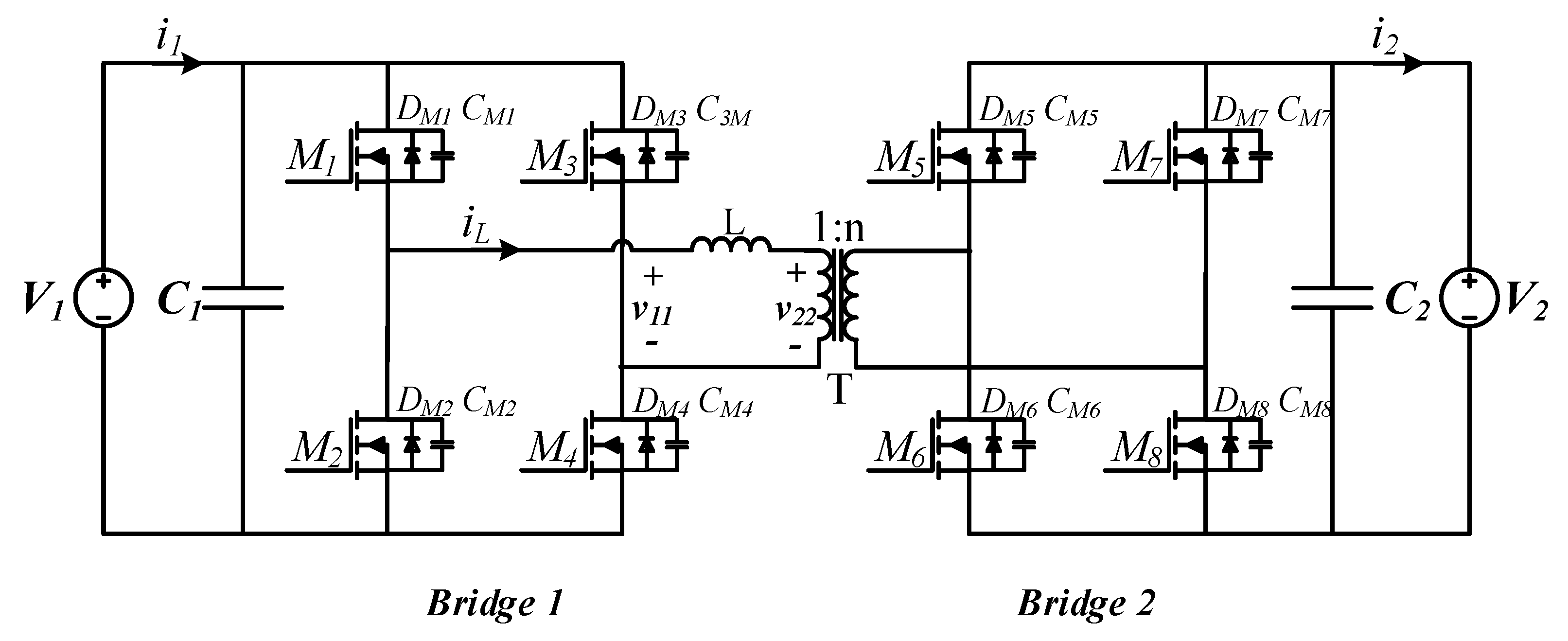
3. Cases and Switching Modes

The switching modes define according to the profile acquired by the current iL in each operating state. The current iL is defined by the input parameters of the converter (V1, V2, n, L, fsw) and by the parameters of the TPS modulation (D1, D2 and φ). By considering n, L and fsw as constants, the voltages v11, v22 and the pulse widths D1 and D2, four cases of study can be defined:
Case I: v11 ≥ v22 and D1 > D2
Case II: v11 ≥ v22 and D1 ≤ D2
Case III: v11 < v22 and D1 > D2
Case VI: v11 < v22 and D1 ≤ D2.
In Reference [20], the author concluded that the analysis performed for positive φ is equivalent to negative φ; therefore, DAB can operate in eight cases of study. Additionally, for positive φ, it can be observed that there are equivalences between Case I and Case IV, as well as between Case II and Case III; they obtain by exchanging v11 with v22, and D1 with D2. It means that only the analysis of two of them is necessary. Therefore, in this paper, the analysis is developed for the Case I and II.

3.1. Switching Modes: Case I and Case II. Boundaries

The total switching modes per Case are seven: SM1, SM2, SM2*, SM3, SM3*, SM4, and SM5; they can have positive or negative φ angle values (bidirectionality). Therefore, considering bi-directionality, four cases and seven switching modes per case, DAB can operate up to fifty-six switching modes. As aforementioned, Cases I and II are only analysed for positive φ angle values, as shown in Figure 4 and Figure 5, respectively. These switching modes are obtained by increasing the phase shift φ for any value of D1 and D2.
The boundaries in each switching mode are obtained when the switching instants of the voltages v11 and v22 occur at the same time. For example, for SM2 in Figure 4b: t1HL = t2HL determines the lower boundary (switching mode from SM1 to SM2,) and the upper one when t1HL = t2LH (switching mode from SM2 to SM3,), as shown in Equation (2).
Lower   boundary :   ( D 1 D 2 2 ) · π Upper   boundary : ( 1 D 1 + D 2 2 ) · π
The switching modes SM2 and SM3 are obtained for D1 < 1 − D2, whereas SM2* and SM3* are obtained for D1 ≥ 1 − D2. The switching mode SM2* is different concerning SM2 only in the boundaries, whereas SM3* is different regarding SM3 in the boundaries, the current profile and the expression of the power, with respect to those in SM3. Table 1 summarises the boundaries of all switching modes for Case I and Case II.
From the information in Table 1, the switching modes are plotted in a three-dimensional way depending on the parameters D1, D2 and φ, forming a cube with the unity side, as shown in Figure 6. The tetrahedral volumes contain the switching modes obtained with TPS modulation. In Case I: the modes SM2 (DEFG), SM2* (CEFG), SM3* (BCEG) and SM4 (ABEG), are shown in Figure 6a; and the modes SM1 (CDEI), SM3 (ADEG), and SM5 (ABEH) are shown in Figure 6b. For Case II: the modes SM2 (DFGJ), SM2* (CFGJ), SM3* (BCGJ), and SM4 (ABGJ) are shown in Figure 6c; while, the modes SM1 (CDJL), SM3 (ADGJ), and SM5 (ABJK), are shown in Figure 6d.

3.2. Current Through the Inductor L

The current iL in each switching mode is calculated from Figure 4 (Case I) and Figure 5 (Case II), together with Equation (3) for four consecutive switching instants.
v L = L di L dt
As an example, Figure 5a has t2LH, t1LH, t1HL and t2HL as consecutive switching instants and iL(t) = −iL(t + Tsw/2); therefore, iL(t) must be calculated for half the switching period. Equation (4) shows iL(t) from t2LH to t2HL by applying Equation (3) and the equation systems in Equation (5) are obtained when switching instants are replaced in iL(t). Table 2, at Case II (column) and SM1 (row), shows the solution of Equation (5).
i L ( t ) = { i L ( t 2 LH ) 1 L · V 2 n · ( t t 2 LH ) ;   t 2 LH t < t 1 LH i L ( t 1 LH ) + 1 L · ( V 1 V 2 n ) · ( t t 1 LH ) ;   t 1 LH t < t 1 HL i L ( t 1 HL ) 1 L · V 2 n · ( t t 1 HL ) ;   t 1 HL t < t 2 HL
i L ( t 1 LH ) = i L ( t 2 LH ) 1 L · V 2 n · ( t t 2 LH ) i L ( t 1 HL ) = i L ( t 1 LH ) + 1 L · ( V 1 V 2 n ) · ( t t 1 LH ) i L ( t 1 HL ) = i L ( t 1 HL ) 1 L · V 2 n · ( t t 1 HL ) i L ( t 2 HL ) = i L ( t 2 LH )
Using the same procedure for each switching mode, Table 2 gathers the current iL at the switching instant for Case I and Case II.

3.3. Average Power

The input current, i1(t), is defined from t1LH to t1HL when the power is flowing to V2. Without considering losses, the average power (P = V1·I1) is calculated by Equation (6) and iL at the switching instant (Table 2). This average power is detailed for each switching mode in Table 2.
P = V 1 · 2 T sw   t 1 LH t 1 HL i L ( t ) dt

4. Soft Switching

In general, soft switching is obtained either by Zero-Voltage-Switching (ZVS) or by Zero-Current-Switching (ZCS) of the converter switches. ZVS is achieved by switching on the switches M1, M4, M6 and M7 when iL < 0, and in the switches M2, M3, M5 and M8 when iL > 0. ZCS is achieved in all switches when iL = 0, during switching-off. Table 3 describes, in detail, the soft switching conditions as a function of the current iL(t) for each switch in the converter.
For the sake of simplicity, the analysis described in this section is made without taking into account the parasitic inductances, capacitances, and resistances that are in real converters. In particular, MOSFET’s parasitic capacitances that affect the soft switching conditions. The capacitances effect on the DAB has been previously analysed in several papers [26,31,32,33].

4.1. Case I (v11 ≥ v22 and D1 > D2)

Table 4 is obtained by combining the current iL(t) through the inductor shown in Table 2 and the information in Table 3. Table 4 collects all the specific conditions to obtain ZVS or ZCS for all the switches in each switching mode for the Case I. ZCS is achieved when the equations are satisfied; ZVS is achieved when the inequalities are satisfied, for example: M1 has ZVS when (D1·V1·n > D2·V2) and ZCS (D1·V1·n = D2·V2) for SM1. Additionally, those conditions are classified into two types: depending on φ and non-depending on φ.

4.1.1. Non-Depending on φ

The non-depending on φ conditions (Table 4) summarise in the three expressions shown in Equation (7). The first condition (D1·V1·n ≥ D2·V2) only fulfils when D1·V1·n > D2·V2 due to the Case I implies v11 ≥ v22 and D1 > D2. It means that switches with this condition have ZVS. However, the second condition (D1·V1·n ≤ D2·V2) cannot be satisfied. Therefore, the switches depending on this condition switch with losses (Hard Switching). Finally, the last condition (D1·V1·n + D2·V2 ≥ 0) can be satisfied for all the possible values of D1, D2 and n.
D 1 V 1 · n V 2 D 2 D 1 V 1 n V 2 D 2 D 1 V 1 n + V 2 D 2 0

4.1.2. Depending on φ

The conditions that depend on φ must be graphically analysed in a cube with the unity side. The switching mode SM3* for the Case I is analysed, by considering the voltage ratio shown in Equation (8), to illustrate the procedure.
d = V 2 n · V 1
Equation in (9) show soft switching conditions from Table 4 by considering Equation (8). The plane SSij (D1, D2) represents the soft switching conditions for “i” and “j” switches with any D1 and D2. Figure 6a and soft switching conditions in Equation (9) are plotted in Figure 7a for SM3*. In Figure 7a, the switching mode SM3* is represented by tetrahedron BCEG, and SS12 (D1), SS34 (D1), SS56 (D2) and SS78 (D2) are represented by the planes AKWX, DLYZ, DIUT, and AHTU, respectively.
Figure 7b–e show the projections of the soft switching conditions and SM3* region onto the planes φ/π − D1 and φ/π − D2.
SS 12   ( D 1 , d ) = φ π = [ 1 D 1 2 · ( 1 + 1 d ) ]     D 2 SS 34   ( D 1 , d ) = φ π = [ D 1 2 · ( 1 1 d ) ]     D 2 SS 56   ( D 2 , d ) = φ π = [ D 2 2 · ( 1 d ) ]     D 1 SS 78   ( D 2 , d ) = φ π = [ 1 D 2 2 · ( 1 + d ) ]     D 1
Figure 7b shows that M1 and M2 have soft switching for angles φ/π ≥ SS12 (D1,d). It has been indicated by the region in which φ/π ≥ SS12 (D1,d) (in grey), and the values D1 and φ belonging to switching mode SM3* (in green). All combination D1 − φ/π, belonging to SM3*, fulfil with φ/π ≥ SS12 (D1,d), which means that both switches (M1 and M2) have soft switching for the entire operating range of SM3*. The condition that allows having soft switching in the switches M3 and M4 fulfils if φ/π ≥ SS34 (D1,d), Figure 7c. The condition SS34 (D1,d) takes negative values for the range 0 < D1 < 1, this means that M3 and M4 always switch to soft switching for φ/π > 0.
Figure 7d shows that the projection of the tetrahedron belonging to SM3* onto the φ/π − D2 axes is the BCE plane. For the angles φ/π = SS56 (D2,d) and φ contained in the BCE triangle, ZCS is achieved in M5 and M6; on the other hand, when φ/π > SS56 (D2,d) and the BCE triangle contains to φ/π, M5 and M6 have ZVS. Similarly, switches M5 and M6, M7 and M8 have ZCS when φ/π = SS78 (D2,d) and ZVS for φ/π > SS78 (D2,d), and the BCE triangle contains to φ/π, Figure 7e. Finally, Figure 7f shows the values for D1, D2 and φ/π, in pink, that allow all the switches to have soft switching for SM3*. From Figure 7f, it can be concluded that ZCS is only possible for switches M7 and M8 when the plane GTV contains to D1, D2 and φ/π; for the rest of the points belonging GBVT volume, all the switches have ZVS.
Table 5 summarises the type of turn on each switch for all switching modes, and the condition to get soft switching on the Bridge 2 switches.
Figure 8 shows the switching modes, power flow, RMS current through the inductor, and the boundary between HS and ZVS for M5 to M8 (conditions in Table 5) when D1 takes different values (0.3, 0.6 and 0.95). Figure 8a,b depict the power flow and the RMS current for D1 = 0.3 (D1 ≤ 0.5), and the switching modes SM1, SM2, SM3, SM4, and SM5. For D1 = 0.6 (D1 > 0.5), two new switching modes appear, SM2* and SM3*, in the power flow, Figure 8c, and RMS current, Figure 8d. Finally, when D1 = 0.95 both power flow, Figure 8e, and inductor RMS current, Figure 8f, tend to achieve the maximum levels. In short, higher power is obtained when D1 is close to 1. For the same power flow, switching modes SM1, SM2, SM2*, and SM3* have less inductor RMS current than the rest of them, see Figure 8b,d,f. Soft switching in all switches, Table 5, is possible in SM4, SM5, and SM3*, but SM3* obtains the lowest inductor RMS current when D1 > 0.5, Figure 8d,f. When D1 ≤ 0.5 less RMS currents appear in SM1 and SM2, see Figure 8b, but all switches in bridge 2 are in hard switching, see Table 5.

4.2. Case II (v11 ≥ v22 and D1 ≤ D2)

Similar to Case I, Table 6 summarises the conditions that allow the converter to have soft switching on all switches, considering positive φ. This table is equivalent to Table 4 for Case I. Again, there are two types of conditions that have soft switching: Those depending and those non-depending on φ.

4.2.1. Non-Depending on φ

As in Case I, the non-depending on φ conditions are shown in Equation (7), and all conditions could be fulfilled due to V1·n ≥ V2 and D1 ≤ D2, for Case II. So, from the first and the second conditions (D1·V1·n ≥ D2·V2 and D1·V1·n ≤ D2·V2) is obtained in Equation (10) as the only solution that meets both conditions at the same time, which means that the switches have ZCS. The third condition (D1·V1·n + D2·V2 ≥ 0) always fulfils because all its parameters are always positive, which means that the corresponding switches achieve ZVS.
D 1 · V 1 · n = D 2 · V 2
The switching modes depicted in Figure 6c,d, for Case II, are simplified in Figure 9a when expression in Equation (10) is applied, turning the original volumes into planes. On the other hand, the application of the expression in Equation (10) implies a limitation to reach the maximum power in the converter due to the maximum value for D1 = d, which is got when D2 = 1. In order to reach the maximum power, the expression in Equation (10) has not been considered for d < D1 < 1 and remaining as a constant D2 = 1, as shown in Figure 9b. Note that the condition of this last interval coincides with the EPS modulation.

4.2.2. Depending on φ

Applying the expression in Equation (10), in Table 6, for 0 < D1 ≤ d, the four conditions shown in Equation (11) summarise those that depend on φ.
φ ( D 2 D 1 2 ) · π φ ( D 2 D 1 2 ) · π φ ( 1 D 2 + D 1 2 ) · π φ ( 1 + D 2 + D 1 2 ) · π φ ( D 2 D 1 2 ) · π
The first condition (φ ≥ − (D2 − D1)·π/2) indicates that the switches achieve soft switching when φ ≥ − (D2 − D1)·π /2. In Case II it is only possible to obtain ZVS for φ > 0 due to D1 ≤ D2. The second condition means that ZVS is achieved when 0< φ < (D2 − D1)·π/2, ZCS for φ = (D2 − D1)·π/2 and HS in any other case. The third condition (φ ≥ (1 − (D2 + D1)/2)·π) indicates ZVS for φ > (1 − (D2 + D1)/2)·π), ZCS for φ = (1 − (D2 + D1)/2)·π) and HS for φ < (1 − (D2 + D1)/2)·π). The fourth condition (φ ≤ (1 − (D2 + D1)/2)·π) indicates ZVS for φ < π, since for φ = π the output power is equal to zero. Finally, the fifth condition means that ZVS is achieved when φ > (D2 − D1)·π/2, and ZCS for φ = (D2 − D1)·π/2 and HS in any other case.
Therefore, by fulfilling expression in Equation (10), φ > 0 from first condition (lower boundary for SM1, Table 1, Case II), up to φ ≤ (D2 − D1)·π/2 from the second condition (upper boundary for SM1, Table 1, Case II), all switches for SM1 get soft switching, see Table 6. By fulfilling expression in Equation (10) and φ ≥ (D2 − D1)·π/2 from the fifth condition (lower boundary for SM2 and SM2*, Table 1, Case II), all switches for SM2 and SM2* get soft switching. Only by fulfilling expression in Equation (10) do all switches for SM3 get soft switching, see Table 6. In addition, by fulfilling expression in Equation (10) and φ ≥ (1 − (D2 + D1)/2)·π from the third condition (lower boundary for SM3*, Table 1, Case II), all switches for SM3* get soft switching, see Table 6. By fulfilling expression in Equation (10) and φ ≥ (1 − (D2 + D1)/2)·π from the third condition (lower boundary for SM4, Table 1, Case II), all switches for SM4 get soft switching. Finally, by fulfilling expression in Equation (10), φ ≥ (1 − (D2 + D1)/2)·π from the third condition (φ values less than the lower boundary for SM5, Table 1, Case II), and φ < 1 from the fourth condition, all switches for SM5 get soft switching.
That means, for the simple fact of working in each switching mode, it would be fulfilling these conditions and having soft switching.

4.2.3. Extended Switching Modes

As said above, when analysing the non-depending on φ conditions, to overcome the limitation on the power delivered due to the early saturation of D2, an additional condition that coincides with EPS modulation have to be considered. This operating zone is going to be called Extended Switching Mode, Figure 9b. The soft switching conditions in the Extended Switching Mode (D1 > d and D2 = 1) are shown in Table 6, for the switching modes SM1, SM3* and SM5. The boundaries of these three switching modes for the Extended Switching Mode are included in Table 7 and are shown in Figure 10a.
Additionally, soft switching conditions for the Extended Switching Mode are divided into those depending on φ and those non-depending on φ.
From Table 6 and D2 = 1, the conditions that do not depend on φ are summarised in two equations, as shown in Equation (12). The first condition (D1 ≤ d) affects to SM1, meaning that the switches M5–M8 for D1 > d lose the soft switching, see Figure 10b. The second condition (D1·V1·n + D2 ≥ 0) is always fulfilling, and only affects SM5, which implies ZVS in switches M5–M8, see Figure 10b.
D 1 d D 1 · V 1 · n + D 2 0
On the other hand, the depending on φ conditions for the same three switching modes (SM1, SM3* and SM5), Table 6, are analysed similarly for D1 < d. From Table 6 and considering Equation (8), for Case II d ≤ 1 (v22/v11 = V2/(n·V1) = d ≤ 1). For SM1, the first condition (φ ≤ (−D1/2·(1 − 1/d))·π or φ ≤ (D1/2·((1/d) − 1))·π) allows soft switching in M1–M2, line blue in Figure 10a, and the second condition (φ ≥ D1/2·(1 − 1/d)·π) is equivalent to consider φ > 0 due to d ≤ 1, this means M3–M4 always have soft switching, see Figure 9a.
Soft switching conditions for SM3* can be simplified as (φ ≥ (1 − D1·(1 + 1/d)/2)·π), (φ ≥ (D1·(1 − 1/d)·π/2)) and (φ ≥ (1 − d)·π/2), from Table 6; the third condition (φ ≥ (1 − D1·(1 + 1/d)/2)·π), red line in Figure 10a) indicates soft switching for M1–M2; the fourth condition (φ ≥ (D1·(1 − 1/d)/2)·π) is equivalent to φ > 0 due to d ≤ 1, this means M3–M4 always have soft switching; and the fifth condition (φ ≥ (1 − d)·π/2, horizontal black dashed line in Figure 10a means soft switching for M5–M8.
Finally, soft switching conditions for SM5 are (φ ≥ (1 − D1·(1 + 1/d)/2)·π) and (φ ≤ (1 + D1·(1 + 1/d)/2)·π); the sixth condition (φ ≥ (1 − D1·(1 + 1/d)/2)·π, red line, means soft switching for M1–M2, the seventh condition (φ ≤ (1 + D1·(1 + 1/d)/2)·π) is equivalent to φ < π and it indicates soft switching for M3–M4, see Figure 10a.
Depending and non-depending soft switching conditions are summarised in Table 8 and Figure 10b for D1 > d and D2 = 1. All the switches have zero voltage switching in the ZVS zone (blue dashed rectangle). For SM1, M1–M2 always have hard switching; and for SM3* and φ < (1 − d)·π/2, M5 to M8, always have hard switching, see HS zone (red dashed rectangle). Table 8 shows the results of the analysis performed for Case II and shows the ranges of each switching mode, the power transferred and the type of switching in the switches.
Figure 10c,d shows the power flow and the inductor RMS current, respectively. As depicted, the lower RMS current can be obtained at the boundary between SM1, SM2 and SM2*, compared with SM3, SM4 and SM5 for the same transferred power.

5. Experimental Results

This section shows the experimental results for Case I and Case II using a 250 W prototype. The prototype has IRFP4468PbF MOSFETs in both bridges, a transformer built with an ETD59 ferrite core and a self-manufactured inductor with a RM12 ferrite core. Additionally, a TMS320F28335 Texas Instrument DSP generates the driving signals.
Table 9 summarises the operating parameters of the converter, and Figure 11 shows a block diagram of the experimental circuit layout.
Figure 12 shows six switching modes (SM1, SM2, SM2*, SM3*, SM4, y SM5) for Case I and d = 0.677, which validate the analysis performed about the switching types, detailed in Table 5. Figure 12a–c show ZVS in M1, M2, M3, and M4; HS in M7 and M8; and for M5 and M6 the switching type depend on φ and D2. In Figure 12d–f, the switching type for M7 and M8 varies in function of φ and D2, whereas the rest of switches maintain the same switching type (ZVS). Figure 12a shows the voltages v11, v22 and iL for the switching mode SM1, in which the four switches of the Bridge 1 (M1–M4) are operating with ZVS. On Bridge 2, switches M5 and M6 switch with losses (HS) due to (φ/π = 0.050) < (SS56 = 0.059), as shown in Table 5, for D1 = 0.5 and D2 = 0.34. Switches M7 and M8 are in HS, as was specified in Table 5. In Figure 12b, the eight switches switch in the same way as shown in Figure 12a, for D1 = 0.5, D2 = 0.45 and (φ/π = 0.061) < (SS56 = 0.075). In the switching mode SM2*, Figure 12c shows ZVS in M5 and M6 for (φ/π = 0.222) > (SS56 = 0.077) with D1 = 0.75 and D2 = 0.487. Figure 12d shows the switching mode SM3* with ZVS in M7 and M8 when D1 = 0.75, D2 = 0.643 and (φ/π = 0.577·π) > (SS78 = 0.494). In Figure 12e, switches M7 and M8 achieve ZVS for D1 = 0.75, D2 = 0.5 and (φ/π = 0.722) > (SS78 = 0.667) in the switching mode SM4. For the last switching mode, SM5, the parameters D1 = 0.75, D2 = 0.2, and (φ/π = 0.75) < (SS78 = 0.833) are considered as having HS in M7 and M8, as predicted in Table 5, Figure 12f.
Figure 13 shows six switching modes (SM1, SM2, SM3, SM4, SM5, and SM3*) for Case II and d = 0.677, applying Equation (10) with values D1 ≤ d. In this case of study, all the switching modes are likely to achieve ZVS or ZCS except for SM1 and SM3*, which may have HS in the Extended Switching Mode, as shown in Table 8 and Figure 10. Figure 13a shows switching mode SM1, with the Bridge 1 switches in ZVS and those in Bridge 2 in ZCS for D1 = 0.44, D2 = 0.664 and φ/π = 0.048. In Figure 13b, the switching mode SM2 is shown, achieved ZVS in M3, M4, M5, and M6, and ZCS in M1, M2, M7, and M8 for D1 = 0.42, D2 = 0.656 and φ/π = 0.206. Figure 13c shows four switches with ZCS (M1, M2, M7 and M8) and four with ZVS (M3, M4, M5 and M6) for D1 = 0.132, D2 = 0.2 and φ/π = 0.458, as detailed in Table 8 for switching mode SM3. Figure 13d–f show all their switches in ZVS, corresponding to switching modes SM4 (D1 = 0.312, D2 = 0.34 and φ/π = 0.806), SM5 (D1 = 0.221, D2 = 0.435 and φ/π = 0.896), and SM3*(D1 = 0.564, D2 = 0.838 and φ/π = 0.521), respectively.
With these experimental results, the analysis carried out in Section 3 and Section 4 and summarised in Table 5 for Case I and Table 8 for Case II, have been validated.

6. Conclusions

This paper provides an exhaustive analysis of the different DAB switching modes when TPS, EPS, and PS modulation are applied. This analysis allows the identifying of the best switching modes, among the possible fifty-six different ones, as well as the most suitable combinations of modulation variables to guarantee Zero-Voltage-Switching (ZVS) or Zero-Current-Switching (ZCS), and therefore advance getting the best performance for whole output power ranges and each V1 and V2 ratio. With this analysis, it is easier to do further analysis, such as to reduce reactive energy or to define the variables values to get minimum RMS current.
Four cases of study have been established for positive φ, depending on the relative value of input and output voltages and the duty cycle in the bridges voltage waveforms. Two of these four possible cases are considered (Case I and Case II) in this paper since the other two are complementary. Seven switching modes, named as SM1, SM2, SM2*, SM3, SM3*, SM4, and SM5 have been identified for each case. The analytical expression about boundaries, inductor current and average output power are provided for each analysed switching mode.
The analysis carried out allows knowing the switching in each switch (ZVS, ZCS or HS), detailed in Table 5 and Table 8 for Case I and Case II, respectively. This information is essential to quantify the power losses in each switch (both switching and conduction losses) and to improve the efficiency and the power density of the converter. Some of the most relevant conclusions regarding the soft-switching are the following:
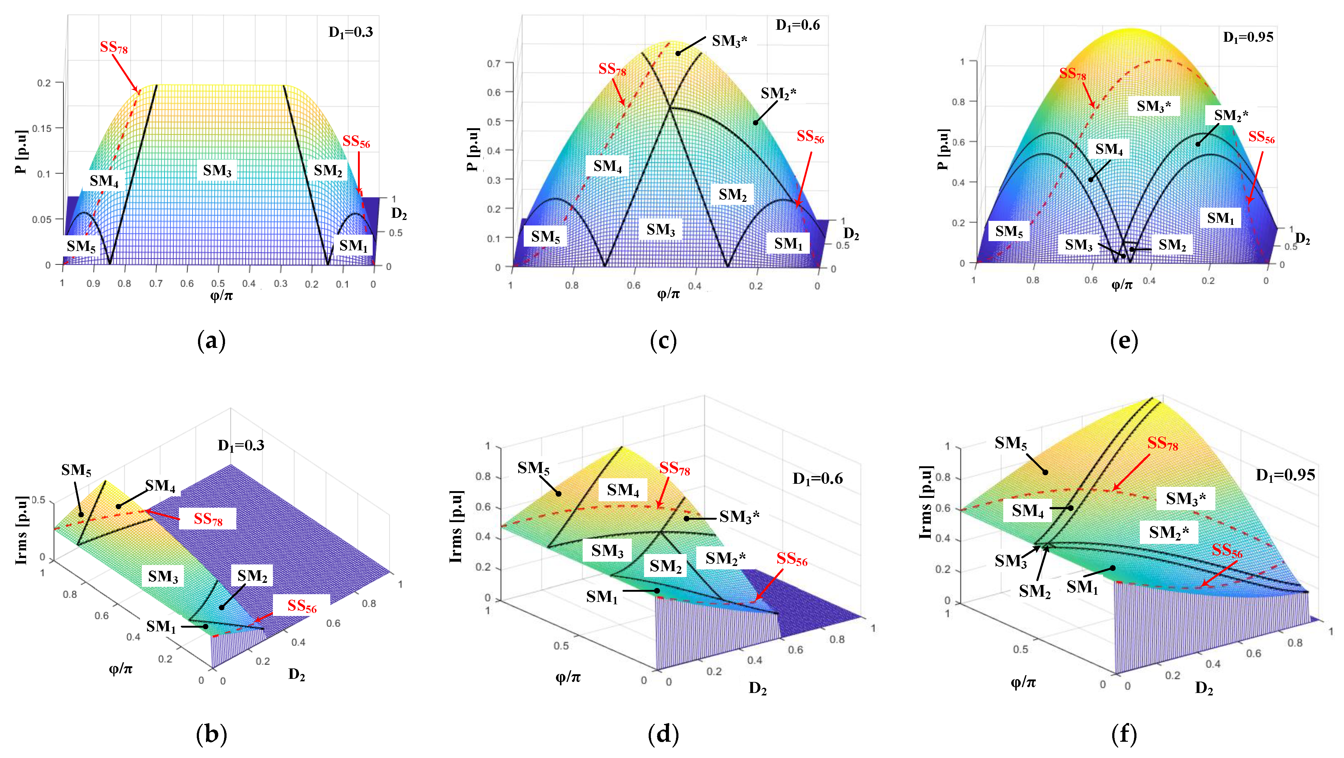
  • In Case I, only three (SM3*, SM4 and SM5) of the seven switching modes can achieve ZCS or ZVS for all the switches, although the only SM3* has a minimum inductor RMS current when D1 > 0.5. The remaining switching modes (SM1, SM2, SM2*, and SM3) operate with hard switching in a leg of bridge 2, since φ < SS56 (D1, D2) or φ < SS78 (D1, D2), see Table 5, Figure 8d,f.
  • In Case II, ZVS and ZCS are reached for all switching modes and the whole power range. For low and medium powers, soft switching is got by applying the expression in Equation (10) with D1 ≤ d and D2 < 1. High power is got either by operating in extending mode with D2 = 1 and D1 > d (EPS modulation), or with D2 = 1 and D1 =1 (PS modulation). For SM1, SM2, and SM2*, the lowest RMS current is obtained at the boundary between them, see Figure 10d for the same transferred power. For the highest power, SM3* achieves the lowest inductor RMS current.
A 250 W DAB experimental prototype has been built and tested in the laboratory to validate the theoretical analysis and the soft-switching conditions for the switching modes of Case I and Case II. In addition, the switching in each switch has been verified, for each switching mode.

Author Contributions

C.C. did theoretical analysis, derivation, circuit implementation, experimental testing, data processing and wrote the original draft paper. A.B. is the responsible for funding acquisition, supervision and administration, her contributions were related with the theoretical analysis, data analysis, and the paper reviewing and editing. A.R. wrote and reviewed the paper. P.A. contributed with theoretical analysis and with significant comments on the manuscript structure. A.L., C.F. and P.Z. reviewed and contributed with useful comments on the paper structure and mains paper contributions.

Funding

This research was funded by the Spanish Ministry of Economy and Competitiveness and ERDF, grant number DPI2014-53685-C2-1-R.

Acknowledgments

This work has been partially supported by the Spanish Ministry of Economy and Competitiveness and FEDER (ERDF), through the research project “Storage and Energy Management for Hybrid Electric Vehicles based on Fuel Cell, Battery and Supercapacitors”-ELECTRICAR-AG-(DPI2014-53685-C2-1-R).

Conflicts of Interest

The authors declare no conflicts of interest.

Nomenclature

V1DC voltage for bridge 1.dVoltage ratio.
V2DC voltage for bridge 2.vgxGate-source voltage for Mosfet “x”.
v11Output voltage of the Bridge 1.SMxSwitching mode “x”.
v22Input voltage of the Bridge 2.MxSwitch “x”.
D1Pulse width of v11.SSxySoft switching condition for MOSFET “x” and “y”.
D2Pulse width of v22.DABDual Active Bridge.
φPhase shift between v11 and v22.PSPhase shift.
fswSwitching frequency.SPSSimple Phase Shift.
TswSwitching period.DPSDual Phase Shift.
nTransformer turns ratio.TPSTriple Phase Shift.
LSeries inductor.EPSExtended Phase Shift.
iLInductor current.ZVSZero voltage switching.
VLInductor voltage.ZCSZero current switching.

References

  1. Yu, F.; Cao, S.; Xie, Y.; Wheeler, P. Study on bidirectional-charger for electric vehicle applied to power dispatching in smart grid. In Proceedings of the 2016 IEEE 8th International Power Electronics and Motion Control Conference, Hefei, China, 22–26 May 2016. [Google Scholar]
  2. Evzelman, M.; Ur Rehman, M.M.; Hathaway, K.; Zane, R.; Costinett, D.; Maksimovic, D. Active Balancing System for Electric Vehicles With Incorporated Low-Voltage Bus. IEEE Trans. Power Electron. 2016, 31, 7887–7895. [Google Scholar] [CrossRef]
  3. Xue, L.; Shen, Z.; Boroyevich, D.; Mattavelli, P.; Diaz, D. Dual Active Bridge-Based Battery Charger for Plug-in Hybrid Electric Vehicle with Charging Current Containing Low Frequency Ripple. IEEE Trans. Power Electron. 2015, 30, 7299–7307. [Google Scholar] [CrossRef]
  4. Mastromauro, R.A.; Poliseno, M.C.; Pugliese, S.; Cupertino, F.; Stasi, S. SiC MOSFET Dual Active Bridge converter for harsh environment applications in a more-electric-aircraft. In Proceedings of the 2015 International Conference on Electrical Systems for Aircraft, Railway, Ship Propulsion and Road Vehicles (ESARS), Aachen, Germany, 3–5 March 2015. [Google Scholar]
  5. Tariq, M.; Maswood, A.I.; Gajanayake, C.J.; Gupta, A.K. A Lithium-ion battery energy storage system using a bidirectional isolated DC-DC converter with current mode control for More Electric Aircraft. In Proceedings of the 2016 IEEE Symposium on Computer Applications & Industrial Electronics (ISCAIE), Batu Feringghi, Malaysia, 30–31 May 2016. [Google Scholar]
  6. Khan, M.M.S.; Faruque, M.O. Management of hybrid energy storage systems for MVDC power system of all electric ship. In Proceedings of the 2016 North American Power Symposium (NAPS), Denver, CO, USA, 18–20 September 2016. [Google Scholar]
  7. Xie, R.; Shi, Y.; Li, H. Modular multilevel DAB (M2DAB) converter for shipboard MVDC system with fault protection and ride-through capability. In Proceedings of the 2015 IEEE Electric Ship Technologies Symposium (ESTS), Alexandria, VA, USA, 21–24 June 2015. [Google Scholar]
  8. Rico-Secades, M.; Calleja, A.; Llera, D.G.; Corominas, E.L.; Medina, N.H.; Miranda, J.C. Cosine Phase Droop Control (CPDC) for the Dual-Active Bridge in lighting smart grids applications. In Proceedings of the 2016 IEEE International Conference on Industrial Technology (ICIT), Taipei, Taiwan, 14–17 March 2016. [Google Scholar]
  9. Yin, C.; Wu, H.; Locment, F.; Sechilariu, M. Energy management of DC microgrid based on photovoltaic combined with diesel generator and supercapacitor. Energy Convers. Manag. 2017, 132, 14–27. [Google Scholar] [CrossRef]
  10. Fathabadi, H. Novel wind powered electric vehicle charging station with vehicle-to-grid (V2G) connection capability. Energy Convers. Manag. 2017, 136, 229–239. [Google Scholar] [CrossRef]
  11. Pires, V.F.; Romero-Cadaval, E.; Vinnikov, D.; Roasto, I.; Martins, J.F. Power converter interfaces for electrochemical energy storage systems—A review. Energy Convers. Manag. 2014, 86, 453–475. [Google Scholar] [CrossRef]
  12. De Bernardinis, A. Synthesis on power electronics for large fuel cells: From power conditioning to potentiodynamic analysis technique. Energy Convers. Manag. 2014, 84, 174–185. [Google Scholar] [CrossRef]
  13. Amin, A.; Shousha, M.; Prodic, A.; Lynch, B. A transformerless dual active half-bridge DC-DC converter for point-of-load power supplies. In Proceedings of the 2015 IEEE Energy Conversion Congress and Exposition (ECCE), Montreal, QC, Canada, 20–24 September 2015; pp. 133–140. [Google Scholar]
  14. Alonso, A.R.; Sebastian, J.; Lamar, D.G.; Hernando, M.M.; Vazquez, A. An overall study of a Dual Active Bridge for bidirectional DC/DC conversion. In Proceedings of the 2010 IEEE Energy Conversion Congress and Exposition, Atlanta, GA, USA, 12–16 September 2010; pp. 1129–1135. [Google Scholar]
  15. Zhao, B.; Yu, Q.; Sun, W. Extended-Phase-Shift Control of Isolated Bidirectional DC–DC Converter for Power Distribution in Microgrid. IEEE Trans. Power Electron. 2012, 27, 4667–4680. [Google Scholar] [CrossRef]
  16. Wen, H.; Su, B. Operating modes and practical power flow analysis of bidirectional isolated power interface for distributed power systems. Energy Convers. Manag. 2016, 111, 229–238. [Google Scholar] [CrossRef]
  17. Lei, T.; Wu, C.; Liu, X. Multi-Objective Optimization Control for the Aerospace Dual-Active Bridge Power Converter. Energies 2018, 11, 1168. [Google Scholar] [CrossRef]
  18. Sun, C.; Li, X. Fast Transient Modulation for a Step Load Change in a Dual-Active-Bridge Converter with Extended-Phase-Shift Control. Energies 2018, 11, 1569. [Google Scholar] [CrossRef]
  19. Oggier, G.G.; GarcÍa, G.O.; Oliva, A.R. Switching Control Strategy to Minimize Dual Active Bridge Converter Losses. IEEE Trans. Power Electron. 2009, 24, 1826–1838. [Google Scholar] [CrossRef]
  20. Liu, X.; Zhu, Z.Q.; Stone, D.A.; Foster, M.P.; Chu, W.Q.; Urquhart, I.; Greenough, J. Novel Dual-Phase-Shift Control With Bidirectional Inner Phase Shifts for a Dual-Active-Bridge Converter Having Low Surge Current and Stable Power Control. IEEE Trans. Power Electron. 2017, 32, 4095–4106. [Google Scholar] [CrossRef]
  21. Malek, M.H.A.B.A.; Kakigano, H. Fundamental study on control strategies to increase efficiency of dual active bridge DC-DC converter. In Proceedings of the IECON 2015—41st Annual Conference of the IEEE Industrial Electronics Society, Yokohama, Japan, 9–12 November 2015; pp. 1073–1078. [Google Scholar]
  22. Calderon, C.; Barrado, A.; Rodriguez, A.; Lazaro, A.; Fernandez, C.; Zumel, P. Dual active bridge with triple phase shift by obtaining soft switching in all operating range. In Proceedings of the 2017 IEEE Energy Conversion Congress and Exposition (ECCE), Cincinnati, OH, USA, 1–5 October 2017; pp. 1739–1744. [Google Scholar]
  23. Calderon, C.; Barrado, A.; Rodriguez, A.; Lazaro, A.; Sanz, M.; Olias, E. Dual active bridge with triple phase shift, soft switching and minimum RMS current for the whole operating range. In Proceedings of the IECON 2017—43rd Annual Conference of the IEEE Industrial Electronics Society, Beijing, China, 29 October–1 November 2017; pp. 4671–4676. [Google Scholar]
  24. Chakraborty, S.; Tripathy, S.; Chattopadhyay, S. Minimum RMS current operation of the dual-active half-bridge converter using three degree of freedom control. In Proceedings of the 2016 IEEE Energy Conversion Congress and Exposition (ECCE), Milwaukee, WI, USA, 18–22 September 2016; pp. 1–8. [Google Scholar]
  25. Harrye, Y.A.; Ahmed, K.; Adam, G.; Aboushady, A. Comprehensive steady state analysis of bidirectional dual active bridge DC/DC converter using triple phase shift control. In Proceedings of the 2014 IEEE 23rd International Symposium on Industrial Electronics (ISIE), Istanbul, Turkey, 1–4 June 2014; pp. 437–442. [Google Scholar]
  26. Huang, J.; Wang, Y.; Li, Z.; Lei, W. Unified Triple-Phase-Shift Control to Minimize Current Stress and Achieve Full Soft-Switching of Isolated Bidirectional DC–DC Converter. IEEE Trans. Ind. Electron. 2016, 63, 4169–4179. [Google Scholar] [CrossRef]
  27. Xiong, F.; Wu, J.; Hao, L.; Liu, Z. Backflow power optimization control for dual active bridge DC-DC converters. Energies 2017, 10, 1403. [Google Scholar] [CrossRef]
  28. Krismer, F.; Kolar, J.W. Closed form solution for minimum conduction loss modulation of DAB converters. IEEE Trans. Power Electron. 2012, 27, 174–188. [Google Scholar] [CrossRef]
  29. Everts, J. Closed-Form Solution for Efficient ZVS Modulation of DAB Converters. IEEE Trans. Power Electron. 2017, 32, 7561–7576. [Google Scholar] [CrossRef]
  30. Riedel, J.; Holmes, D.G.; McGrath, B.P.; Teixeira, C. Maintaining Continuous ZVS Operation of a Dual Active Bridge by Reduced Coupling Transformers. IEEE Trans. Ind. Electron. 2018, 65, 9438–9448. [Google Scholar] [CrossRef]
  31. Zhao, B.; Song, Q.; Liu, W.; Sun, Y. Dead-Time Effect of the High-Frequency Isolated Bidirectional Full-Bridge DC–DC Converter: Comprehensive Theoretical Analysis and Experimental Verification. IEEE Trans. Power Electron. 2014, 29, 1667–1680. [Google Scholar] [CrossRef]
  32. Li, J.; Chen, Z.; Shen, Z.; Mattavelli, P.; Liu, J.; Boroyevich, D. An adaptive dead-time control scheme for high-switching-frequency dual-active-bridge converter. In Proceedings of the 2012 Twenty-Seventh Annual IEEE Applied Power Electronics Conference and Exposition (APEC), Orlando, FL, USA, 5–9 February 2012; pp. 1355–1361. [Google Scholar]
  33. Xu, F.; Zhao, F.; Shi, Q.; Wen, X. Researches on the Output Power Range of ZVS of Dual Active Bridge Isolated DC-DC Converters. In Proceedings of the 2018 IEEE Transportation Electrification Conference and Expo, Asia-Pacific (ITEC Asia-Pacific), Bangkok, Thailand, 6–9 June 2018; pp. 1–5. [Google Scholar]
Figure 1. DAB Topology.
Energies 11 02419 g001
Figure 2. Types of modulation applied to Dual active bridge (DAB). (a) Phase shift (PS); (b) Extended phase shift (EPS); (c) Dual phase shift (DPS); and (d) Triple phase shift (TPS).
Energies 11 02419 g002
Figure 3. Typical voltages and current for a Dual active bridge (DAB) with a Triple phase shift (TPS) modulation.
Energies 11 02419 g003
Figure 4. Case I: Switching modes for φ > 0. (a) SM1; (b) SM2, SM2*; (c) SM3; (d) SM4; (e) SM5, and (f) SM3*.
Energies 11 02419 g004
Figure 5. Case II: Switching modes for φ > 0. (a) SM1; (b) SM2, SM2*; (c) SM3; (d) SM4; (e) SM5, and (f) SM3*.
Energies 11 02419 g005
Figure 6. Switching modes. Case I: (a) SM2, SM2*, SM3*, and SM4; (b) SM1, SM3 and SM5; Case II: (c) SM2, SM2*, SM3*, and SM4; and (d) SM1, SM3 and SM5.
Energies 11 02419 g006
Figure 7. Case I (SM3*): ZVS and ZCS Analysis. Projections of the soft switching conditions and SM3* region onto the planes φ/π − D1 and φ/π − D2 (a) All soft switching conditions and SM3* region; (b) Projections for M1 and M2; (c) Projections for M3 and M4; (d) Projections for M5 and M6; (e) Projections for M7 and M8; and (f) Soft switching region (BGTV) for all switches. For this case d = 0.677.
Energies 11 02419 g007
Figure 8. Case I: Power and RMS current per unit [p.u] normalized to the maximum values, and switching modes for different D1 values when d = 0.677. (a) Power for D1 = 0.3; (b) RMS current for D1 = 0.3; (c) Power for D1 = 0.6; (d) RMS current for D1 = 0.6; (e) Power for D1 = 0.95; and (f) RMS current for D1 = 0.95.
Energies 11 02419 g008
Figure 9. Case II. Non-depending on φ conditions: (a) Switching modes for D1 ≤ d; and (b) Extended Switching Modes for D1 > d.
Energies 11 02419 g009
Figure 10. Case II for Extended Switching Modes (SM1, SM3*, SM5), d = 0.677. (a) Depending and Non-depending soft switching conditions; (b) ZVS and hard switching (HS) zones; (c) Power flow [p.u]; and (d) Inductor RMS current [p.u]. [p.u] is normalized to the maximum values.
Energies 11 02419 g010
Figure 11. Block diagram of the experimental circuit layout.
Energies 11 02419 g011
Figure 12. Switching modes for Case I: (a) SM1 with HS in M5 y M6 (φ/π < SS56); (b) SM2 with HS in M5 y M6 (φ/π < SS56); (c) SM2* with ZVS in M5 y M6 (φ/π > SS56); (d) SM3* with ZVS in M7 y M8 (φ/π > SS78); (e) SM4 with ZVS in M7 y M8 (φ/π > SS78); and (f) SM5 with HS in M7 y M8 (φ/π < SS78).
Energies 11 02419 g012
Figure 13. Switching modes for Case II: (a) SM1 for D1 = 0.44, D2 = 0.664, and φ/π = 0.048; (b) SM2 for D1 = 0.42, D2 = 0.656, and φ/π = 0.206; (c) SM3 for D1 = 0.132, D2 = 0.2, and φ/π = 0.458; (d) SM4 for D1 = 0.312, D2 = 0.34, and φ/π = 0.806; (e) SM5 for D1 = 0.221, D2 = 0.435, and φ/π = 0.896; (f) SM3* for D1 = 0.564, D2 = 0.838, and φ/π = 0.521.
Energies 11 02419 g013
Table 1. Boundaries for switching modes: Case I and Case II.
SMiCase ICase II
SM1 0 < φ ( D 1 D 2 2 ) · π 0 < φ ( D 2 D 1 2 ) · π
SM2 ( D 1 D 2 2 ) · π < φ ( D 1 + D 2 2 ) · π ( D 2 D 1 2 ) · π < φ ( D 2 + D 1 2 ) · π
SM2* ( D 1 D 2 2 ) · π < φ ( 1 D 1 + D 2 2 ) · π ( D 2 D 1 2 ) · π < φ ( 1 D 2 + D 1 2 ) · π
SM3 ( D 1 + D 2 2 ) · π < φ ( 1 D 1 + D 2 2 ) · π ( D 2 + D 1 2 ) · π < φ ( 1 D 2 + D 1 2 ) · π
SM3* ( 1 D 1 + D 2 2 ) · π < φ ( D 1 + D 2 2 ) · π ( 1 D 2 + D 1 2 ) · π < φ ( D 2 + D 1 2 ) · π
SM4 ( 1 D 1 + D 2 2 ) · π < φ ( 1 D 1 D 2 2 ) · π ( 1 D 2 + D 1 2 ) · π < φ ( 1 D 2 D 1 2 ) · π
SM5 ( 1 D 1 D 2 2 ) · π < φ < π ( 1 D 2 D 1 2 ) · π < φ < π
Table 2. Inductor current and output power for Case I and Case II.
SMiCurrentPower
Case ICase IICase ICase II
SM1 i L ( t 1 LH ) = i L ( t 1 HL ) = D 1 · V 1 · n D 2 · V 2 4 · L · f sw · n i L ( t 2 LH ) = D 2 · V 1 · n 2 · V 1 · ( φ / π ) · n D 2 · V 2 4 · L · f sw · n i L ( t 2 HL ) = D 2 · V 1 · n + 2 · V 1 · ( φ / π ) · n D 2 · V 2 4 · L · f sw · n i L ( t 1 LH ) = D 1 · V 1 · n 2 · V 2 · ( φ / π ) D 1 · V 2 4 · L · f sw · n i L ( t 1 HL ) = D 1 · V 1 · n + 2 · V 2 · ( φ / π ) D 1 · V 2 4 · L · f sw · n i L ( t 2 HL ) = i L ( t 2 LH ) = D 1 · V 1 · n D 2 · V 2 4 · L · f sw · n V 1 · V 2 · D 2 · ( φ / π ) 2 · L · f sw · n V 1 · V 2 · D 1 · ( φ / π ) 2 · L · f sw · n
SM2 i L ( t 1 LH ) = i L ( t 2 HL ) = D 1 · V 1 · n D 2 · V 2 4 · L · f sw · n i L ( t 1 HL ) = D 1 · V 1 · n + 2 · V 2 · ( φ π ) D 1 · V 2 4 · L · f sw · n i L ( t 2 LH ) = D 2 · V 1 · n 2 · V 1 · ( φ / π ) · n D 2 · V 2 4 · L · f sw · n V 1 · V 2 4 · L · f sw · n · [ φ π · ( D 1 + D 2 φ π ) ( D 1 D 2 ) 2 4 ]
SM 2 *
SM3 i L ( t 1 LH ) = i L ( t 2 HL ) = D 1 · V 1 · n D 2 · V 2 4 · L · f sw · n i L ( t 1 HL ) = i L ( t 2 LH ) = D 1 · V 1 · n + D 2 · V 2 4 · L · f sw · n V 1 · V 2 · D 1 · D 2 4 · L · f sw · n
SM 3 * i L ( t 1 LH ) = D 1 · V 1 · n + D 1 · V 2 2 · V 2 · ( 1 φ / π ) 4 · L · f sw · n i L ( t 1 HL ) = D 1 · V 1 · n D 1 · V 2 + 2 · V 2 · ( φ / π ) 4 · L · f sw · n i L ( t 2 LH ) = D 2 · V 1 · n D 2 · V 2 2 · V 1 · n · ( φ / π ) 4 · L · f sw · n i L ( t 2 HL T sw 2 ) = D 2 · V 1 · n + D 2 · V 2 2 · V 1 · n · ( 1 φ / π ) 4 · L · f sw · n V 1 · V 2 2 · L · f sw · n · [ φ π · ( 1 φ π ) ( D 1 1 ) 2 + ( D 2 1 ) 2 4 ]
SM4 i L ( t 1 LH ) = D 1 · V 1 · n + D 1 · V 2 2 · V 2 · ( 1 φ / π ) 4 · L · f sw · n i L ( t 1 LH ) = i L ( t 2 LH ) = D 1 · V 1 · n + D 2 · V 2 4 · L · f sw · n i L ( t 2 HL T sw 2 ) = D 2 · V 1 · n + D 2 · V 2 2 · V 1 · n · ( 1 φ / π ) 4 · L · f sw · n V 1 · V 2 4 · L · f sw · n · [ ( 1 φ π ) · ( D 1 + D 2 + φ π 1 ) ( D 1 D 2 ) 2 4 ]
SM5 i L ( t 1 LH ) = i L ( t 1 HL ) = D 1 · V 1 · n + D 2 · V 2 4 · L · f sw · n i L ( t 2 LH T sw 2 ) = D 2 · V 1 · n + D 2 · V 2 + 2 · V 1 · n · ( 1 φ / π ) 4 · L · f sw · n i L ( t 2 HL T sw 2 ) = D 2 · V 1 · n + D 2 · V 2 2 · V 1 · n · ( 1 φ / π ) 4 · L · f sw · n i L ( t 1 LH ) = D 1 · V 1 · n + D 1 · V 2 2 · V 2 · ( 1 φ π ) 4 · L · f sw · n i L ( t 1 HL ) = D 1 · V 1 · n + D 1 · V 2 + 2 · V 2 · ( 1 φ π ) 4 · L · f sw · n i L ( t 2 LH T sw 2 ) = i L ( t 2 HL T sw 2 ) = D 1 · V 1 · n + D 2 · V 2 4 · L · f sw · n V 1 · V 2 · D 2 · ( 1 φ / π ) 2 · L · f sw · n V 1 · V 2 · D 1 · ( 1 φ / π ) 2 · L · f sw · n
Table 3. Soft switching conditions for each switch.
SwitchZVSZCS
M1iL(t1LH) < 0iL(t1LH + Tsw/2) = 0
M2iL(t1LH + Tsw/2) > 0iL(t1LH) = 0
M3iL(t1HL) > 0iL(t1HL + Tsw/2) = 0
M4iL(t1HL + Tsw/2) < 0iL(t1HL) = 0
M5iL(t2LH) > 0iL(t2LH + Tsw/2) = 0
M6iL(t2LH + Tsw/2) < 0iL(t2LH) = 0
M7iL(t2HL) < 0iL(t2HL + Tsw/2) = 0
M8iL(t2HL + Tsw/2) > 0iL(t2HL) = 0
Table 4. Case I (v11 ≥ v22 and D1 > D2): General conditions to obtain Zero voltage switching (ZVS) and Zero current switching (ZCS) for each switch.
SMiSwitch
M1M2M3M4M5M6M7M8
SM1 D 1 · V 1 · n D 2 · V 2 D 1 · V 1 · n D 2 · V 2 φ [ D 2 2 · ( 1 V 2 V 1 · n ) ] · π φ [ D 2 2 · ( 1 V 2 V 1 · n ) ] · π
SM2 φ [ D 1 2 · ( 1 V 1 · n V 2 ) ] · π D 1 · V 1 · n D 2 · V 2
SM2*
SM3 D 1 · V 1 · n + D 2 · V 2 0 D 1 · V 1 · n + D 2 · V 2 0
SM3* φ [ 1 D 1 2 · ( 1 + V 1 · n V 2 ) ] · π φ [ D 1 2 · ( 1 V 1 · n V 2 ) ] · π φ [ D 2 2 · ( 1 V 2 V 1 · n ) ] · π φ [ 1 D 2 2 · ( 1 + V 2 V 1 · n ) ] · π
SM4 D 1 · V 1 · n + D 2 · V 2 0 D 1 · V 1 · n + D 2 · V 2 0
SM5 D 1 · V 1 · n + D 2 · V 2 0 φ [ 1 + D 2 2 · ( 1 + V 2 V 1 · n ) ] · π
Table 5. Case I (v11 ≥ v22 and D1 > D2): Type of switching and conditions to obtain ZVS and ZCS for each switch.
SMiRangeConditionType of Switching
M1M2M3M4M5M6M7M8
SM1 0 < φ ( D 1 D 2 2 ) · π SS 56   ( D 2 , d ) = D 2 2 · ( 1 d ) ZVSZVSZVS
φ/π > SS56 (D2,d)
ZCS
φ/π = SS56 (D2,d)
HS
φ/π < SS56 (D2,d)
HS
SM2 ( D 1 D 2 2 ) · π < φ ( D 1 + D 2 2 ) · π
SM2* ( D 1 D 2 2 ) · π < φ ( 1 D 1 + D 2 2 ) · π
SM3 ( D 1 + D 2 2 ) · π < φ ( 1 D 1 + D 2 2 ) · π Always fulfilZVS
SM3* ( 1 D 1 + D 2 2 ) · π < φ ( D 1 + D 2 2 ) · π SS 78   ( D 2 , d ) = ( 1 D 2 2 · ( 1 + d ) ) ZVS
φ/π > SS56 (D2,d)
ZCS
φ/π = SS56 (D2,d)
HS
φ/π < SS56 (D2,d)
ZVS
φ/π > SS78 (D2,d)
ZCS
φ/π = SS78 (D2,d)
HS
φ/π < SS78 (D2,d)
SM4 ( 1 D 1 + D 2 2 ) · π < φ ( 1 D 1 D 2 2 ) · π ZVS
SM5 ( 1 D 1 D 2 2 ) · π < φ < π
Table 6. Case II (v11 ≥ v22 and D1 ≤ D2): General conditions to obtain ZVS and ZCS for each switch.
SMiSwitch
M1M2M3M4M5M6M7M8
SM1 φ [ D 1 2 · ( 1 V 1 · n V 2 ) ] · π φ [ D 1 2 · ( 1 V 1 · n V 2 ) ] · π D 1 · V 1 · n D 2 · V 2 D 1 · V 1 · n D 2 · V 2
SM2 D 1 · V 1 · n D 2 · V 2 φ [ D 2 2 · ( 1 V 2 V 1 · n ) ] · π
SM2*
SM3 D 1 · V 1 · n + D 2 · V 2 0 D 1 · V 1 · n + D 2 · V 2 0
SM3* φ [ 1 D 1 2 · ( 1 + V 1 · n V 2 ) ] · π φ [ D 1 2 · ( 1 V 1 · n V 2 ) ] · π φ [ D 2 2 · ( 1 V 2 V 1 · n ) ] · π φ [ 1 D 2 2 · ( 1 + V 2 V 1 · n ) ] · π
SM4 D 1 · V 1 · n + D 2 · V 2 0 D 1 · V 1 · n + D 2 · V 2 0
SM5 φ [ 1 + D 1 2 · ( 1 + V 1 · n V 2 ) ] · π D 1 · V 1 · n + D 2 · V 2 0
Table 7. Case II (v11 ≥ v22 and D1 ≤ D2): Boundaries for each extended switching modes.
SMiCase II
SM1 0 < φ ( 1 D 1 2 ) · π
SM3* ( 1 D 1 2 ) · π < φ ( 1 + D 1 2 ) · π
SM5 ( 1 + D 1 2 ) · π < φ < π
Table 8. Case II (v11 ≥ v22 and D1 ≤ D2): Boundaries, power, and type of switching for each switch.
SMiRangePowerType of Switching
M1–M2M3–M4M5–M6M7–M8
D1 ≤ d
D2 = D1/d
SM1 0 < φ < D 1 ( d 1 ) 2 d π V 1 2 D 1 2 φ 2 L f sw D 2 π ZVSZVSZCSZCS
φ = D 1 ( d 1 ) 2 d π ZCS
SM2 D 1 ( d 1 ) 2 d π < φ < D 1 ( d + 1 ) 2 d π V 1 2 d 4 L f sw [ φ π ( D 1 d ( d + 1 ) φ π ) D 1 2 ( d 1 ) 2 4 d 2 ] ZVS
SM2* D 1 ( d 1 ) 2 d π < φ < 1 D 1 ( d + 1 ) 2 d π
SM3 D 1 ( d + 1 ) 2 d π < φ < 1 D 1 ( d + 1 ) 2 d π V 1 2 D 1 2 4 L f sw
SM3* ( 1 D 1 ( d + 1 ) 2 d ) π < φ D 1 ( d + 1 ) 2 d π V 1 2 d 2 L f sw [ φ π ( 1 φ π ) ( D 1 1 ) 2 + ( D 2 1 ) 2 4 ] ZVSZVS
SM4 ( 1 D 1 ( d + 1 ) 2 d ) π < φ ( 1 D 1 ( d 1 ) 2 d ) π V 1 2 d 4 L f sw [ ( 1 φ π ) ( D 1 d ( d + 1 ) + φ π 1 ) D 1 2 ( d 1 ) 2 4 d 2 ]
SM5 ( 1 D 1 ( d 1 ) 2 d ) π < φ π V 1 2 D 1 ( 1 φ π ) 2 L f sw
D1 > d
D2 = 1
SM1 0 < φ ( D 1 1 2 ) π V 1 2 D 1 2 φ 2 L f sw π ZVSZVSHSHS
SM3* ( 1 D 1 2 ) π < φ < ( 1 d 2 ) π V 1 2 d 2 L f sw [ φ π ( 1 φ π ) ( D 1 1 ) 2 4 ]
φ = ( 1 d 2 ) π ZCSZCS
( 1 d 2 ) π < φ < ( 1 + D 1 2 ) π ZVSZVS
SM5 ( 3 D 1 2 ) π < φ π V 1 2 D 1 ( 1 φ π ) 2 L f sw
Table 9. DAB parameters.
DescriptionsSpecifications
Port 1 Voltage V136 V
Port 2 Voltage V272 V
Transformer turns ratio: 1:n1:3
Inductance: L3.88 μH
Switching frequency: fsw100 kHz
Port 1 capacitor: C160 μF
Port 2 capacitor: C260 μF

