Article

Dual 3-Phase Bridge Multilevel Inverters for AC Drives with Voltage Sag Ride-through Capability

by
Vitor Fernão Pires
1,2,
Joaquim Monteiro
2,3,* and
José Fernando Silva
2,4
1
SustainRD, EST Setubal, Polytechnic Institute of Setúbal, 2914-761 Setúbal, Portugal
2
INESC-ID, 1000-029 Lisboa, Portugal
3
ISEL—Polytechnic Institute of Lisboa, 1959-007 Lisboa, Portugal
4
IST—Instituto Superior Técnico, Universidade de Lisboa, 1049-001 Lisboa, Portugal
*
Author to whom correspondence should be addressed.
Energies 2019, 12(12), 2324; https://doi.org/10.3390/en12122324
Submission received: 22 May 2019 / Revised: 11 June 2019 / Accepted: 11 June 2019 / Published: 18 June 2019
(This article belongs to the Section F: Electrical Engineering)

Abstract

:
One of the main power quality issues that can affect variable speed drives (VSDs) is the occurrence of voltage sags on their AC power supply. Voltage sags can affect the inverter nominal operation, leading to a malfunction of the AC motor. This paper presents an inverter with resilient capability to voltage sags. The topology consists of two conventional three-phase bridge inverters arranged to require just a single DC source. This inverter is also characterized by a voltage multilevel operation, providing the full advantages of multilevel converters without the need for level balancing. Associated with this AC motor driver, a control system based on a field-oriented controller with a vector voltage modulator that will enable voltage sag ride-through capability is proposed. The proposed control system does not require any changes in the occurrence of voltage sags. To verify the characteristics of the proposed drive and control system, simulation tests are provided. Simulation results confirm the voltage sag resilient capability of the proposed multilevel converter.

1. Introduction

A major issue in industry applications is related to the power quality in the AC electrical grids [1]. In fact, due to the lack of AC power quality, important and costly losses in several industrial and business companies have been reported [2]. Among several power quality issues, one of the most hazardous is the occurrence of sags in the AC voltages [3]. This type of perturbation is normally originated by line faults or by sudden over-currents in the distribution lines, decreasing the AC voltage RMS value below 90% of the rated value and lasting from one AC grid cycle to few seconds. In fact, the Institute of Electrical and Electronics Engineering (IEEE) has a standard, numbered by 1159–1995, that defines voltage sag as “a decrease of 0.9 to 0.1 pu in the effective nominal voltage of half a cycle to 1 min duration” [4]. There is also another standard from a different institution, as is the case of the International Electrotechnical Commission (IEC). In this case, the definition of a voltage sag is given by the standard IEC 1000-2-1 [5], which is a sudden reduction of the voltage at a point in the electrical system, followed by a voltage recovery after a short period of time (from 0.5 cycle to a few seconds).
The variable speed drive (VSD) is a very important piece of industry equipment that can be severely affected by voltage sag perturbations, since AC drives are constant power loads. Most VSDs have power converters to drive three-phase induction motors. The typical topology used in VSDs includes a three-phase bridge diode rectifier, which provides a DC bus voltage to a single three-phase voltage source inverter (VSI) feeding the AC motor. The main disadvantage of this VSD is that it is very sensitive to voltage sags and short interruptions. In fact, the AC voltage RMS value decreased during the sag leads to the decrease of the DC bus voltage, which is no longer enough to drive the motor, causing a reduction of the speed/torque, motor overheating, or even a motor stoppage. In this way, several standards appear to allow VSD manufactures to test their equipment regarding voltage sags. The most important standards are the SEMI F47-0706 [6], the IEC 61000-4-34 [7], and the unbalance requirements of the IEC 61800-3 [8].
To analyze the impact of the several types of voltage sags, several studies have been published. In [9], a study was presented about the impact of sag disturbances on the DC-link inductor and DC bus electrolytic capacitors. A study about the impact on the VSD, taking into consideration the location of the inductor in the topology of the VSD, was presented in [10]. In [11], the impact of different types of voltage sags on an induction motor was analyzed. Several other studies were published [12,13,14,15,16,17]. To attenuate the sag issue, several solutions were used and proposed. One of the solutions uses a large DC capacitor or even a battery [18]. The use of a chopper connected to the DC bus was also proposed [19]. An active solution was also proposed, especially for a permanent-magnet synchronous generator (PMSG) connected to grid via back-to-back inverters for wind energy generation [20]. Another active solution for a motor AC drive was through the use of an active rectifier with an adequate control system [21]. However, these solutions are costly, have limited lifetimes (DC electrolytic capacitors or batteries), and/or are dependent on the voltage sag level and duration. In [22] another topology is presented to improve the voltage through the AC drive. However, this solution requires an extra DC-DC converter that increases the cost, losses, and complexity of the system. Another solution was proposed by [23], but, in this case, a single-stage three-phase boost inverter is used. This topology needs no extra switches, but requires extra passive components, such as inductors and capacitors. One of the aspects that can affect the performance of the drive regarding voltage sags is related to the capacitors. Higher capacitance values lead to better performance. This aspect was analyzed in works such as [10,24], namely regarding the use of supercapacitors. In [10] the use of the supercapacitors with an extra power converter was also considered. However, this also increases the complexity and cost of the system. Another aspect that should be considered in the design of the ASD drive is the allocation of the inductor to attenuate the current harmonics. In [25] the use of the AC or DC inductor was studied. It was shown that the performance of the two ASD configurations are almost identical if the inductance of the DC bus choke inductor is twice the value of each line inductor. Therefore, the line inductors affect the voltage sag capability of the drive since there is a voltage drop in the inductors.
Besides the classical two-level VSIs, the use of power electronic converters with multilevel output AC voltages was also proposed. Multilevel topologies present several advantages over the 3-phase two-level inverter [26]. Several multilevel topologies have been proposed to be used in AC VSDs, being the most known and studied flying capacitor-based inverter, including the Neutral-Point-Clamped (NPC) and the cascaded H-bridge inverter [27,28,29]. The third solution has the advantage of using simple single-phase two level VSIs. However, this solution requires a significant number of DC voltage sources. A solution that was used to overcome the problem of voltage sags based on a similar approach to the cascaded H-bridge inverter but that does not require DC voltage sources was proposed in [30]. In this approach, three single-phase inverters with a floating capacitor connected between the grid and the motor were used. However, this system presents a limitation in regards to their application to the VSIs, since does not allow for changing the frequency of the voltage applied to the motor. To obtain multilevel inverters using just well-known three-phase two-level VSIs, a new topology was proposed in [31], where the motor windings, in open-end configuration, are connected to two three-phase VSIs, each one at one side of the windings. However, this structure has the disadvantage of requiring two DC voltage sources. Using the open-end windings and two 3-phase VSIs, several works have been presented, proposing several control and modulation methods [32,33,34]. Based on the usage of motors with open-end windings and two 3-phase VSIs, other topologies, such as the ones presented in [35,36], were developed. To reduce the cost of the multilevel inverters, a dual three-phase VSI with a single DC voltage source was also proposed [37]. In this case, a DC capacitor is used at the DC terminals of one the three-phase VSIs. This topology is designated as a dual inverter with a floating capacitor.
Although open-end windings and two 3-phase VSIs topologies present several advantages over the single 3-phase VSI solution, very few studies have been made regarding the voltage sags issue and the possible advantages/disadvantages, namely the sag ride-through capability of the open-end windings dual inverter topology when subjected to voltage sags and similar disturbances. In fact, the previous works have usually been focused on the voltage boost capability of the rectifier (in VSDs with back-to-back inverters). However, due to the limitation of the boost gain, this solution presents limits regarding the decrease of the source voltage. As said before, many of the solutions require extra components, which increase the cost, complexity, and efficiency of the system. Therefore, to provide a better voltage sag ride-through capability in VSDs, this paper proposes the use of open-end windings and dual VSI structure for the AC VSD. This solution does need any extra power converter or components. To minimize the DC voltage source count and at the same time the referred voltage sags ride-through, only one of the 2 inverters is connected to the DC supply. Therefore, the two inverters may be operated in an asymmetrical regime. Besides the boost capability of the rectifier, there is also the capability to boost the floating capacitor voltage. Taking this into consideration, in this work, the capability to change the reference value for the floating capacitor voltage is also explored as a way to achieve a higher immunity to deep voltage sags. The proposed multilevel topology and controller allows boost operation without any extra converters or components. Another aspect of the topology regards the design aspects of the converter. In this case, since the topology presents boost capability, the voltage droop associated with the inductors used as filters is not critical in this system. Regarding the capacitors, their capacitance is also not critical due to that capability, although some stored energy is needed to be voltage sag resilient. Capacitors can be designed considering only the limitation of the ripple function of the switching frequency and load as usually is done in VSDs with the capability to ride-through voltage sags. A control system is also proposed for the two 3-phase VSIs with open-end windings and designed to maintain motor operation conditions during the occurrence of voltage sags. Associated with this control system, the use of a voltage vector modulator is proposed. In this context, the impact of the voltage vectors under several references of the floating voltage capacitor is also addressed. The performance of AC VSDs fitted with the dual VSI structure is tested through several simulation tests.

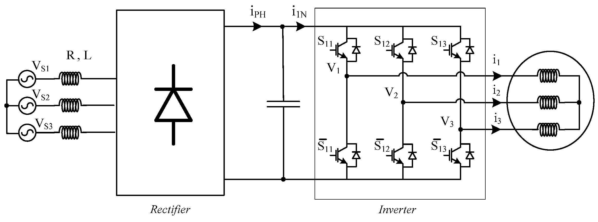
2. AC VSD with a Multilevel Inverter Based in Dual 3-Phase VSIs

2.1. Proposed Multilevel Inverter with Voltage Sag Ride-through Capability

Conventional VSDs for three-phase AC motors are based on a three-phase two-level VSI supplied by a full-bridge diode rectifier (Figure 1). The diode rectifier has no control over the DC bus voltage. Therefore, the DC voltage level is strongly dependent on the AC voltage RMS value, the VSDs performance being highly dependent on the DC-link voltage, since industrial AC motors give little margin to the DC Bus voltage variation. This fact makes existing VSDs very sensitive to voltage sags. Furthermore, the single inverter topology is also limited by the number of voltage levels that can be applied to the motor, imposing a high rate of rise of applied voltage in the motor windings. This section presents a circuit configuration to achieve the voltage sag ride-through capability. Figure 2 shows the proposed configuration, where the motor has open-end windings. Two 3-phase VSIs are connected to each side of the windings. One 3-phase VSI is DC fed from to the diode bridge rectifier while the second 3-phase VSI is connected to a DC floating capacitor. This capacitor enables the use of a single DC source (the diode bridge rectifier). This DC floating capacitor will be charged by the DC source constituted by the diode bridge rectifier and through the inverter that is directly connected to that source. Thus, proper control of the two inverters is essential to charge/discharge the floating capacitor, as is shown in next section.

2.2. Comparison with Other Topologies

As described in the introduction, several solutions have been proposed to eliminate or attenuate the problem of the voltage sags in AV VSDs. To point out the differences between existing solutions and the herein proposed topology and impact in the drives, Table 1 lists several characteristics, enabling comparisons. In the classical AC VSD structure, the immunity to voltage sags is clearly dependent of the storage element. Since the capacitor used in these drives usually does not have the required capacitance for sag ride-through, the sag immunity of the drive is very low. Thus, solutions using supercapacitors or batteries have also been proposed. Besides the cost of these storage elements, in some solutions the use of an extra power converter was also proposed, which further increases the system cost. Another solution was presented in [22], which uses a DC-DC buck-boost converter after the diode rectifier. However, this solution requires extra power semiconductors, higher voltage capacitors, and an extra storage element (inductor). To avoid the extra DC-DC converter, but still presenting boost capability, the use of an active rectifier (back-to-back inverter) was also proposed. This may give high immunity to voltage sag. However, it requires extra switches and depends on the control speed of the rectifier side. To provide multilevel capability to the AC VSD, the ABB company introduced a new multilevel topology [38]. This drive was named as ACS 200 and is characterized by ride-through functionality. However, this topology requires an important number of extra switches and capacitors. The herein proposed solution is also characterized by their multilevel operation. Nevertheless, it only requires an extra two-level three-phase inverter with a floating capacitor. It presents boost capability, even if used with a diode rectifier. It also can be used with an active rectifier, and, in this case, there are two converters with Boost capability, the rectifier and the inverter. In this way, the herein proposed topology will present a very high immunity to voltage sags.

2.3. AC VSD Model with the Proposed Multilevel Inverter

The model of the AC VSD presented in Figure 2 can be obtained considering that the power switches of each leg are defined as S i j and S ¯ i j , where I represents each of the inverters (1, 2) and j represents each of the legs (1, 2, or 3). Considering ideal power switches, the variables representing their switching states can be binary quantities. Consequently, it will be considered S = 1 when the switch is conducting (ON state mode) and S = 0 when the switch is turned OFF. Thus, in accordance with this and from the analysis of the converter power circuit, the AC voltages of the VSD (applied to each of the motor winding) are functions of the switches’ states, S i j , and DC voltages, VDC1, VDC2.
[ V 11 V 22 V 33 ]   =   V D C 1 [ 2 3 1 3 1 3 1 3 2 3 1 3 1 3 1 3 2 3 ]   [ S 11 S 12 S 13 ]      V D C 2 [ 2 3 1 3 1 3 1 3 2 3 1 3 1 3 1 3 2 3 ]   [ S 21 S 22 S 23 ]
From the analysis of Equation (1), supposing VDC1 = VDC2 = VDC and considering all the combinations of the switches, it is possible to obtain all the multilevel output voltages applied to each of the windings. The maximum voltage is 1.333 VDC, higher than the VDC voltage, therefore allowing some margin for handling voltage sags.
In order to obtain a vector representation of the multilevel inverter AC voltages in the αβ0 system coordinates, a Cark–Concordia transform is used. Thus, applying this transformation [39] (multiplying by Equation (2)) to the three-phase stationary coordinate system presented in (1), the new quantities will be expressed by Equation (3).
[ v α v β ]   = 2 3   [ 1 1 2 1 2 0 3 2 3 2 ]   [ V 11 V 22 V 33 ] .
[ V α V β ]   =   V D C 1 [ 2 3 1 6 1 6 0 1 2 1 2 ]   [ S 11 S 12 S 13 ]    + V D C 2 [ 0 0 0 1 0 1 0 1 1 ]   [ S 21 S 22 S 23 ] .
From this equation, and taking into consideration the states of the switches, it is possible to obtain the control system and the voltage vectors that will be used to develop a space-vector modulator for this VSD, as presented in the next section.

3. Control System

3.1. Field Oriented Control

The behavior of the wound-rotor induction motor can be described by the following equations, written in a reference frame synchronous with the rotor flux:
u ¯ s = r s i ¯ s + d ψ ¯ s d t + j ω r ψ ¯ s ,
u ¯ r = r r i ¯ r + d ψ ¯ r d t + j ( ω r ω ) ψ ¯ r ,
ψ ¯ s = L s i ¯ s + L m i ¯ r ,
ψ ¯ r = L r i ¯ r + L m i ¯ s ,
T = 3 2 p i ¯ r . j ψ ¯ r ,
where u ¯ s and u ¯ r denote the stator and rotor voltage, respectively; ψ ¯ s and ψ ¯ r represent the stator flux and rotor flux respectively; i ¯ s and i ¯ r are the stator and rotor currents; r s and r r are the stator and rotor resistances; L s , L r , and L m are the stator, rotor, and mutual inductances; ω r is the angular speed of the rotor flux vector; and ω is the rotor angular speed in electric radians.
One of the linear strategies most widely applied in power electronics is the field-oriented control principle (FOC) [40]. This control technique uses an appropriate coordinate system that allows the torque, T, and the flux, ψ ¯ r , to be controlled independently of each other. In rotor flux oriented synchronously rotating reference frame, the rotor flux is controlled by the real part of the stator current, i s d , and the torque by the imaginary part of the stator current, i s q . Therefore, Equations (9) and (10) represent the stator currents references ( i s d * and i s q * ) that are function of the flux ( ψ r * ) and torque (T) references, as follows:
i s d * = ψ r * L m ,
i s d * = L m L m T * ψ r * .
The location of the flux vector can be obtained by a simple velocity observer ( ω ^ ), which is obtained by the measure of the rotor rotation speed ( ω r ), (11).
ω ^ = ω r + L m τ r i s q * ψ r * .
These are the basic principles of FOC, their equations were implemented through Simulink blocks. The induction motor parameters have been obtained by manufacturer’s catalogue, given in the table that is presented in the results Section 5.

3.2. Current Controller

As previously verified, the controller of the motor requires the control of the stator currents in dq coordinates. In this way, a sliding mode current controller can be adopted defining sliding surfaces Sd and Sq as follows:
{ S d ( e i d , t )   =   k   ( i s d * i d )   = 0 S q ( e i q , t )   =   k   ( i s q * i q )   = 0   ,
where k is a positive definite constant. To ensure that the system reaches the sliding surface, to track the output reference current, a voltage vector modulator in the αβ plane is devised. To work on αβ coordinates, transformed switching functions that consider the currents in the αβ coordinates are defined as follows:
{ S 1 ( e i α , t )   =   k α   ( ( i s d * cos ( ω t ) i s q * sin ( ω t ) ) i α )   = 0 S 2 ( e i β , t )   =   k β   ( ( i s q * cos ( ω t ) + i s d * sin ( ω t ) ) i α )   = 0   ,
where kα, kβ are positive definite constants selected to limit the switching frequency of semiconductors.
The two sliding surfaces are used to select a voltage vector using a modulator. The modulator will ensure that the system trajectory will always move to the sliding surface and will stay in that surface, accordingly to the stability condition S ( e α , β , t )   S ( e α , β , t )   < 0 [41,42]. So, the vector modulator must be designed in order to choose a vector, taking into consideration the sliding surface (4) and the stability condition. For example, if S ( e α , t )   < 0 this means that ( i s d * cos ( ω t ) i s q * sin ( ω t ) ) < i α , then the chosen voltage vector must ensure S ( e α , t )   > 0 , which means using a vector with a positive component α and with sufficient amplitude.
To develop the required vector modulator, an analysis of the voltage vectors that the inverter can apply to the load must be performed. Thus, from Equation (3) and taking into consideration the six legs of the two inverters, there are 64 possible combinations. The amplitude and number of different voltage levels are functions of the DC voltages (VDC1 and VDC2). Considering that the DC voltages are equal, then 19 different voltages are obtained, as presented in Figure 3 (it was considered that the DC voltage has a value of 1 pu).

3.3. Impact of a Voltage Sag on the Voltage Vectors

To analyze the impact of a voltage sag on the voltage vectors that can be applied to the motor, a reduction of the VDC1 must be considered. It should be noted that, due to the structure of this topology, it is possible, through the development of an appropriate vector modulator, to maintain the voltage level of the floating capacitor (VDC2). Thus, considering a voltage sag of 20% (20% reduction in VDC1), the amplitude of the voltage vectors will also be affected (Figure 4a). In fact, in this situation, the amplitude of the vectors will be reduced. For example, for the vector with a higher amplitude (for example the one located in the rightmost point) the amplitude in the αβ plane will be reduced from 1.633 to 1.469. Another impact of this reduction is that, since the two DC voltages are not equal anymore, then the number of different voltage vectors will became higher (from 19 to 49). As expected, a further reduction of the VDC1 voltage will also further reduce the amplitude of the voltage vectors. Figure 4b shows the obtained voltage vectors for a voltage sag of 50%. In this case, the vector with a higher amplitude is decreased from 1.633 to 1.224. One of the aspects associated with this topology is that the reduction of the voltage vector amplitude is not proportional to the reduction of the DC voltage associated with the grid. In reality, it is much more attenuated since, with this topology, it is possible to maintain the voltage level across the floating capacitor (VDC2).
One characteristic of the dual VSI topology is the possibility of having higher voltages across the floating capacitor than the one associated with the DC source connected to the grid. Then, it is possible to compensate the reduction of the DC voltage originated by the grid. To verify this characteristic, an analysis of the increase of the voltage across the floating capacitor proportional to the reduction of the voltage of the DC source connected to the grid is also presented. In Figure 5a) is presented the obtained voltage vectors when there is a voltage sag of 20% (20% reduction in VDC1) and an increase by 20 % of the floating capacitor voltage (VDC2). Another example can be seen in Figure 5b) where is presented the obtained voltage vectors when there is a voltage sag of 50% and an increase by 50 % of the floating capacitor voltage (VDC2). From both figures is possible to verify that with the increase of the floating capacitor voltage (VDC2) is possible to compensate the reduction of the DC voltage associated to the rectifier. In fact, through this strategy the amplitude of the vectors with a higher amplitude is maintained.
Besides the control of the VSD AC voltages, the balance of the floating capacitor voltage (VDC2) must also be ensured. To ensure this balance without affecting the control of the VSD AC voltages, the redundant vectors will be used. In fact, the redundant vector choice enables higher voltages than the ones generated by the usual DC voltage. According to the required voltage, the switching combination that must be chosen among the redundant vectors is a function of the sign of the three-phase motor currents. Therefore, six sectors are defined in accordance with the following condition:
{   i 1 > 0      a n d    i 2 < 0   a n d    i 3 > 0       S e c t o r   I   i 1 > 0      a n d    i 2 < 0   a n d    i 3 < 0       S e c t o r   I I   i 1 > 0      a n d    i 2 > 0   a n d    i 3 < 0       S e c t o r   I I I   i 1 < 0      a n d    i 2 > 0   a n d    i 3 < 0       S e c t o r   I V   i 1 < 0      a n d    i 2 > 0   a n d    i 3 > 0       S e c t o r   V   i 1 < 0      a n d    i 2 < 0   a n d    i 3 > 0       S e c t o r   V I
As said, the regulation of the voltage across the floating capacitor is ensured by the redundant vectors. As an example, let’s consider VDC1 = VDC2 and that under the point of view of the load control the choice must be one of the vectors 2, 20, 38, 49, 56, and 58 (all these vectors maintain the same voltage components, as can be seen in Figure 3). Table 2 shows the switching combination and applied voltage. Thus, if the voltage of the floating capacitor is lower than the reference and the load currents are in sector I, then the voltage vector that will be adopted to ensure the charge of the floating capacitor is 38. Otherwise, if the voltage of the floating capacitor is higher than the reference, then the adopted voltage vector should be the 20.
The previous example can be seen through Figure 6. The condition of the switches and direction of the currents regarding vector 38 is shown in Figure 6a. Through this figure it is possible to verify that the output DC current of the right placed inverter flows in a way that the floating capacitor will be charged. However, if vector 20 is selected instead of vector 38, the direction of the output DC current of the rightmost inverter will be reversed, by which the floating capacitor will be discharged, as presented by Figure 6b.
Under the occurrence of a voltage sag there will be an asymmetry the DC voltages of the inverters, increasing the number of different voltage vectors, as shown in Figure 4. Thus, considering that VDC1 reduces to 80% of their nominal value, it is possible to now verify that all the previous vectors do not present the same amplitude as seen by Figure 4a and Table 3. However, their amplitude and location are very near, making it possible to maintain the same strategy, previously described (for sector I, if the voltage of the floating capacitor is lower than the reference then the adopted voltage vector should be the 38, otherwise, it must be chosen the vector 20).
During the voltage swell there is also an asymmetry of the DC inverter voltages. However, as in the case of the voltage sag, their amplitude and location are very nearly possible, even in this situation, to maintain the same strategy for the vector modulator.

3.4. Voltage Vector Modulator Implementation

As said before, the vector voltage modulator should be coordinated with the sliding surfaces of the motor controller. Thus, to establish a relationship between the vector to chosen and the control laws, several levels will be used, defined by a multilevel comparator. Since there are more different vectors in the α axis, when compared with the β axis, seven voltage levels for the law, associated with the α component, and five voltage levels for the β component are used (Figure 7). In accordance with the output of the comparators, the vector voltage to be applied is chosen. For example, considering that both components of the currents are much lower than the reference value, in this situation, the sliding surfaces (4) will give a high positive value. In this way, the vector with higher amplitude should be chosen. In a more generic way, the choice of the vector function of the sliding surfaces of the controller can be implemented through a look-up table, as presented in Table 4.

4. Simulation Results

To validate the proposed AC VSD and control system able to provide voltage sags ride-through, several digital computer simulations were performed. The simulation of the system was implemented in the program MATLAB/Simulink. The tests were performed on a 15 kW, 1445 rpm, 4-pole, and 50 Hz open-end winding induction motor. The induction motor parameters are given in Table 5 (they have been obtained by manufacturer’s catalogue). Regarding the parameters used for the grid and power converter, they are presented in Table 6. The values of the capacitors were selected in accordance with capacitances needed in classical AC drives, with a diode rectifier and an inverter with some voltage sag resiliency.
To analyze the voltage ride-through capability of the proposed system, a test is performed where the VSD dual 3-phase VSIs work with the nominal grid voltage and then a voltage sag occurs. At the output of the of the diode rectifier, the voltage (VDC1) is near the maximum of the phase-phase grid voltage. Since, in this case, the grid phase-neutral voltage is 230 V, their voltage is near 550 V. For the voltage of the floating capacitor (VDC2), a reference of 550 V was defined. The choice of this reference was made in order to work with symmetric DC voltages in normal situations (voltage vectors given by Figure 3). In this test, the grid voltage decreases suddenly, from 100% of the nominal voltage (Vn) to 70% Vn at t =1.5 s and back to 100% Vn at t = 2.2 s. Figure 8 presents the time behavior of the waveforms of the DC sides of the two inverters. As can be seen, although the voltage of the DC side connected to the grid is affected, the voltage in the DC side connected to the floating capacitor is not affected and stays constant. This creates immunity to the voltage sags in the system. In fact, through Figure 9 it is possible to confirm that the three-phase motor currents will not be affected by this voltage sag. The multilevel voltage applied to winding 1 of the motor is presented in Figure 10. This figure shows that the multilevel voltage is maintained even during the voltage sag, in spite of the existence of the reduction of their amplitude. It should be stated that the control system and modulation was not changed during the voltage sag.
Another similar test was made, but in this case the grid voltage decreased suddenly from 100% of the nominal voltage (Vn) to 30% Vn at t = 1.5 s and back to 100% Vn at t = 2.2 s. The time behavior of the waveforms of the DC sides of the two inverters is presented in Figure 11. In this case, it is possible to verify that voltage sags with very high depths lead to a high ripple in the voltage in the DC side connected to the floating capacitor. The voltage of the DC side connected to the grid is also strongly affected and also presents a high ripple. In this situation, the three-phase motor currents will be affected, as shown by Figure 12. This is due to the reduction of the available voltage that can be applied to the motor windings. In fact, due to this reduction, in this case the voltage is not enough to maintain the required amplitude of the currents. The multilevel voltage applied to winding 1 of the motor maintains their multilevel operation but with a higher reduction in their amplitude (Figure 13), confirming the cause for why the currents will not achieve the required value. However, this situation can be corrected by increasing the floating capacitor voltage, as shown in the next test.
In this test, the same conditions of the previous one were considered (same voltage sag, i.e., with a suddenly decrease of the voltage grid from 100% of the nominal voltage (Vn) to 30% Vn at t = 1.5 s and back to 100% Vn at t = 2.2 s), but in this case the reference of the floating capacitor voltage was changed. Thus, at t = 1.5 s, when the voltage sag occurs, the reference of the floating capacitor voltage was increased from 550 V to 650 V. The result of this test can be seen in Figure 14, which shows the time behavior of the waveforms of the DC sides of the two inverters. From this result it is possible to verify that the voltage in the floating capacitors will follow the reference and is stable all the time (maintaining a low voltage ripple). Moreover, it also shows the fast response to the sudden change in their reference. Regarding the three-phase currents, it is possible to verify that, in this case, they will not be affected as in the previous test (Figure 15). This is due to the fact that the voltage applied to the windings is higher than the previous case, since the voltage in the floating capacitor has increased. This can be seen in Figure 16, wherein the multilevel voltage applied to winding 1 of the motor is presented.

5. Conclusions

This work addressed the issue of voltage sags in AC VSDs with open-winding motors. To provide voltage sag ride-through capability, a multilevel inverter was proposed based in a Dual 3-phase VSIs structure connected to both sides of the open-end motor windings. The multilevel inverter uses two 3-phase VSIs, but requires only a single DC source. A three-phase diode rectifier connected to the grid is used as the DC source, while a floating capacitor is used in the other 3-phase VSI. This topology allows higher voltages in the floating capacitor, when compared to the voltage at the output of the diode rectifier. Due to the increase of this voltage, it is possible to obtain immunity to deep voltage sags. This characteristic cannot be completely achieved by the classical AC drives as the boost function is not possible. The controller used for the VSD is based in the field oriented control. To control the motor flux and torque, a sliding mode controller for the AC currents was also proposed and its outputs were used to select vectors from a voltage vector modulator. The analysis of the space vectors gave the margins to obtain voltage sag ride-through capability. The proposed system does not require changing the controller when voltage sags occur, but just needs an increase of the voltage in the floating capacitor to achieve resiliency to deep voltage sags. The demonstration of the capabilities of the proposed VSD and the control system was made through several simulation test cases with a 15-hp motor. The obtained results confirm the immunity capabilities and requirements to successfully ride-through deep voltage sags. These tests were made without changing the control or modulation strategy. The results show that to obtain a ride-through voltage sag capability, just an increase in the floating capacitor voltage is needed. The results also show that, even with a voltage sag of 70%, the system has the capability to maintain the required current of the motor. This property can only be obtained through the capability of the system to increase the voltage to the floating capacitor during the voltage sag.

Author Contributions

V.F.P. conceived the theory; V.F.P. and J.M. designed, implemented and performed the experiments; V.F.P., J.M. and J.F.S. analysed the data and wrote the paper.

Funding

This research was funded by national funds through FCT—Fundaçãopara a Ciência e a Tecnologia, under project UID/CEC/50021/2019 and UID/EEA/00066/2013.

Conflicts of Interest

The authors declare no conflict of interest.

References

  1. Bollen, M.H. Understanding Power Quality Problems—Voltages and Interruptions; IEEE Press: Piscataway, NJ, USA, 1999. [Google Scholar]
  2. Electric Power Research Institute. The Cost of Power Disturbances to Industrial and Digital Economy Companies; EPRI: Palo Alto, CA, USA, 2001. [Google Scholar]
  3. Almeida, A.; Ferreira, F.; Both, D. Technical and Economical Considerations in The Application of Variable-Speed Drives With Electric Motor Systems. IEEE Trans. Ind. Appl. 2005, 41, 188–199. [Google Scholar] [CrossRef]
  4. IEEE Std. 1159-1995. Recommended Practice for Monitoring Electric Power Quality; IEEE PRESS: New York, NY, USA, 1995. [Google Scholar]
  5. IEC 1000-2-1-1990-Part 2: Environment-Sedion 1. Description of the environment-Electromagnetic environment for low-frequency conduded disturbances and signaling in public low-voltage power supply systems. In Proceedings of the 1999 IEEE Transmission and Distribution Conference, New Orleans, LA, USA, 11–16 April 1999.
  6. SEMI F47-0706. Specification for Semiconductor Processing Equipment Voltage Sag Immunity, August 2012. Available online: http://www.semi.org (accessed on 12 March 2019).
  7. IEC 61000-4-34, Ed. 1.0. Electromagnetic Compatibility–Part 4-34: Testing and Measurement Techniques-Voltage Dips, Short Interruptions and Voltage Variations Immunity Tests for Equipment with Input Current More Than 16 a Per Phase; IEC: Geneva, Switzerland, 2005. [Google Scholar]
  8. IEC 61800-3, Ed. 2.1. Adjustable Speed Electrical Power Drive Systems-Part 3: EMC Requirements and Specific Test Methods; IEC: Geneva, Switzerland, 2012. [Google Scholar]
  9. Lee, K.; Jahns, T.M.; Lipo, T.A.; Venkataramanan, G.; Berkopec, W.E. Impact of Input Voltage Sag and Unbalance on DC-Link Inductor and Capacitor Stress in Adjustable-Speed Drives. IEEE Trans. Ind. Appl. 2008, 44, 495–504. [Google Scholar] [CrossRef]
  10. Lee, K.; Jahns, T.M.; Novotny, D.W.; Lipo, T.A.; Berkopec, W.E.; Blasko, V. Impact of Inductor Placement on the Performance of Adjustable-Speed Drives Under Input Voltage Unbalance and Sag Conditions. IEEE Trans. Ind. Appl. 2006, 42, 1230–1240. [Google Scholar] [CrossRef]
  11. Llerena, M.T.; Homrich, R.P.; Filho, A.F.F. Estimation of the Induction Machine Behaviour Subjected to Voltage Sags. In Proceedings of the 3rd IET International Conference on Power Electronics, Machines and Drives, London, UK, 4–6 April 2006; pp. 286–290. [Google Scholar]
  12. Pietilainen, K.; Harnefors, L.; Petersson, A.; Nee, H. DC-Link Stabilization and Voltage Sag Ride-Through of Inverter Drives. IEEE Trans. Ind. Electron. 2006, 53, 1261–1268. [Google Scholar] [CrossRef] [Green Version]
  13. Ferreira, F.J.T.E.; Almeida, A.T.; Baoming, G. Impact of Voltage Sags and Continuous Unbalance on Variable-Speed Drives. In Proceedings of the XIX International Conference on Electrical Machines, Rome, Italy, 6–8 September 2010; pp. 1–6. [Google Scholar]
  14. Petronijević, M.; Veselić, B.; Mitrović, N.; Kostić, V.; Jeftenić, B. Comparative Study of Unsymmetrical Voltage Sag Effects on Adjustable Speed Induction Motor Drives. ET Electr. Power Appl. 2011, 5, 432–442. [Google Scholar] [CrossRef]
  15. Tallam, R.M.; Lukaszewski, R.A. Voltage Sag and Unbalance Generator for Power Quality Testing of Adjustable Speed Drives. In Proceedings of the IEEE Energy Conversion Congress and Exposition, Denver, CO, USA, 15–19 September 2013; pp. 4565–4571. [Google Scholar]
  16. Bogarra, S.; Monjo, L.; Saura, J.; Córcoles, F.; Pedra, J. Comparison of simplified models for voltage-source-inverter-fed adjustable-speed drive during voltage sags when the during-event continue mode of operation is active. IET Electr. Power Appl. 2014, 8, 329–341. [Google Scholar] [CrossRef]
  17. Córcoles, F.; Bogarra, S.; Pedra, J.; Luna, A. Discrete Fault-Clearing Instant Influence on the Simulation of Voltage-Source-Inverter-Fed Adjustable-Speed Drives Subjected to Voltage Sags. IET Electr. Power Appl. 2011, 5, 465–477. [Google Scholar] [CrossRef]
  18. Martin, P.; Jiří, F. Electric Drive with Voltage-Fed Inverter with Regard to Influence of Voltage Sag. In Proceedings of the 16th International Conference on Mechatronics, Brno, Czech Republic, 3–5 December 2014; pp. 666–671. [Google Scholar]
  19. Epperly, R.; Hoadley, F. Considerations when applying ASD’s in continuous processes. IEEE Trans. Ind. Appl. 1997, 33, 389–395. [Google Scholar] [CrossRef]
  20. Fatu, M.; Blaabjerg, F.; Boldea, I. Grid to Standalone Transition Motion-Sensorless Dual-Inverter Control of PMSG With Asymmetrical Grid Voltage Sags and Harmonics Filtering. IEEE Trans. Power Electron. 2014, 29, 3463–3472. [Google Scholar] [CrossRef]
  21. Van Zyl, A.; Spee, R.; Faveluke, A.; Bhowmik, S. Voltage sag ride through for adjustable-speed drives with active rectifiers. IEEE Trans. Ind. Appl. 1997, 34, 1270–1277. [Google Scholar] [CrossRef]
  22. Ramela, K.R.; Kumar, V.S. Simulation of ride through capability of adjustable speed drive for type A and type B voltage sags and well using Buck-Boost converter. In Proceedings of the International Conference on Recent Advancements in Electrical, Electronics and Control Engineering, Sivakasi, India, 15–17 December 2011; pp. 506–511. [Google Scholar]
  23. Zhou, Y.; Huang, W.; Hong, F. Single-Phase Input Variable-Speed AC Motor System Based on an Electrolytic Capacitor-Less Single-Stage Boost Three-Phase Inverter. IEEE Trans. Power Electron. 2016, 31, 7043–7052. [Google Scholar] [CrossRef]
  24. Yin, Z.; Han, M.; Du, Y.; Zhang, Z. A Practical Approach for Ride Through of Super Capacitor Energy Storage Based ASD System. In Proceedings of the IEEE/PES Transmission and Distribution Conference and Exhibition, Dallas, TX, USA, 2–5 May 2006; pp. 744–746. [Google Scholar]
  25. Deswal, S.; Dahiya, R.; Jain, D. Ride-through capability of adjustable-speed drive during various power quality events using supercapacitor. In Proceedings of the IEEE Electrical Power & Energy Conference, Montreal, QC, Canada, 22–23 October 2009; pp. 1–6. [Google Scholar]
  26. Rodriguez, J.; Lai, J.S.; Peng, F.Z. Multilevel inverters: A survey of topologies, control and applications. IEEE Trans. Ind. Electron. 2002, 49, 724–738. [Google Scholar] [CrossRef]
  27. Alavi, O.; Viki, A.H.; Shamlou, S. A Comparative Reliability Study of Three Fundamental Multilevel Inverters Using Two Different Approaches. Electronics 2016, 5, 18. [Google Scholar] [CrossRef]
  28. Lee, S.; Kim, J. Optimized Modeling and Control Strategy of the Single-Phase Photovoltaic Grid-Connected Cascaded H-bridge Multilevel Inverter. Electronics 2018, 7, 207. [Google Scholar] [CrossRef]
  29. Yang, D.; Yin, L.; Wu, S.X.N. Power and Voltage Control for Single-Phase Cascaded H-Bridge Multilevel Converters under Unbalanced Loads. Energies 2018, 11, 2435. [Google Scholar] [CrossRef]
  30. Leng, S.; Haque, A.; Perera, N.; Knight, A.M.; Salmon, J. Smart Grid Connection of an Induction Motor Using a Three-Phase Floating H-bridge System as a Series Compensator. IEEE Trans. Power Electron. 2016, 31, 7053–7064. [Google Scholar] [CrossRef]
  31. Stemmler, H.; Guggenbach, P. Configurations of high-power voltage source inverter drives. In Proceedings of the European Conference on Power Electronics and Applications, Brighton, UK, 13–16 September 1993; pp. 7–14. [Google Scholar]
  32. Chu, L.; Jia, Y.; Chen, D.; Xu, N.; Wang, Y.; Tang, X.; Xu, Z. Research on Control Strategies of an Open-End Winding Permanent Magnet Synchronous Driving Motor (OW-PMSM)-Equipped Dual Inverter with a Switchable Winding Mode for Electric Vehicles. Energies 2017, 10, 616. [Google Scholar] [CrossRef]
  33. Pires, V.F.; Martins, J.F.; Hao, C. Dual-Inverter for Grid-Connected Photovoltaic System: Modeling and Sliding Mode Control. Sol. Energy 2012, 86, 2106–2115. [Google Scholar] [CrossRef]
  34. Baiju, M.R.; Mohapatra, K.K.; Kanchan, R.S.; Gopakumar, K. A dual two-level inverter scheme with common mode voltage elimination for an induction motor drive. IEEE Trans. Power Electron. 2004, 19, 794–805. [Google Scholar] [CrossRef]
  35. Somasekhar, V.T.; Srinivas, S.; Kumar, K.K. Effect of Zero-Vector Placement in a Dual-Inverter Fed Open-End Winding Induction-Motor Drive With a Decoupled Space-Vector PWM Strategy. IEEE Trans. Ind. Electron. 2008, 55, 2497–2505. [Google Scholar] [CrossRef]
  36. Pires, V.F.; Foito, D.; Silva, J.F. Fault-Tolerant Multilevel Topology Based on Three Phase H-Bridge Inverters for Open-End Winding Induction Motor Drives. IEEE Trans. Energy Convers. 2017, 32, 895–902. [Google Scholar] [CrossRef]
  37. Rajeevan, P.P.; Sivakumar, K.; Gopakumar, K.; Patel, C.; Abu-Rub, H. A Nine-Level Inverter Topology for Medium-Voltage Induction Motor Drive With Open-End Stator Winding. IEEE Trans. Ind. Electron. 2013, 60, 3627–3636. [Google Scholar] [CrossRef]
  38. Kieferndorf, F.; Basler, M.; Serpa, L.A.; Fabian, J.-H.; Coccia, A.; Scheuer, G.A. ANPC-5L Technology Applied to Medium Voltage Variable Speed Drives Applications. In Proceedings of the International Symposium on Power Electronics, Electrical Drives, Automation and Motion, Pisa, Italy, 14–16 June 2010; pp. 1718–1725. [Google Scholar]
  39. Krause, P.; Wasynczuk, O.; Sudhoff, S.D.; Pekarek, S. Analysis of Electric Machinery and Drive Systems; IEEE Press: Piscataway, NJ, USA, 2013. [Google Scholar]
  40. Blaschke, F. The principle of field-orientation as applied to the new transvector closed-loop control system for rotating machines. Siemens Rev. 1972, 39, 217–220. [Google Scholar]
  41. Gao, W.; Hung, J. Variable structure control of nonlinear systems: A new approach. IEEE Trans. Ind. Electron. 1993, 40, 45–55. [Google Scholar]
  42. Silva, J.F. Sliding mode control design of drive and regulation electronics for power converters. Power Electron. J. Circuits Syst. Comput. 1995, 5, 355–371. [Google Scholar] [CrossRef]
Figure 1. Classical AC VSD (Variable Speed Drive).
Energies 12 02324 g001
Figure 2. VSD with a multilevel inverter-based on dual 3-phase VSIs.
Energies 12 02324 g002
Figure 3. Vectors Considering VDC1 = VDC2, in pu.
Energies 12 02324 g003
Figure 4. Vectors considering: (a) VDC1 reduces to 80% of their nominal value; (b) VDC1 reduces to 50% of their nominal value, in pu.
Energies 12 02324 g004
Figure 5. Vectors considering (a) VDC1 reduces to 80% of their nominal value and VDC2 increases 20% (b) VDC1 reduces to 50% of their nominal value and VDC2 increases 50%, in pu.
Energies 12 02324 g005
Figure 6. Condition of the switches and direction of the currents for sector I (a) floating capacitor in charging mode by the application of vector 38 and (b) floating capacitor in charging mode by the application of vector 20.
Energies 12 02324 g006
Figure 7. Diagram of the voltage vector modulator implementation.
Energies 12 02324 g007
Figure 8. In the DC sides of the two inverters with a voltage sag of 30%.
Energies 12 02324 g008
Figure 9. Three-phase currents with a voltage sag of 30%.
Energies 12 02324 g009
Figure 10. Phase voltage applied to winding 1 with a voltage sag of 30%.
Energies 12 02324 g010
Figure 11. Voltage in the DC sides of the two inverters with a voltage sag of 70%.
Energies 12 02324 g011
Figure 12. Motor three-phase currents with a voltage sag of 70%.
Energies 12 02324 g012
Figure 13. Phase voltage applied to winding 1 with a voltage sag of 70%.
Energies 12 02324 g013
Figure 14. Voltage in the DC sides of the two inverters with a voltage sag of 70% and with the increase in the voltage of the floating capacitor.
Energies 12 02324 g014
Figure 15. Motor three-phase currents with a voltage sag of 70% and with the increase in the voltage of the floating capacitor.
Energies 12 02324 g015
Figure 16. Phase voltage applied to winding 1 with a voltage sag of 70% and with the increase in the voltage of the floating capacitor.
Energies 12 02324 g016
Table 1. Summary of several topologies.
TopologyStructureExtra ConverterStorage ElementsBoost CapabilityMultilevel OperationImmunity to Voltage Sag
Diode
Rectifier
Diode Rectifier (4 or 6 Diodes) + Three-Phase Classical Inverter (6 Switches)NoVery Large DC Electrolytic Capacitor or Supercapacitor or BatteriesNoNoDependent or the
Capacity of the extra storage elements
From Ref. [22]Diode Rectifier (4 or 6 Diodes + DC–DC Buck-Boost Converter (1 Diode + 1 Switch) + Three-Phase Inverter (6 Switches)YesExtra 1 InductorYesNoHigh
Active Rectifier (Bask-to-Back Inverters)Single or Three-Phase Rectifier (4 or 6 Switches) + Two-level Three phase Inverters (6 Switches)NoNoYesNoHigh
ANPC-5L
[38]
Multilevel Rectifier (24 Switches) + Multilevel Inverter (24 Switches)NoFour CapacitorsNoYesHigh
ProposedDiode Rectifier (4 or 6 diodes) or active rectifier (4 or 6 Switches) + Two two-level Three-Phase Inverters (12 Switches)NoOne Classical DC CapacitorYesYesVery High
Table 2. Combination and applied voltage for VDC1 = VDC2.
S11S12S13S21S22S23VectorVαVβ
00000120.482 VDC0.707 VDC
010011200.482 VDC0.707 VDC
100101380.482 VDC0.707 VDC
110000490.482 VDC0.707 VDC
110111560.482 VDC0.707 VDC
111001580.482 VDC0.707 VDC
Table 3. Combination and applied voltage for VDC1 = 0.8 VDC2.
S11S12S13S21S22S23VectorVαVβ
00000120.326 VDC0.565 VDC
010011200.245 VDC0.707 VDC
100101380.489 VDC0.565 VDC
110000490.408 VDC0.707 VDC
110111560.408 VDC0.707 VDC
111001580.326 VDC0.565 VDC
Table 4. Tables for the choice of the vector function of the sliding surfaces.
−3−2−10123
−221, 30222218, 54505034, 52
−121, 3021, 306, 17, 24
26, 52, 62
18, 542, 20, 38
49, 56, 58
34, 5234, 52
0295, 14, 23
25, 32, 61
5, 14, 23
25, 32, 61
1, 8, 10, 19, 28, 37
46, 55, 57, 64
4, 33, 40
42, 51, 60
4, 33, 40
42, 51, 60
36
113, 3113, 317, 9, 16
27, 45, 63
11, 473, 12, 39
41, 48, 59
35, 4435, 44
213, 31151511, 47434335, 44
Table 5. Parameters of the Induction Motor.
ParametersValue
rs0.21 Ω
rr1.32 Ω
Lm64.2 mH
Ls65.2 mH
Lr65.2 mH
J0.08 Kg m2 s−1
p2
Table 6. Grid and Power Converters Data.
ParametersValue
Grid phase-neutral RMS voltage (Vs)230 V
Input filter (L) 0.1 mH
Inputfilter (R) 0.1 Ω
Capacitor of the grid connected inverter (Co)9.2 mF
Capacitor of the floating inverter (Cflo)9.2 mF

