Abstract
In this paper, a structure-reconfigurable resonant DC-DC (direct current – direct current) converter is presented. By controlling the state of the auxiliary switch, the converter could change the resonant structure to acquire a high efficiency and wide voltage gain range simultaneously. The characteristics of the LLC (inductor-inductor-capacitor) resonant converter are firstly analyzed. Based on this, through introducing additional resonant elements and adopting the topology morphing method, the proposed converter can be formed. Moreover, a novel parameter selection method is discussed to satisfy both working states. Then, a detailed loss analysis calculation is conducted to determine the optimal switching point. In addition, an extra resonant zero point is generated by the topology itself, and the inherent over-current protection is guaranteed. Finally, a 500 W prototype is built to demonstrate the theoretical rationality. The output voltage is constant at 400 V even if the input voltage varies from 160 to 400 V. A peak efficiency of 97.2% is achieved.
1. Introduction
Owing to global warming and a severe energy crisis, the preferable renewable energy has turned into an effective solution. Featuring large storage and high-value exploitation, wind power, as a kind of clean energy, is widely used at present [,,,]. Moreover, wind power generation is the main form of the utilization of current wind energy. Among them, the small-scale wind power generation system brings benefits, including low-maintenance cost, easy installation, high conversation rate, and so on [,,]. According to the different late-stage access loads, it can be divided into the off-grid type and grid-connected type []. For the latter, the captured wind power is transmitted to the power grid. Then, the power can be utilized by various loads, which shows more flexibility and extensibility.
In particular, the classical three-stage architecture, given in Figure 1, is used for most of the grid-connected systems []. It consists of three types of converters, namely, AC-DC rectifier, DC-DC converter, and DC-AC inverter. In order to meet the grid-connected conditions, the DC input voltage of the inverter needs to satisfy the minimum voltage requirement (usually above 380 V), indicating that the DC output voltage of DC-DC converter should be kept at around 400 V. However, the limitations of a low average wind speed and instability are still the main obstacles for grid-connected operation. It leads to the situation that the input voltage is small and its voltage range is relatively wide for the DC-DC stage. Moreover, the power loss is inevitable for the DC-DC converter. Thus, a high conversion efficiency is another requirement to be met. To sum up, DC-DC converters with a high efficiency and wide voltage gain range have considerable research significance.

Figure 1.
The topology of the traditional three-stage grid-connected small-scale wind generation systems.
The resonant DC-DC converters are characterized by a high efficiency, high power density, and high frequency. These features make them potentially suitable in small-scale grid-connected systems. The basic resonant converter is the two-element converter, namely the series resonant converter (SRC) and parallel resonant converter (PRC). All of them could obtain the desirable zero voltage switch (ZVS). Correspondingly, the switching losses are restrained, and the efficiency is further promoted. However, the SRC could not boost voltage and its voltage regulation capacity becomes worse under light load conditions. A PRC has a large circulating current because of the parallel connection of load and resonant elements, which affects the efficiency directly [].
Fortunately, as a combination of the above two resonant DC-DC converters, an LLC (inductor-inductor-capacitor) resonant converter could inherit their advantages commendably. It can not only extend the voltage range but obtain a high efficiency as well. However, the high-frequency characteristics of LLC are similar to that of an SRC. Specifically, the voltage adjustment level and conversion efficiency are restricted under light load conditions. Consequently, some studies are carried out to improve the performances of the LLC from efficiency promotion and improvement of voltage gain.
In terms of efficiency optimization, some researches have tried to consider parameter design [,] and device improvement [,,]. In [], a general-purpose mode analysis is proposed to accurately predict the resonant characteristics of an LLC. Correspondingly, the peak gain point can be estimated to optimize the design progress. As for the device improvement aspect, the literature [] presents a detailed ZVS criterion analytical approach and an accurate magnetic design method. The light load efficiency is verified to be promoted by 6% by using the proposed method. In [,], similar approaches are adopted to improve the light load efficiency, however, their voltage gain ranges are not broad enough.
From the voltage gain range, some novel derivatives are deduced to attain certain improvements [,,,]. The literature [] presents a resonant converter with a lossless impedance control network (ICN). The unique ICN structure could maintain good soft-switching features across wide operating ranges. Then, three operation modes are adopted to ensure wide input/output voltage ranges. Not confined to the conventional LLC structure, the multi-resonant technology is also utilized. In [], a multi-element resonant converter with a notch filter on the secondary side is presented. By adding the notch filter, the voltage gain range can be adjustable from zero to the maximum. An interleaved LLC topology with integrated dual transformers is proposed in []. Due to the series connection of resonant tanks at the secondary side, a high output voltage and low parasitic capacitances are easily obtained. In summary, good performances have been harvested by these works, but some issues still exist. Specially, the abovementioned converters all employ the fixed topology, thus the flexibility and scalability are limited. Accordingly, these converters could not satisfy the requirements of the small-scale grid-tied wind generation applications as well.
Through the adoption of the auxiliary switches, a kind of topology-morphing resonant converter can be formed. These converters can adjust their structure flexibly under various working conditions. A family of an LLC converter with the auxiliary switch is discussed in []. An extra charging path is added through the adoption of the auxiliary switch. As a result, the voltage gain is enhanced, and the output voltage is kept steady. The literature [] presents a DSBS LLC converter with two split resonant branches for wide input-range applications. Here, DSBS LLC converter represents the LLC converter with dual-bridge and two split resonant branches. Through the smooth mode transition, the converter could achieve a wide voltage gain range and overall high conversion efficiency. A modified LLC converter with two transformers is proposed in []. The auxiliary transformer was adopted to control equivalent circuits, and thus, a high conversion efficiency was obtained. While they all have improved the performances of LLC, more devices have been introduced, and the complexity was increased as well. Consequently, this paper mainly focuses on the topology transformation resonant converter with good characteristics and simple structure simultaneously.
In this paper, a structure-reconfigurable soft-switching resonant DC-DC converter is presented. It combines two relatively simple topologies and uses an auxiliary switch to control the operation modes. At the nominal condition, it operates in LLC mode. While, as the input voltage increases, it works in LCCL (inductor-capacitor-capacitor-inductor) mode instead of LLC mode. Thus, the optimal efficiency and voltage gain range can be obtained in the full frequency range. To sum up, the proposed converter has the following merits:
- An auxiliary switch is turned on or off based on the input voltage. The topology structure and control strategy are relatively easy.
- Through the integration of two converters into one topology, a wide voltage gain range can be harvested.
- The converter works in the ZVS operation throughout. Such outstanding soft-switching characteristics guarantee a high efficiency in the entire gain range.
- Beneficial from the unique resonant zero-point, overcurrent protection can be obtained by its own structure. Reliability and security can be further enhanced.
2. The Description of the Proposed Converter
In this chapter, the characteristics of the conventional LLC resonant converter are first discussed. Then, the performances of the notch filter are analyzed. Finally, combining the merits of the LLC resonant converter and the notch filter, and using the topological transformation method, a two-mode structure-reconfigurable resonant converter is proposed.
2.1. LLC Resonant Converter
Figure 2 shows the compositions of the LLC resonant DC-DC converter. As seen, it mainly consists of five parts: The voltage source, inverter unit, resonant unit, rectifier unit, and load. The working process of this converter is described as follows. The DC voltage, generated by a voltage source, is transformed into a series of square waveforms in the inverter unit. Afterwards, the resonant unit could convert these square wave signals into sinusoidal forms. At last, the AC voltage is converted back to DC voltage again through the rectifier unit. Thus, the DC load of the later stage could be supplied. Therein, the full bridge is chosen for the inverter unit (Q1–Q4), while the diodes are determined for the rectifier unit (VD1–VD4). In addition, the resonant unit is constituted by a serial resonant capacitor, Cr, serial resonant inductor, Lr, and magnetizing inductor, Lm. A high-frequency transformer, T, is connected between the resonant unit and the rectifier unit, and its ratio is 1:n.
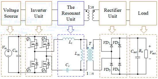
Figure 2.
The topology of the LLC resonant converter.
Moreover, the voltage gain curve is an intuitive reflection of the characteristics of the converter. Thereby, this paper adopts the first-order harmonic approximation (FHA) modeling approach to analysis the gain characteristics. In order to facilitate the analysis, the relevant physical quantities are defined as follows. The expressions of resonant frequency, f0, characteristic impedance, Zo, quality factor, Q, and equivalent resistance, Re, of the load resistance, Ro, are listed in Equations (1)–(2). The voltage gain curves of the LLC resonant converter with various loads are depicted in Figure 3. Here, the voltage gain of the LLC resonant converter, VgainLLC, is the ratio of the output voltage, Vout, and the input voltage, Vin. The ratio of the switching frequency, fs, to the resonant frequency, f0, is defined as the normalized frequency, fn. In this case, the value of Lr comprises of the leakage inductor of transformer T, thus the influence of the leakage inductor is not elaborated here. As can be seen in Figure 3, the LLC resonant converter consists of a frequency selective network. In other words, it could be considered as a bandpass filter. Voltage gain curves decrease along with increasing loads. Besides, the voltage gain at the resonant frequency, f0, is constant regardless of load changes. That is because the LLC resonant tank impedance is zero at f0, so the energy can be delivered to the load efficiently. However, when the switching frequency, fs, is larger than f0, the voltage gain is flat. This situation will bring about two effects. At first, the voltage regulation capacity of this converter is limited. That is to say, the very wide bandwidth, namely, poor frequency selectivity, the switching frequency needs to increase to a relatively high level to realize the voltage regulation. Secondly, over-current protection remains unresolved. As stated in [], during the start-up process, it is necessary to limit the inrush current. Additionally, in the condition of the short circuit or overload, the current stress of components should also be restricted. Thereby, the impedance of the converter is supposed to increase as much as the switching frequency.
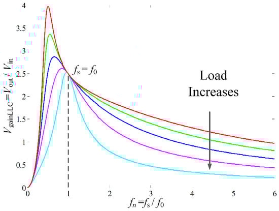
Figure 3.
DC voltage gain curves of an LLC resonant converter.
Based on the above analysis, the mentioned problems can be effectively solved by moving the switching frequency away from the resonant frequency. However, the increase in switching frequency will also bring in two more issues. For one thing, the increment of the switching loss will deteriorate the conversion efficiency. At high switching frequencies, requirements for devices are also improved accordingly. For another, a highly unbalanced stress of the magnetic components occurs, therefore increasing the difficulty in designing the magnetic elements. Consequently, this paper considers the addition of additional resonant elements to improve the voltage gain of the LLC, especially the segment which is above the resonant frequency.
2.2. Notch Filter
The notch filter is a kind of special resonant unit; the equivalent structure and the DC voltage gain are provided in Figure 4. It consists of an inductor, L, and a capacitor, C, in parallel. The expressions of equivalent impedance, Znotch, and the resonant zero frequency, fzero, are shown as follows. When the switching frequency, fs, operates at fzero, the resonant impedance is infinitely high, and the whole energy will be blocked in this unit. In other words, the notch filter can be considered as a band stop filter.
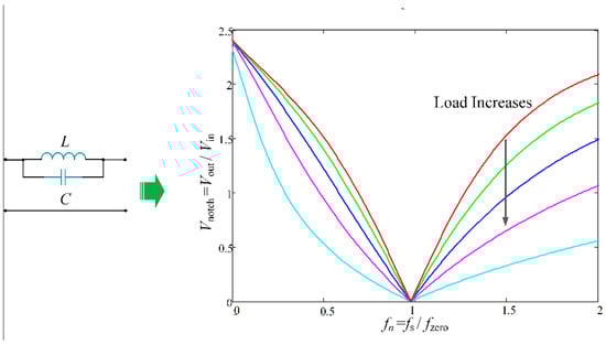
Figure 4.
The topology and DC voltage gain curves of the notch filter.
As seen, Vnotch is the DC voltage gain and fn is the normalized frequency, which is the ratio of fs to fzero. As seen, an additional resonant zero point (RZP) is introduced by its own structure. A constant zero voltage gain will be ensured at fzero. That is, the output port can be thought of as ‘totally disconnected’ from the input port. As a consequence, when the over-current occurs, the converter can work at RZP to effectively limit the current value, and thus, good over-current protection can be achieved.
2.3. LCCL Resonant Converter
Based on the above analysis, the LLC can be understood as a bandpass filter, while a notch filter can be regarded as a band stop filter. Combing the advantages of the above two, a four-element resonant converter LCCL can be obtained []. The basic topology is depicted in Figure 5. In comparison with LLC, LCCL owns an additional parallel resonant capacitor, Cp. So, it could perform the characteristics of the LLC and notch filter at the same time. Here, the notch filter section consists of Lr, Cp, and Cr. The bandpass filter section is created by Lr and Cp. Similar to the LLC resonant converter, the impact of the leakage inductor has been taken into account. There are two resonant frequencies, f01 and f02, and the corresponding definitions are listed in Equations (5) and (6), respectively [].
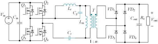
Figure 5.
The topology of the LCCL resonant converter.
The DC voltage gain curves of this converter under different loads are plotted in Figure 6. Its voltage gain is labelled as VgainLCCL; fn represents the ratio of fs to f01. As seen, VgainLCCL is maintained constant at frequency f01 and f02. Besides these frequency points, the gain curves have shown a downward trend with the increasing loads. In general, the gain curves changes rapidly within the frequency range from f01 to f02. Similar to the notch filter, f02 is the RZP, where the voltage gain is constantly zero in spite of load variation. Consequently, if the overload or even short circuit condition happens, the converter could work at this special point to restrict a sudden increase current. More importantly, the voltage gain range is broadened.
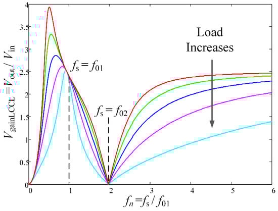
Figure 6.
DC voltage gain curves of the LCCL resonant converter.
2.4. The Proposed Structure Reconfigurable Resonant Converter
In light of the merits and the structural similarity of the LLC and LCCL, a two-mode structure-reconfigurable resonant converter is proposed in this paper. The equivalent topology of the proposed converter is shown in Figure 7. Here, Qa is an auxiliary switch, which is formed by a pair of MOSFETs (Metal-Oxide-Semiconductor Field-Effect Transistors) in series. It is adopted to change the equivalent circuit of the resonant unit.
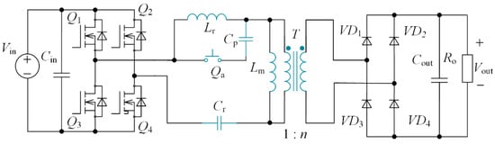
Figure 7.
The topology of the proposed converter.
To enhance the readability, the detailed performance analysis and parameter design process of the proposed converter are presented in the next chapter.
3. Topology Analysis and Parameter Design
On the basis of the above discussion, the proposed converter is a two-mode topology morphing converter. By controlling the adopted auxiliary switch, the structure of the resonant tank is adjustable. Specifically, when the auxiliary switch, Qa, is turned off, the proposed converter is acted as the LLC converter. Once the Qa is turned on, the resonant capacitor, Cp, participates in the resonance. In this case, the converter operates in LCCL mode. The corresponding structures under different modes are given in Figure 8.
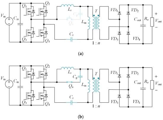
Figure 8.
Two different working modes of the proposed converter: (a) LLC mode; (b) LCCL mode.
In an effort to better understand the proposed converter, the performances of the LLC converter and LCCL converter are compared and discussed below.
3.1. The Comparison of Voltage Gain Characteristics
As stated in the previous section, these two converters illustrate very different features in terms of the voltage gain range.
For the gain issue, the LCCL converter possesses a wider voltage gain range. As seen in Figure 6, due to the adoption of RZP, the gain curves of LCCL becomes relatively sharp, thus broadening the low-value gain range to zero. When the input voltage changes rapidly, the LCCL circuit is capable of adjusting the voltage gain value within a narrow frequency range. In other words, a large promotion of the switching frequency can be avoided. Comparatively speaking, the LLC circuit does not have an RZP, so its voltage gain curves become gentle. Consequently, its voltage regulation is limited, especially the areas where the switching frequency is higher than the resonant frequency.
In consequence, the introduction of RZP obviously strengthens the competitiveness of the LCCL converter. Simply from the gain range aspect, the performances of the LCCL is better than the LLC.
3.2. The Comparison of Efficiency Characteristics
The efficiency factor is another important indicator that must be taken care of. Since the proposed converter has two working modes, the selection of the switching point is critical. To optimize the efficiency within the entire gain range, a comparison of efficiency is conducted in this section.
The efficiency comparison under the rated condition is discussed at first. Through the comparison of Figure 3 and Figure 6, both the LLC and LCCL will deliver high order harmonics at the rated point (resonant frequency point). As shown in Figure 6, with various loads, the voltage gain values of the LCCL are at a high level within a higher frequency range. The gain curves are almost parallel with each other. While for LLC, high gain values can only be reached near the operating frequency. In the higher frequency range, the gain value of the LLC is far smaller than that in the LCCL. These phenomena can be explained mathematically as follows.
For ease of analysis, the relevant physical quantities are defined as follows. N is defined as the Nth-order harmonics. Moreover, the frequency and angular frequency of the corresponding Nth-order components can be expressed as N f0 and N ω. Further combing the FHA modeling method discussed in [], the voltage gain of the LLC converter of Nth-order can be obtained as Equation (7). Herein, VReLLCn and VImLLCn denote the real and imaginary part of VLLCn:
A similar method is adopted for analyzing the LCCL converter. The high-order harmonics are analyzed as Equation (7), and the corresponding Nth-order components of the voltage gain of LCCL VLCCLn can be deduced as:
VReLCCLn and VImLCCLn represent the real part and imaginary part of VLCCLn. Since VReLLCn, VImLLCn, VReLCCLn, and VImLCCLn do not equal to zero in this case, that is, high-order harmonic power will be delivered in the resonant unit. Both the LLC and LCCL will transmit these harmonics at the rating point, and the proportions of the high-order components possess are not identical. A higher gain value within a higher frequency range means the larger proportion of high order harmonics. Generally, the larger the shares of high-order harmonics take up, the larger the circulating power is, and the smaller the efficient power is. Thus, from the aspect of efficiency optimization, exorbitant high order harmonics should be avoided in the resonant unit as far as possible. Thereby, it can be expected that with the same power and voltage level, the rating efficiency of LLC will have an edge over LCCL.
While when the switching frequency is higher than the resonant frequency, the efficiency circumstances of these two converters are quite different. As stated in [], the LLC converter loses the zero-current switch (ZCS) characteristic under this condition. The turn-off current also increases. Correspondingly, the turn-off losses increase sharply. With the increase of the switching frequency, the extra high-frequency losses are inevitably introduced. Besides, in order to guarantee a wide voltage gain range, the switching frequency should be far away from the resonant frequency in LLC mode. Whereas, in the same gain value, the variation of the frequency range of LCCL is relatively narrow. In this case, the operating frequency of LCCL is lower than that of LLC. It can be concluded that working in the LCCL state could successfully avoid the losses caused by a high frequency.
In summary, both converters possess their own merits but also suffer from some issues. To further synthesize the advantages of the above two, the converter mentioned in this paper can be formed. Taking the efficiency and voltage gain respects into consideration, the proposed converter operates in different modes under various conditions. In particular, the proposed converter will act as an LLC converter near the rating condition, which is to maintain a high efficiency. While when the input voltage is high, is works under LCCL mode to further extend the voltage gain range and acquire good overcurrent protection. The proposed converter is such a two-mode structure-reconfigurable converter.
3.3. The Parameter Selection Progress of the Proposed Converter
According to the above analysis, the converter first works in LLC mode. Hereby, the parameter design should meet the requirements of the LLC converter in the first place. In general, the rated parameters are preset as follows. The nominal input voltage, Vin, and output voltage, Vout, are 160 and 400 V, and the rated switching frequency, fr, is set as 100 kHz. The literature [,] has discussed several detailed parameter design methodology of LLC resonant converters. Accordingly, restricted by the length of this paper, it will not be repeatedly given. By consideration of the preconditions, the determined parameters are listed as follows: Cr = 79 nF, Lr = 32 μH, Lm = 128 μH, n = 2.5.
Until now, only the parallel resonant capacitor, Cp, in LCCL mode is undecided. From Equation (6), it is clearly seen that the position of f02 is directly related to the value of Cp. Accordingly, through the appropriate selection the RZP, Cp can be derived. In general, the placement of f02 should not be too far or too close to f01. On one hand, if f02 is far away from f01, the voltage gain curves keep a gentle trend. The voltage regulation capacity has not been fully improved within the frequency range from f01 to f02. On the other hand, if f02 is set very close to f01, the notch filter section will affect the nominal resonant frequency. In other words, it will trap energy, then energy will circulate in the notch unit. According to Fourier analysis, the input voltage of the resonant tank can be decomposed into a series of square waveforms. The corresponding voltage excitation only includes odd harmonics. Then, f02 should be designed at even times of f01. Through full consideration of the above factors, f02 is set at 200 kHz as a compromise. Correspondingly, Cp can be calculated as 20 nF here. The corresponding design flow chart is illustrated in Figure 9.
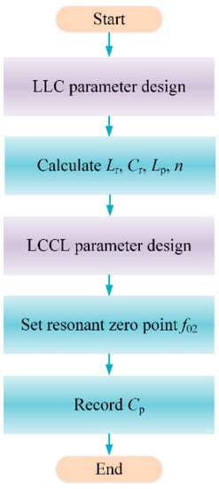
Figure 9.
The parameter design process.
At last, based on the mentioned parameter selection progress, all the parameters of the proposed converter can be obtained. Owing to the high similarity in structure, shared parameters Lr, Cr, Lm, and n are used by LLC and LCCL at the same time. Consequently, the proposed method could satisfy the operational requirements of both working modes.
In summary, the proposed converter operates in LLC mode at the rated condition, then steps into LCCL mode with the promotion of the input voltage. Based on the above analysis, the efficiency curve of the LLC is supposed to be above that of the LCCL and the gain is near the rated gain; whereas, the latter will be higher along with the increase in the input voltage and the gain is small. Consequently, there is an efficiency coincidence point between these two converters. Since the proposed converter is a two-mode converter, it is necessary to determine the switching point for the sake of excellent performance. Due to the expanded voltage gain range by topology-morphing, the efficiency issue is the remaining factor. Then, the efficiency intersection point is selected as the switching point for promoting the conversion efficiency. Hence, the loss issues must be estimated in the next step. The detailed loss analysis will be discussed in Section 4 of this paper.
4. Loss Analysis
To accurately locate the switching point, the loss calculation at different frequencies is conducted to estimate the efficiency. For the resonant DC-DC converter, five main parts of total power losses are considered. They include transformer losses, switch losses, diode losses, capacitor losses, and inductor losses in all. The detailed loss calculation is given below.
4.1. Transformer Losses
For a transformer, the main losses consist of two parts, conduction loss (copper loss) and magnetic loss (core loss).
The conduction loss is contributed to the current flowing through the primary-side and secondary-side windings of the transformer. Taking the primary-side of transformer T as an example, PT-con-pri is derived at first. Herein, RT-pri refers to the primary-side DC equivalent resistance. The expression is given in Equation (9). Moreover, ρCu is the electric resistivity of the copper wire, and SCu is the equivalent sectional area of the wires. lT is the length of the conductor:
Under the high-frequency circumstances, the skin effect makes the conductive currents closer to the surfaces of the conductors. Accordingly, the value of the AC resistance, RT-pri-ac, is higher than RT-pri. Thereby, based on Dowell’s equation stated in [], the correction coefficient, KT-ad, of AC conduction resistance can be expressed as:
where nlay represents the layers of the primary-side windings of T, MT is the intermediate variable given in Equation (11) []. Moreover, δn and dwire refer to the skin depth and the diameter of the copper wire, respectively. The corresponding expressions are given below:
In Equation (12), fs is the switching frequency and μ0 is the vacuum permeability.
In consequence, the primary-side conduction loss, PT-con-pri, can be calculated as Equation (13). I1(n) is the root mean square (RMS) value of the nth primary-side resonant current. In this example, only the first harmonic is taken into account, while other higher order components (n ≥ 3) are neglected due to the small proportion:
Similarly, the secondary-side conduction loss, PT-con-sec, is derived as follows. Herein, RT-sec represents the equivalent DC resistance, I1-sec(n) is the current flowing through secondary-side windings of transformer T. The AC-to-DC resistance ratio is denoted as KT-ad-sec. Then, the secondary side conduction loss, PT-con-sec, can be obtained:
As for magnetic loss, we can use the Steinmetz equation to estimate it. The flux swing, ΔBT, in a working period is given in Equation (15):
where VT is the primary-side voltage of T, Acore is the equivalent sectional area of the magnetic core. ts is the switching period. NTpri represents the number of primary-side windings.
So that, the magnetic loss, PT-mag, can be calculated in Equation (16):
Moreover, k, αcore, and βcore are Steinmetz coefficients, and Vcore refers to the volume of the magnetic core. The mentioned parameters are provided by the manufacturer [].
To sum up, the total transformer loss, PT, is expressed as:
4.2. Power Switch Losses
The MOSFET switches of the proposed converter include the switches, Q1–Q4, in the inverter unit and the auxiliary switch, Qa, used in the topology morphing process. The switch losses are composed of the switching loss, the driving loss, and the conduction loss. As for Qa, only the conduction loss is considered. In this section, taking Q1 as an example to describe the loss calculation process, the loss of Qa can be obtained similarly.
Switching loss is made up of the turn-on and turn-off losses. Since the proposed converter works in the ZVS state, the turn-on loss is restrained greatly. Accordingly, this part of loss can be ignored. Only the turn-off loss is considered here. The expression of switching loss, Pswi, is listed as follows:
In Equation (18), Iturnoff is the turn-off current of the power switch and can be gained mathematically. Vin is the input voltage. Besides, QGD, QGS refers to the storage charges between the gain and drain, the gate and source, respectively. Vpl and Vth are the miller plane voltage and the gate threshold voltage. RG and Rs1 denote the equivalent gate impedance and the serial source equivalent impedance, respectively. These mentioned parameters can be acquired in the relevant datasheet.
Driving loss, Pdri, is generated by the driving process. The corresponding equation is shown in Equation (19). Herein, VGD is the driving voltage:
Conduction loss, Pcon, is the power loss produced by the on-resistance, Rsw, of Q1 when the resonant current, I1(n), passes through it. The equation is deduced as:
From Equations (18)–(20), the switch loss, PQ1, of a single power switch, Q1, can be harvested:
4.3. Diode Losses
The calculation of diode losses is similar to that of switch losses. Because the diodes, VD1–VD4, are uncontrolled devices, only the switching loss and conduction loss are considered here.
Similar with the MOSFETs, the diodes have realized the ZCS turn-off switching, and thus, only the turn-on loss is estimated. For VD1, its switching loss, Pswi-VD1, is derived in Equation (22). Here, Ion-VD1 is the turn-on current of VD1, VVD1 is the reverse bias voltage, and tr is the turn-on period:
Furthermore, the conduction loss, Pcon-VD1, is described below. Within the conduction time, tcon-VD1, the RMS current, Icon-VD1, flows through VD1 and produces power loss, Pcon-VD1, on the forward-bias voltage, VF. Then, Pcon-VD1 can be calculated as:
As a result, the single diode losses, PVD1, is:
4.4. Capacitor Losses
The resonant capacitors and filter capacitors are both adopted in the proposed converter. So, each kind of capacitor is calculated separately.
4.4.1. Resonant Capacitor Losses
The resonant capacitors are connected in series in the power path, which takes on a relatively high current. In an effort to achieve high efficiency, the MKP metalized polypropylene film capacitors are employed because of its low dissipation factor, DF. In LLC mode, only the serial resonant capacitor, Cr, takes part in resonance. While in LCCL mode, both Cr and the parallel resonant capacitor, Cp, are involved in the resonant unit. Herein, we only take Cr for instance.
The serial equivalent resistance, RCr, is defined in Equation (25). Here, aDF and bDF are the fitting parameters based on the fitting curves:
Consequently, the capacitor loss, PCr, of Cr can be calculated as:
4.4.2. Filter Capacitor Losses
Filter capacitors are employed for the maintenance of the DC voltage stability of the proposed converter in both the input port and output port. Their respective losses are derived in Equations (29) and (30). Here, RCin and RCout denote the equivalent resistance of the input port and output port, respectively. nCin and nCout are the numbers of capacitors used for input and output. Irip-in and Irip-out refer to the corresponding ripple currents. Their value can be obtained by summing the frequency harmonic components from the fundamental frequency to the frequency of the 32nd harmonics. The expression is given in Equation (28):
4.5. Inductor Losses
The inductor losses’ estimation approach of the inductor, Lr, is basically the same as that of the transformer losses. They also include two main parts, conduction loss, PLrcon, and magnetic loss, PLrmag. More specifically, PLrcon can be attained through Equations (9)–(13), so is no longer elaborated here. Different from transformer T, there is no secondary-side conduction loss for inductor Lr and the flux swing, ΔBLr, is estimated in Equation (31):
ILr-max is the peak current passing through Lr, NLr is the winding turns, and Acore is the effective cross-sectional area of the inductor core.
On this basis, the inductor losses, PLr, can be harvested as Equation (32):
To summarize, the efficiency values of LLC and LCCL at different frequencies can be calculated separately, then the corresponding efficiency curves can be drawn. The detailed loss distribution at the voltage gain, Vgain, of 2.5 and 2 are shown in Figure 10. As seen, at the rated condition (Vgain equals 2.5), the efficiency of LLC is better than LCCL. That is because there are higher high-order harmonics in the LCCL converter. When Vgain equals 2, the efficiency of these two modes is nearly same. Compared with LLC mode, the conduction losses of the auxiliary switch and the additional loss caused by high-order harmonics are inevitable in LCCL mode. However, the high-frequency losses are restricted to a certain extent. So, at this point, the efficiency of these two modes is balanced. Through the theoretical calculation, the intersection of the two efficiency curves is the equal efficiency point, and its value is about 2. Then, this point is chosen as the switching point to further optimize performances.
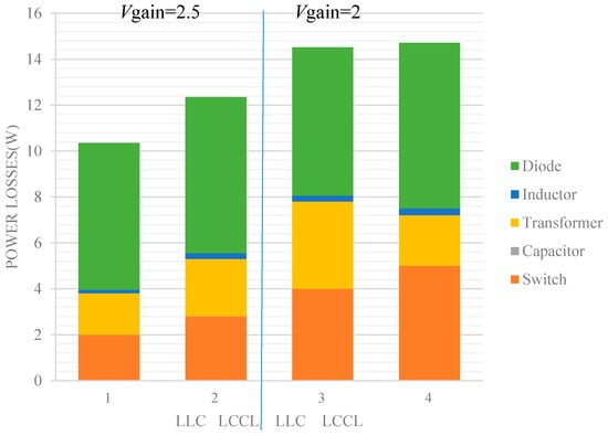
Figure 10.
The calculated efficiency comparison of the LLC and LCCL under different gain conditions.
To validate the effectiveness of the theoretical analysis, the detailed experimental results, as well as the comparison between the calculated efficiency and the measured efficiency are elaborated in the next chapter.
5. Experimental Results
A 500 W experimental prototype for small-scale wind generation systems was built and is shown in Figure 11. The involved components and the specifications are listed in Table 1. Here, the DC power supply (Agilent Technologies N8762A) was used to simulate the wind power generation unit, and the DC resistance acted as the output load. Then, the experimental waveforms were observed with an oscilloscope (Agilent Technologies DSO-X 3034A). The digital controller is Texas Instruments TMS320F28379D.
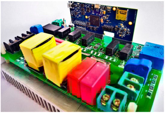
Figure 11.
Photograph of the prototype built in the laboratory.

Table 1.
Main components of the proposed converter.
Through the calculation results, the point, with the voltage gain of 2, was chosen as the switching point. Therefore, the compound DC voltage gain curves can be drawn in Figure 12. Here, mode I and II separately denote the LLC mode and LCCL mode for convenience. In this case, the recombination voltage gain, Vgain, and the normalized frequency, fn, are noted as well. The compound gain curve, as indicated by the arrow directions, is composed of two sections, and each part is a certain counterpart of these two modes. That is, the converter first operates in mode I, and once the optimal switching point is reached, it steps into mode II subsequently. Moreover, five special points (point①, ①’, ②, ③, ④) are signed in this figure. Next, the verification of these five points is discussed in detail.
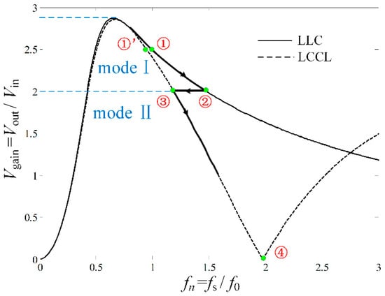
Figure 12.
The expected gain curve of the proposed converter.
Point ① is the rated operating point in mode I and the corresponding frequency is 100 kHz. Figure 13 shows the resulting waveforms at this point. Here, Vgs is the driving signal, VQ1 and iQ1 represent the voltage and current of Q1. Similarly, VVD1 and iVD1 are the matching electrical quantities of VD1. VCr is the voltage across the resonant capacitor, Cr. Under this case, the input voltage is 160 V and the output voltage is 400 V. The calculated voltage gain is 2.49, which matches well with the theoretical design. As shown in Figure 13a, iQ1 lags behind an angle of VQ1, it means that the power switches achieve the desirable ZVS turn-on. It is demonstrated by the antiparallel diode turning on earlier than the MOSFET itself. In this case, the turn-off current is small and approximate to zero, which can be considered that the power switches achieve the quasi-ZCS turn-off feature. Moreover, the desirable ZCS soft switching of secondary-side diodes is also required. In such a way, the measured efficiency is 97.2%. It further confirms that the proposed converter could maintain a high conversion efficiency at the nominal condition.
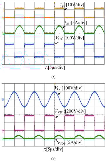
Figure 13.
Experimental waveforms at rated point. (a) Waveforms of Q1. (b) Waveforms of VD1 and Cr.
Figure 14 provides the resulting waveforms at point ①’. As seen in Figure 12, point ①’ in mode II owns the same gain point as point ①, and its working frequency is 92 kHz. In this case, the input voltage is still maintained at 160 V, and the measured output voltage is 402.2 V. The corresponding voltage gain value is 2.51. The electrical quantities in this figure are identical to that in Figure 13. Compared with Figure 13, both currents of the primary and the secondary sides contain a large proportion of high-order harmonics. Generally, these harmonics increase losses and deteriorate the conversion efficiency as well, and the efficiency of this point is measured as 96.7%. Consequently, the proposed converter will operate at point ① instead of point ①’ to guarantee a high conversion efficiency.
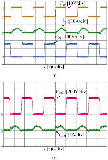
Figure 14.
Experimental waveforms at point ①’ in mode II. (a) Waveforms of Q1. (b) Waveforms of VD1.
According to Figure 12, point ② is the switching point operating in mode I. The corresponding voltage gain equals 2 at this point. The relevant experimental waveforms are shown in Figure 15. In this case, the input voltage is 200 V, and the output voltage is 398.7 V. As can be seen in this figure, the current, iQ1, still lags behind the voltage, VQ1, demonstrating the power switch could achieve preferable ZVS soft switching. However, the ZCS characteristics of the LLC are lost in this case. During the turn-off process, the shutdown current becomes large. Accordingly, this will further increase the switching loss and decrease the efficiency. The efficiency is measured as 96.3% at this point.
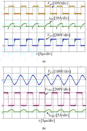
Figure 15.
Experimental waveforms at point ② in mode I. (a) Waveforms of Q1. (b) Waveforms of VD1 and Cr.
To optimize the performances of the proposed converter, as the input voltage rises, the auxiliary switch, Qa, is turned on and then the converter steps into mode II. The resulting experimental waveforms at point ③ are illustrated in Figure 16. Specifically, the input voltage is still kept at 200 V, and the relevant output voltage value is 402.3 V, which is in good agreement with that at point ②. The stability of the value of the output voltage further indicates the feasibility of the topology morphing. The resulting waveforms, given in this figure, show that high-order harmonics exist in both the primary-side and secondary-side. However, at this point, the working frequency is relatively low, avoiding the high-frequency magnetic losses caused by an excessive operating frequency accordingly. Thus, it yields an efficiency of 96.1%. It matches well with the efficiency at point ②. Based on the above analysis, both the efficiency and the output voltage keep a smooth and steady transition, so that the preferable performance of the converter can be ensured.
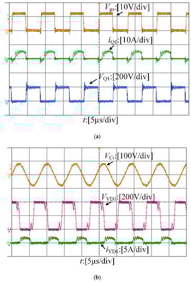
Figure 16.
Experimental waveforms at point ③ in mode II. (a) Waveforms of Q1. (b) Waveforms of VD1 and Cr.
Afterwards, the working state of the proposed converter operates in mode II all the time. The experimental waveforms at point ④ are presented in Figure 17. On the basis of the above discussion, the RFP is the special frequency point introduced by the topology itself. Seen from this figure, when the input voltage is 400 V, the output voltage is only around 3 V. Additionally, the current is restrained to a relatively small value. It indicates that the input power is absorbed by the topology totally. Hence, working at this point could obtain good over-current protection. Compared to other converters, there is no need for extra protection circuits. In other words, the reliability can be enhanced.
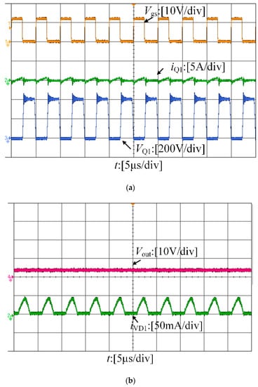
Figure 17.
Experimental waveforms at RZP. (a) Waveforms of Q1. (b) Waveforms of VD1 and output voltage, Vout.
Then, the specific efficiency was measured by a power analyzer (YOKOGAWA WT3000) and is plotted in Figure 18. There are four efficiency curves in all, here mode I-Cal, mode I-Mea curves are the calculated and measured efficiency curves in mode I, and the mode II-Cal, mode II-Mea are the corresponding curves in mode II. Seen from this figure, the calculated value is higher than the measured value throughout. The voltage gain of the intersection points of the calculated efficiency curves and measured efficiency curves are all close to 2. The deviation is within an acceptable range. Through the comparison, the correctness of the stated loss analysis method can be effectively verified. Then, the efficiency of the proposed converter is no less than that of any mode. In such a way, the converter maintains a relatively high-efficiency value within the entire gain range (above 92%). Additionally, the maximum efficiency of 97.2% is obtained at the nominal condition.
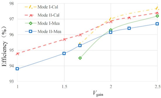
Figure 18.
Efficiency curves of different modes at the rated power.
The specific control block diagram of the proposed converter is shown in Figure 19. As seen, it consists of two main parts, closed-loop control and logical selection. For the former, the pulse frequency modulation control is used by changing the switching frequency, fs, to achieve the output voltage constant. Besides, the proposed converter is a two-mode topology-morphing converter, the mode transition is realized by the logical selection, and is based on the change of the input voltage. The detailed control processes are discussed below.
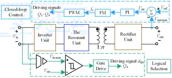
Figure 19.
Control strategy scheme of the proposed converter.
For the closed-loop control, the measured signal, Vout-mea, is firstly acquired by a resistance voltage divider, optical isolation amplifier (ACPL-C87A), and operational amplifiers. Then, the voltage error, Verr (Verr = Vref − Vout-mea), the difference between the reference voltage, Vref, and the Vout-mea, is sent to the proportional integral (PI) controller. Afterwards, the adjusting result, fs, is obtained by the frequency modulator (FM). In the end, fs is transmitted to the pulse width modulator (PWM) to generate the driving signals for Q1–Q4.
Meanwhile, the input voltage is detected to determine whether the mode transformation is required. The measured input voltage, Vin-mea, which is acquired by a voltage sensor (Voltage Transducer LV 25-P), is compared with the preset voltage, Vset, to control the on/off state of the auxiliary switch, Qa. Here, dQa is the driving signal of the auxiliary switch, Qa. At first, the input voltage is in a relatively low value, and the dQa has not been triggered. Thus, the auxiliary switch, Qa, is not involved in resonance and the corresponding working mode is mode I. Then, when the input voltage reaches about Vset, the optimal switching point is achieved. In this case, dQa is set high to make Qa conduct, and correspondingly the converter steps into mode II. Afterwards, the working mode is still in mode II regardless of the increase of the input voltage. Throughout the mode transformation process, the variable frequency control has been working to maintain the stability of the output voltage.
Furthermore, to test the effectiveness of the topology morphing process, the mode transition was carried out with the abovementioned control method and is presented in Figure 20. Here, iCr is the current passing through Cr, namely, the resonant current. As seen, the experimental results are in good agreement with the control strategy, thus the reliability of the proposed converter is demonstrated as well.
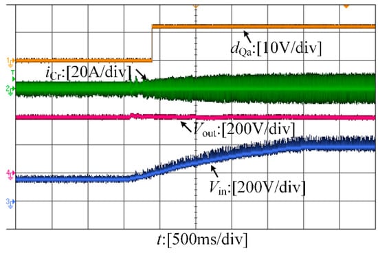
Figure 20.
Experimental waveforms of mode transition.
Moreover, experiments at the 50% rated power (250 W) and 20% rated power (100 W) were conducted for comparative analysis. The relevant efficiency curves are shown in Figure 21. The corresponding physical quantities are consistent with Figure 18.
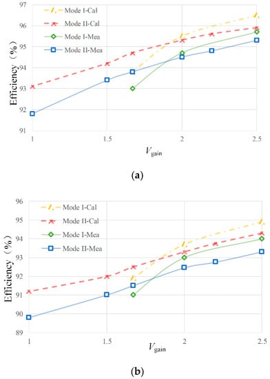
Figure 21.
Efficiency curves of different modes (a) at 250 (b) at 100 W.
From this figure, it can be clearly seen that the calculated efficiency is higher than the measured efficiency throughout, but the deviations are generally around 1%. Generally, along with the power level decreases, the efficiency deteriorates, and the efficiency intersection point moves slightly to the left. The reasons are listed as follows. For one thing, mode II is used to broaden the voltage gain range within a narrow frequency range, but at the same time, high-order harmonics are inevitably introduced. This phenomenon is particularly serious at light loads. For another, relatively speaking, the lower switching frequency in mode II is no longer more dominant than that in mode I. In this case, the losses introduced by high-order harmonics in mode II are larger than the losses caused by a high frequency in mode I. Thus, the efficiency of mode II decreases rapidly; that is, the efficiency crossing point of two modes shifts to the left. Even so, the converter still maintains a relatively high conversion efficiency throughout the gain range.
As stated above, the proposed converter could not only obtain high efficiency but also acquire a wide voltage gain range. The experimental results are verified effectively and reliability as well.
6. Conclusions
In this paper, a structure-reconfigurable soft-switching resonant DC-DC converter was proposed. By the introduction of an auxiliary switch, it changed the equivalent structure to satisfy various conditions. It has two operating modes in total, namely LLC and LCCL. At the rated condition, the converter works in LLC mode to maintain a high efficiency. With the rise of the input voltage, it enters LCCL mode to acquire a wide voltage gain range. The structure is relatively simple and the control strategy is easy to implement as well. Meanwhile, the resonant zero-point can be introduced by the topology itself. The good over-current protection is guaranteed without an extra additional circuit. Moreover, loss analysis was conducted to locate the optimal switching point. At last, a 500 W prototype was built in the laboratory to demonstrate the effectiveness and rationality further. The measured peak efficiency was 97.2%. The output voltage remained constant at 400 V even when the input voltage increased from 160 to 400 V. These good performances make it a good candidate for small-scale grid-connected wind generation systems.
Author Contributions
X.H., K.X., and R.L. designed the main parts of the study, including the circuit design, switching point selection research, and experiment. X.C., Z.L., and H.Y. helped in the hardware design, experiment and some theoretical analysis.
Funding
This research was funded by the National Key R&D Program of China (Grant number: 2018YFB0904700).
Conflicts of Interest
The authors declare no conflict of interest.
Abbreviations
The following abbreviations are used in this manuscript:
| DC-DC | direct current – direct current |
| LLC | inductor-inductor-capacitor |
| LCCL | inductor-capacitor-capacitor-inductor |
| SRC | series resonant converter |
| PRC | parallel resonant converter |
| ZVS | zero voltage switch |
| ZCS | zero current switch |
| ICN | impedance control network |
| DSBS LLC | LLC converter with dual-bridge and two split resonant branches |
| FHA | first-order harmonic approximation |
| RZP | resonant zero point |
| MOSFETs | Metal-Oxide-Semiconductor Field-Effect Transistors |
| RMS | root mean square |
| PI | proportional integral |
| FM | frequency modulator |
| PWM | pulse width modulator |
References
- Guan, Y.; Wang, Y.; Wang, W.; Xu, D. Analysis and design of a 1-MHz single-switch DC-DC converter with small winding resistance. IEEE Trans. Ind. Electron. 2018, 65, 7805–7816. [Google Scholar] [CrossRef]
- Sarkar, M.; Altin, M.; Sorensen, P.E.; Hansen, A.D. Reactive power capability model of wind power plant using aggregated wind power collection system. Energies 2019, 12, 1607. [Google Scholar] [CrossRef]
- Tomczewski, A.; Kasprzyk, L.; Nadolny, Z. Reduction of power production costs in a wind power plant-flywheel energy storage system arrangementd. Energies 2019, 12, 1942. [Google Scholar] [CrossRef]
- Huang, Y.; Yang, L.; Liu, S.; Wang, G. Multi-step wind speed forecasting based on ensemble empirical mode decomposition, long short term memory network and error correction strategy. Energies 2019, 12, 1822. [Google Scholar] [CrossRef]
- Wang, C.; Yang, L.; Wang, Y.; Meng, Z.; Li, W.; Han, F. Circuit Configuration and Control of a Grid-Tie Small-Scale Wind Generation System for Expanded Wind Speed Range. IEEE Trans. Power Electron. 2017, 32, 5227–5247. [Google Scholar] [CrossRef]
- Khouzani, A.S.; Dehkordi, B.M.; Kiyoumarsi, A.; Farhangqi, S. A Control Approach for Small-Scale PMSG-based WECS in the Whole Wind Speed Range. IEEE Trans. Power Electron. 2017, 32, 9117–9130. [Google Scholar]
- Chen, M.; Wang, Y.; Yang, L.; Han, F.; Hou, Y.; Yan, H. A variable-structure multi-resonant DC-DC converter with smooth switching. Energies 2018, 11, 2240. [Google Scholar] [CrossRef]
- Shafiei, A.; Dehkordi, B.M.; Farhangi, S.; Kiyoumarsi, A. Overall power control strategy for small-scale WECS incorporating flux weakening operation. IET Renew. Power Gener. 2016, 10, 1264–1277. [Google Scholar] [CrossRef]
- Xia, Y.Y.; Fletcher, J.E.; Finney, S.J.; Ahmed, K.H.; Williams, B.W. Torque ripple analysis and reduction for wind energy conversion system using uncontrolled rectifier and boost converter. IET Renew. Power Gener. 2011, 5, 377–386. [Google Scholar] [CrossRef]
- Steigerwald, R.L. A comparison of half-bridge resonant converter topologies. IEEE Trans. Power Electron. 1988, 3, 174–182. [Google Scholar] [CrossRef]
- Fang, X.; Hu, H.; John Shen, Z.; Batarseh, I. Operation mode analysis and peak gain approximation of the LLC resonant converter. IEEE Trans. Power Electron. 2012, 27, 1985–1995. [Google Scholar] [CrossRef]
- Fang, Z.; Cai, T.; Duan, S.; Chen, C. Optimal design methodology for LLC resonant converter in battery charging applications based on time-weighted average efficiency. IEEE Trans. Power Electron. 2015, 30, 5469–5483. [Google Scholar] [CrossRef]
- Kundu, U.; Yenduri, K.; Sensarma, P. Accurate ZVS analysis for magnetic design and efficiency improvement of full-bridge LLC resonant converter. IEEE Trans. Power Electron. 2017, 32, 1703–1706. [Google Scholar] [CrossRef]
- Lee, J.; Kim, J.K.; Kim, J.H.; Baek, J.; Moon, G.W. A high-efficiency PFM half-bridge converter utilizing a half-bridge LLC converter under light load conditions. IEEE Trans. Power Electron. 2015, 30, 4931–4942. [Google Scholar] [CrossRef]
- Kim, C.E.; Baek, J.I.; Lee, J.B. High-efficiency single-stage LLC resonant converter for wide-input-voltage range. IEEE Trans. Power Electron. 2018, 33, 7832–7840. [Google Scholar] [CrossRef]
- Lu, J.; Perreault, D.J.; Otten, D.M.; Afridi, K.K. Impedance control network resonant DC-DC converter for wide range high efficiency operation. IEEE Trans. Power Electron. 2016, 31, 5040–5056. [Google Scholar]
- Guan, Y.; Wang, Y.; Cecati, C.; Wang, W.; Xu, D. Analysis of frequency characteristics of the half-bridge CLCL converter and derivative topologies. IEEE Trans. Power Electron. 2018, 65, 7741–7752. [Google Scholar] [CrossRef]
- Wu, H.; Jin, X.; Hu, H.; Xing, Y. Multi-element resonant converters with a notch filter on secondary side. IEEE Trans. Power Electron. 2016, 31, 3999–4004. [Google Scholar] [CrossRef]
- Iqbal, S. Interleaved LLC resonant converter with integrated dual transformer for PV power systems. In Proceedings of the IET 8th International Conference on Power Electronics, Machines and Drives (PEMD), Glasgow, UK, 19–21 April 2016; pp. 1–6. [Google Scholar]
- Wang, H.; Chen, Y.; Fang, P.; Liu, Y.; Afsharian, J.; Yang, Z. An LLC converter family with auxiliary switch for hold-up mode operation. IEEE Trans. Power Electron. 2017, 32, 4291–4306. [Google Scholar] [CrossRef]
- Sun, W.; Xing, Y.; Wu, H.; Ding, J. Modified high-efficiency LLC converters with two split resonant branches for wide input-voltage range applications. IEEE Trans. Power Electron. 2018, 33, 7867–7879. [Google Scholar] [CrossRef]
- Hu, H.; Fang, X.; Chen, F.; Shen, Z.J.; Batarseh, I. A modified high efficiency LLC converter with two transformers for wide input-voltage range applications. IEEE Trans. Power Electron. 2013, 28, 1946–1960. [Google Scholar] [CrossRef]
- Yang, B.; Lee, F.C.; Concannon, M. Over current protection methods for LLC resonant converter. In Proceedings of the Eighteenth Annual IEEE Applied Power Electronics Conference and Exposition, Miami Beach, FL, USA, 9–13 February 2003; pp. 605–609. [Google Scholar]
- Fu, D.; Lee, F.C.; Liu, Y.; Xu, M. Novel multi-element resonant converters for front-end DC/DC converters. In Proceedings of the 2008 IEEE Power Electronics Specialists Conference, Rhodes, Greece, 15–19 June 2008; pp. 250–256. [Google Scholar]
- Simone, S.D.; Adragna, C.; Spini, C.; Gattacari, G. Design-oriented steady-state analysis of LLC resonant converters based on FHA. In Proceedings of the International Symposium on Power Electronics, Electrical Drives, Automation and Motion, Taormina, Italy, 23–26 May 2006; pp. 200–207. [Google Scholar]
- Chen, B.; Wang, P.; Wang, Y.; Li, W.; Han, F.; Zhang, S. Comparative analysis and optimization of power loss based on the isolated series/multi resonant three-port bidirectional DC-DC converter. Energies 2017, 10, 1565. [Google Scholar] [CrossRef]
- Ferreira, J.A. Improved analytical modeling of conductive loses in magnetic components. IEEE Trans. Power Electron. 1994, 9, 127–131. [Google Scholar] [CrossRef]
- Ferroxcube Application Note: Design of Planer Power Transformers. 2019. Available online: https://www. Ferroxcube.com (accessed on 30 May 2019).
© 2019 by the authors. Licensee MDPI, Basel, Switzerland. This article is an open access article distributed under the terms and conditions of the Creative Commons Attribution (CC BY) license (http://creativecommons.org/licenses/by/4.0/).