Abstract
The energy yield of a solar panel can be severely impacted by partial shading. Shade caused by nearby static objects can hardly be avoided in installations such as building-applied or building-integrated photovoltaics. Smart reconfigurable photovoltaics (PV) panels are able to change their intra-module configuration to reduce this impact: small substrings can be rewired to be connected in a more optimal configuration. To achieve this, a reconfiguration switch needs to be designed. In this paper a switch for the optimization of module power by reconfiguration of all strings (SOMBRA), a smart switch, is presented. SOMBRA is a fully integrated, low-ohmic switch, designed for currents up to 10 A. It is fully floating up to 50 V, while still being able to communicate with a central unit as an inter-integrated circuit (IC) slave. Two versions were realized, SOMBRA-LV10 for low voltages (LV) and a load current of 10 A, and SOMBRA-HV05 for high voltages (HV) and a load current of 5 A. Measurements proved these devices to be functional, measuring an on-resistance of 1.3 m for SOMBRA-LV10 and 7.3 m for SOMBRA-HV05. This paper will elaborate on the operation, design, and implementation of SOMRBA, as well as the first tests with a small reconfigurable PV module.
Keywords:
photovoltaic power; power loss; partial shading; power optimization; panel reconfiguration; smart switch PACS:
J0101
1. Introduction
In our continuous search for cleaner and greener energy, the use of solar energy is fairly obvious. Photovoltaic cells allow us to directly convert the power of the sun to electric power. Already in 1961, it was clear that the maximum efficiency of this energy conversion is limited. According to the calculations by Shockley and Queisser, this maximum efficiency for a single p-n junction is 33.7% [1], which can be reached using a perfect semiconductor with a bandgap of 1.34 eV. For now, the most economically viable material for solar cells is silicon (Si). With a bandgap of 1.12 eV, this efficiency is slightly lower. In fact, Richter et al. [2] did a more detailed analysis specifically for Si cells and came to the conclusion that the theoretical maximum efficiency was limited to 29.4%. In 2019, Green et al. [3] reported a record cell efficiency of 26.7% for a monocrystalline Si-cell. What this shows is that we are nearing the end of the steady improvement of Si-cell efficiency. On the other hand, the maximum reported Si module efficiency is reported to be 24.4% [3]. These efficiencies are measured under the global AM1.5 spectrum (1000 W/m) at a cell temperature of 25 C. In more realistic conditions, the average efficiency may drop down 20% or even lower, depending on the surrounding environment. Cell density within the module, wire resistance, etc. explain the difference between the record efficiency on the cell level and module level. In a real setting using commercial modules, the average efficiency is further lowered by mass production (not every panel has the record efficiency), suboptimal conditions, mismatches between cells within a module and between modules. Another important factor affecting this average efficiency is the presence of partial panel shading. This effect will not play a large role in solar plants, where this shading is minimized (although dynamic shading by clouds will still occur), but in residential settings such as installations on a roof (building applied photovoltaics (BAPV)) and building-integrated photovoltaics (BIPV), it may be the cause of significant energy loss.
As the cells within a module are typically placed in series, the output current is limited by the cell generating the lowest current. In a panel under partial shading conditions, not only the power of the shaded cells is lost, but the output power of the non-shaded cells is dramatically reduced [4]. The generated power not delivered to the load is dissipated within the panel itself, creating hot spots, which may cause permanent panel damage [5,6]. There are several ways to mitigate this problem. In commercial photovoltaics (PV) systems, bypass diodes are placed across a number of cells (typically 20 cells) to create a substring. When one or more of the cells within a substring are shaded, this substring can be bypassed. The cells within the substring will not contribute to the output power, but the cells in the other substrings can work at full capacity.
This approach has a couple of shortcomings. The bypass, albeit most likely a Schottky diode, will itself consume a few watts of power. This can be avoided by using a more intelligent implementation of the bypass diode: a low-ohmic switch with control logic to let it act as a bypass diode [7,8]. A second and more important shortcoming is the fact that when a substring is bypassed, any power that may be generated in this substring is completely lost. Parallel connections between the cells can be introduced to ensure that the output current will not be blocked when just a single cell is shaded. It has been shown that a totally cross-tied (TCT) configuration, where all the cells are connected in a mesh network, is optimal in terms of power output [9,10]. However, adjusting the traditional solar panel configuration to the TCT configuration is not so straightforward, and the possibly very high currents which may flow through some of those connections can be problematic. A third issue is that the introduction of a bypass diode reshapes the power versus voltage curve when the module is partially shaded, creating more than one (local) maximum power point (MPP) [11,12,13,14]. Since the position of the array’s MPP changes with the environmental conditions, several maximum power point tracking (MPPT) algorithms have been proposed in both past and recent literature [15]. Simple MPPT algorithms such as Open Circuit Voltage method are easy to implement, but lead to low MPPT efficiency (90%), more complex solutions (perturb and observe, artificial neural networks) get higher efficiencies, but require the sensing of current and voltage, and might meed expensive microprocessors. In any case, none of these solutions address the problems of the intra-module non-uniformities.
Baka et al. [16] propose a new approach. This innovative and flexible topology enables multiple run-time configurations, depending on the current operating conditions of the PV module. Substrings can be connected either in parallel or in series. High currents are avoided by locally boosting the voltage. Many design parameters have to be considered during the design process. The most suitable granularity level has to be explored by taking into consideration the increased manufacturing cost due to additional elements and the increased resistivity in the active path of the current. Dynamic elements (switches), local DC–DC converters and a supporting network have to be added to allow extraction of additional power during non-uniform conditions. The net power gain (including all losses due to the added components) of these PV modules is difficult to quantify, as it is entirely dependent on the specific shading scenarios. A basic assessment is made in [16,17], showing that even with low shade intensities significant power output gains (30%) can be achieved. Preliminary cost estimations indicate that such Smart PV Panel [18] might be made cost-effective [17,19] (see also Section 4).
We continue the work of Baka et al. [16] and take the first steps in creating a reconfigurable panel. In this paper, we focus on the design, implementation, and preliminary results of the reconfiguration switch, which we coined switch for the optimization of module power by reconfiguration of all strings or SOMBRA. As we’ll see in the following section, the reconfigurable panel requires a galvanically isolated, remotely addressable, high-current switch. While isolated gate drivers do exist [20,21], they are not remotely addressable and lack internal power management. Communication together with galvanic isolation can be introduced by using isolated inter-integrated circuits (IC) devices. The communication across the isolation can be inductive [22], opto-electronic [23,24] or capacitive [25]. However, these devices still need external power management, a control system managing the communication, and the switch driver. On top of that, these devices are generally not meant to be used in reversed polarity. With SOMBRA, we’re creating a single, fully integrated device, meeting all the requirements for this reconfigurable solar panel. In this paper, we will also explore a solution to cope with changing polarity.
2. Design and Implementation of the SOMBRA
2.1. Requirements
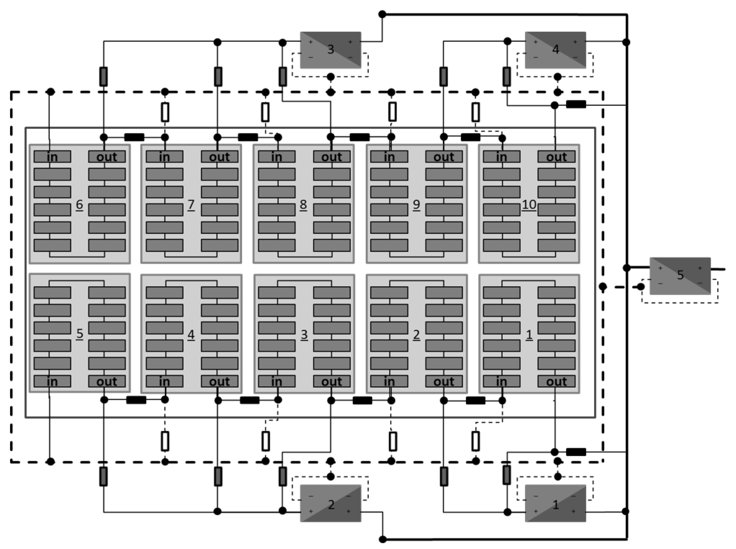
Before going into the details of the SOMBRA, it is good to first have a look at the reconfigurable topology. Figure 1 shows a slightly modified version of what is presented in [16]. The panel consists of either 60 standard cells (each producing around 0.6 V with 8 A current under standard lighting conditions) or 120 ‘half-cells’ (each producing 0.6 V with 4 A current). We opted to focus on the half-cells, as this increases the voltage and lowers the current, reducing the current losses in the system. These 120 cells are grouped in 10 substrings of 12 cells each. The series connection within such a substring is fixed and will not change between configurations. They determine the granularity of the system. These substrings are connected to each other through switches (horizontal black rectangles in Figure 1). Other switches (vertical white rectangles) connect certain points to the ground line (represented by the dashed line around the panel). Even other switches (vertical gray rectangles) connect certain points to the inputs of the local DC–DC converters (components 1–4, see below). The outputs of these converters and the input of the module converter (component 5, see below) are connected to the power line, represented by a full thick line. There are also (black) switches connecting this power line to some of the substrings.

Figure 1.
Schematic representation of the smart reconfigurable photovoltaics (PV) panel proposed by Baka et al. [16]. There are 10 substrings of 12 ‘half-cells’ each. On the outside, components 1–4 represent the local DC–DC converters. Component 5 represents the module level converter. The reconfiguration switches allow the different configurations.
Without paying attention to the other components, the reader can see that if all the black switches are active, the result is as follows: all the cells in the top half of the panel are connected in series, with the anode of the first cell connected to the power line (right side of the panel in Figure 1), and the cathode of the last cell connected to the ground line. This is identical to the cells in the bottom half of the panel. As this panel consists of half cells, there are now two large strings of 60 cells connected in parallel, resulting in an output voltage and current that is the same as a traditional panel. The power and ground lines are the input of a module-level converter (component 5) which can boost the voltage for either a grid connection or a module array.
The switches also allow configurations where the substrings are grouped and connected in parallel (e.g., by deactivating the black switches and activating the gray and white switches). Connecting all substrings in parallel is not advisable as this would generate very large currents (up to 40 A) resulting in very large losses in the power lines and module-level converter. Also, the output voltage would be that of a single substring (around 7 V) which is too low for standard module-level converters. In the proposed reconfigurable panel, a couple of substrings (2 or 3) are grouped together and their voltage is boosted by a small local converter (components 1–4). This not only decreases the current in the power line and module converter input but allows us to boost the voltage to a value that is optimal for this module converter.
With this information, we can determine the requirements for the reconfiguration switches. Obviously, the resistance of the switch should be as low as possible (a couple of ms). On the other hand, devices with a lower on-resistance need to be larger, which makes them more expensive. This is further discussed in Section 4. The maximum current the switch should be able to handle is limited to 5 A. The maximum blocking voltage is the maximum voltage generated by a single substring (). This is higher than the standard low voltage (LV) value, normally limited to 3.6 V, meaning we have to look at a high voltage (HV) chip technology. The devices in an HV technology are usually a lot larger than similar devices in an LV technology. To limit the overall cost, it is a good idea to also create an LV version, as not necessarily all switches will need this high voltage. If we would use full cells instead of half-cells, the maximum substring voltage is reduced to 3.6 V, just within the limit of an LV technology (although the maximum current is increased to 10 A), providing another argument for the implementation of an LV version of the switch (See Section 2.2.4).
A central unit (microcontroller or PC) needs to be able to communicate with all these switches. However, their reference voltages will most likely not be the same. On top of that, the reference voltage of each switch can change when the configuration of the panel changes. In Section 2.2.2 we’ll elaborate on an isolated variant of the IC protocol. The difficulty with the changing reference voltages also manifests itself in the supply voltage. Preferably, a single voltage line supplies all switches with power. Section 2.2.3 gives our solution to this problem. In both cases, this insulation should be designed for an entire panel voltage ().
2.2. Building Blocks
2.2.1. General Operation
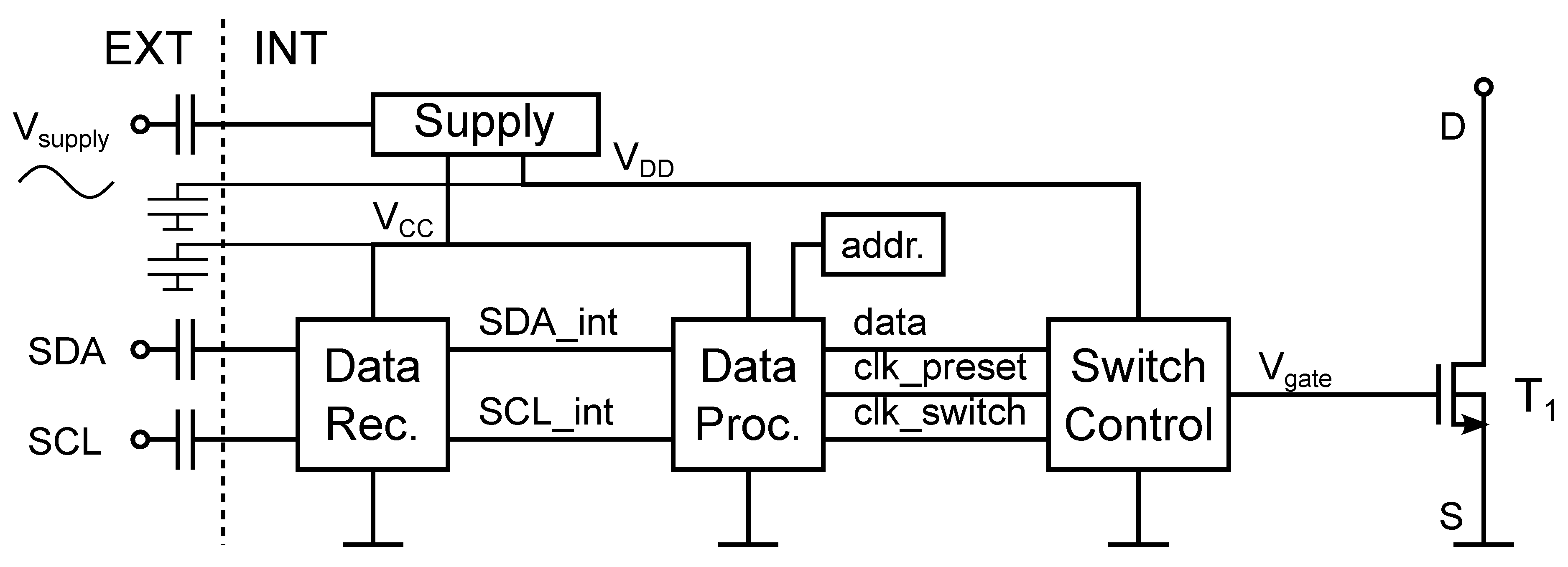
The block diagram of SOMBRA is shown in Figure 2. The isolation capacitors are external. Inside we have a block that controls the supply voltage, a Data Recovery block, a Data Processing block, a Switch Control block, and of course the large switch itself (). is the large N(D)MOS that will conduct the total panel currently. The bulk is connected to the source (S), resulting in a parasitic parallel p-n junction from source to drain (D). This is not an issue in this implementation, as the switch only needs to block current in the direction from drain to source. (Section 2.2.4 also provides an implementation if this were not the case). The source connection will also act as the reference voltage for the entire chip. Activating and deactivating the switch is then as easy as providing a high and low voltage at the gate of ().

Figure 2.
The block diagram of SOMBRA. It consists of a large switch , Voltage Supply block, Data Recovery block, Data Processing block and Switch Control block. The insulation capacitors are external.
The internal circuitry is isolated from the external signals by HV capacitors. The internal voltage supply can be created by applying an AC signal to the pin. Two separate supply voltages are created: and . will only be active when is active (e.g., when receiving data, see below). has to maintain a high voltage even when is no longer powered in order to maintain the gate voltage for . In other words, some parts of the chip will be powered down when not in use. External storage capacitors are optional for , but necessary for .
The communication with the central unit is achieved through a modified version of the IC protocol. Due to the limitations imposed by insulation capacitors, communication is only one way. The central unit can control the switch, but information cannot be sent back. Those capacitors will also distort the signals. Before we can send them to the processing unit (DataProc), they need to pass through a signal reconstruction block (DataRec) to map them to a digital signal the processing unit understands.
The outputs of the DataProc control Switch Control, which drives the gate of . DataRec and DataProc are supplied by and will be powered down in between commands. The time period that the voltage can be maintained depends on the external storage capacitor. This can be optimized together with the configuration update frequency.
2.2.2. Data Communication and Processing
Every SOMBRA chip in the panel has its own reference voltage, but is receiving data from the same central unit with a reference voltage that can be a lot lower (e.g., 10 V). To ensure that DataProc receives CMOS compatible logic levels, isolating capacitors (1 nF) are placed at the inputs, followed by a data recovery circuit (DataRec, see Figure 3). The diodes keep the internal signal () clamped between the supply voltage () and ground. The HV diodes adjust for the difference in internal and external reference voltage (see below), the series of regular diodes filter out any excessive voltages peaks. The subsequent buffer further cleans up the digital signal.
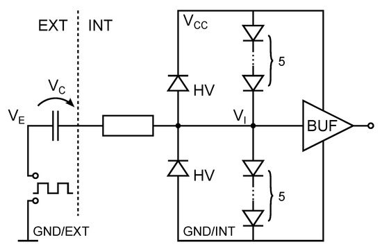
Figure 3.
Schematic of DataRec.
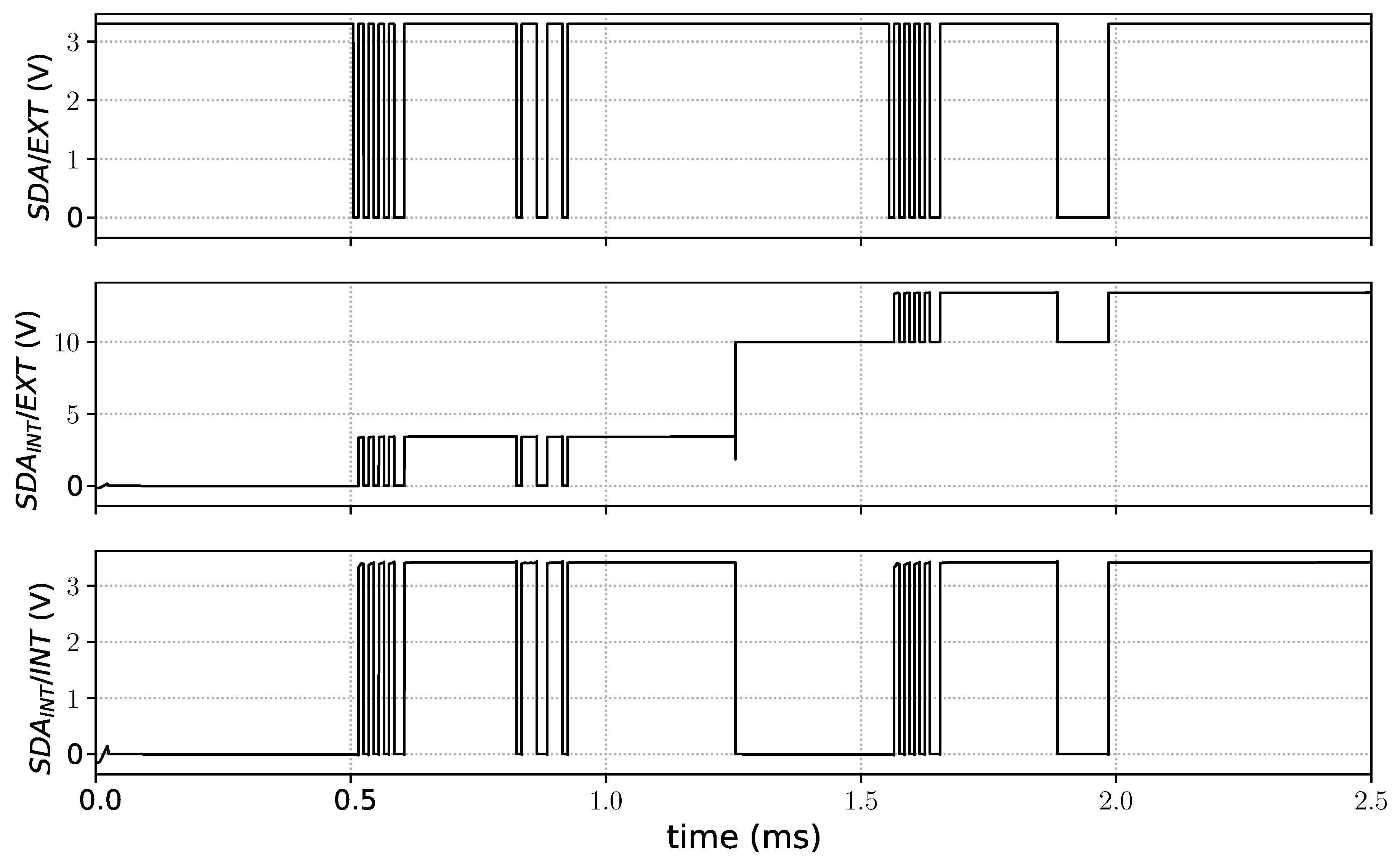
There is one thing that should be taken into account, though. For the data to be received correctly, the voltage over the capacitor, , should be equal to the potential difference between the two reference voltages (). Only then will both a rising edge and a falling edge on the external signal, , be translated into a rising edge and a falling edge on the internal signal, . Let’s elaborate with a small example, assuming V and V. Due to a change in panel configuration, the internal reference voltage, GND/INT, rises to 10 V. The HV clamping diode holds at GND/INT (diode threshold not taken into account). At this point, V. As is still at GND/INT, a falling edge on will not result in a falling edge on . As the start of a new data stream in the IC protocol is indicated by a falling edge, this would result in a missed data sequence. However, a low signal on now changes to equal GND/INT-GND/EXT: a next rising edge on is followed by and a subsequent falling edge on is again translated correctly. Analogous reasoning can be applied when GND/INT suddenly drops in voltage. So before actually starting the data stream, needs to be calibrated. This can be done by sending the data sequence [10101010]. This should happen every time there is a change in panel configuration. It is clear that the internal reference voltage (and thus the panel configuration) should not change when data is being received. Therefore the option is introduced to first send all data to all the switches before changing the states of the switches simultaneously. Figure 4 shows the simulation results of DatRec using the SDA line of the IC protocol. The external signal can be seen on top. At ms, the internal reference voltage jumps to 10 V. The middle signal shows the internal SDA signal with respect to the external reference voltage. The bottom signal shows how SOMBRA sees this internal SDA signal. The bitrate is 100 kbps.

Figure 4.
Simulation of DataRec using the SDA line of the inter-integrated circuit (IC) protocol. At ms the internal reference voltage is changed. (top) The external SDA signal. (middle) Internal SDA signal wrt. the external reference voltage. (bottom) The internal SDA signal vs. the internal reference voltage.
After the signals have been cleaned up, they are ready for DataProc. This is a purely digital block, consisting of an IC slave and a state machine. It was written in Verilog, which was then used to synthesize the netlist and generate the layout compatible with the used technology. DataProc uses an internal clock of about 2.5 MHz, generated by a simple inverter ring as an oscillator.
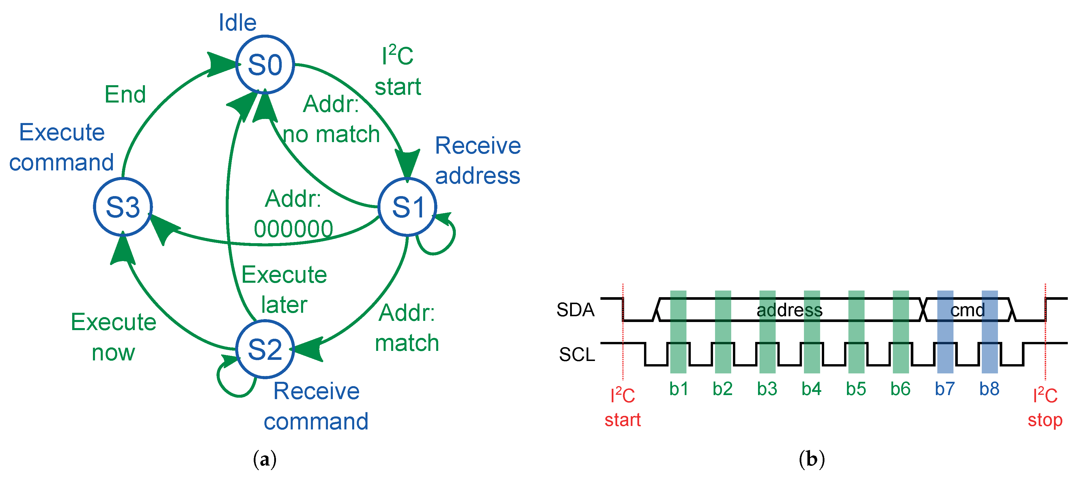
As mentioned before, the communication protocol is loosely based on the IC protocol. It uses two signal lines, SDA (data line) and SCL (clock line). Data can be read when the clock signal is high; data is changed when the clock signal is low. The start and end of an IC data stream are indicated by a rising and falling edge respectively on the SDA line while the SCL line remains high (See Figure 5b). The data stream itself contains eight bits, where six bits of which are used for the address, two bits contain the command. The address space consists of 62 addresses ( special addresses, see below). In the command b8 tells SOMBRA whether the switch should be activated (1) or deactivated (0), indicates whether this should be done immediately (1) or wait for the general command (0). The latter is used when we first send all data to all switches, and only then change their state simultaneously by sending a ‘general command’ [000000]. This behavior is reflected in the state machine of Figure 5a. State is the idle state, where DataProc is powered up, but no data has been received. At the start of an IC sequence, we move to state , where the complete address is received. If the address matches, the command is received in state S2. If the command does not have to be executed immediately, we store the new switch state locally (see also Section 2.2.4) and return to the idle state. In the other case, we move to state where the state of the switch is changed, before returning to the idle state. If in-state address [000000] is received, we immediately skip to where the state of the switch is changed according to the previously stored value. By now it is clear that both address [000000] (the ‘general command’) and address [101010] (sequence used to calibrate ) cannot be used. The former leads to immediate command execution, the latter is a calibration sequence for and is ignored.
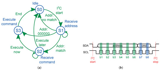
Figure 5.
The DataProc is written as a state machine. Transitions between the states depend on the received data. (a) The state machine in DataProc. (b) Schematic representation of the I2C based communication protocol.
2.2.3. Voltage Supply
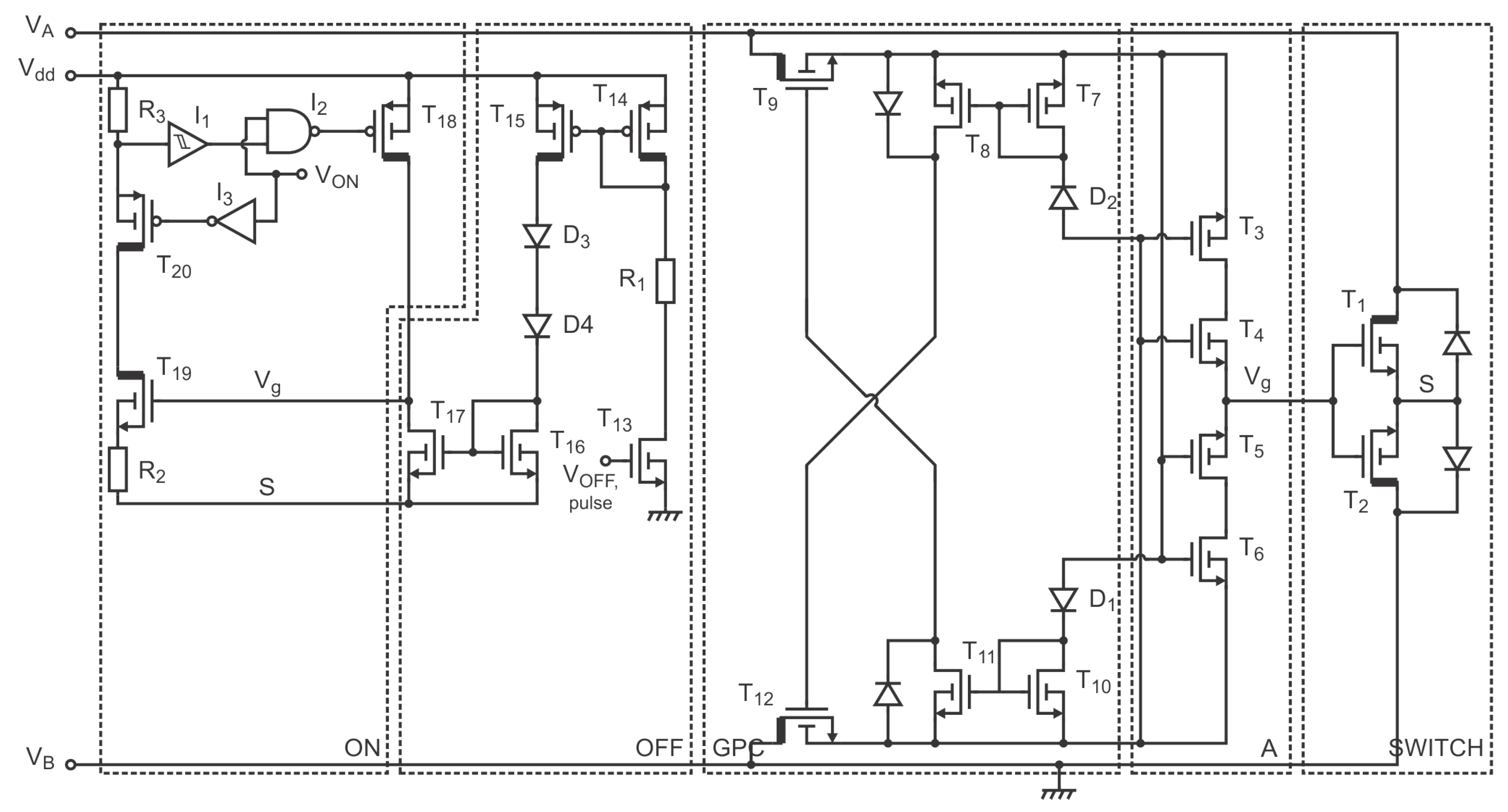
The voltage supply is basically the final stage of a Dickson charge pump (See Figure 6), but with an AC wave input to reduce voltage spikes. and have their own separate charging circuit. has minimal leakage current and can maintain its voltage (and thus the switch state) without for a couple of seconds with an external 1 F capacitor. will be immediately discharged when is not present, powering down DataRec and DataProc. Both and are equipped with a power-on-reset (PoR) circuit which resets everything when their respective parts are powered up. The memory elements in Switch Control are reset to 0, keeping the switch inactive when SOMBRA is powered up.
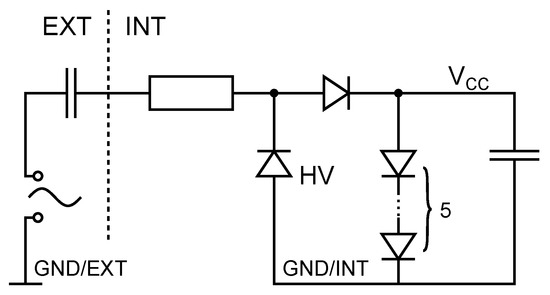
Figure 6.
Schematic of the Voltage Supply.
2.2.4. Switch and Switch Control
As explained in Section 2.1, we need an HV and an LV version of SOMBRA. The difference between these two is mainly expressed in and to a lesser extent in switch control, driving . We wanted to limit the power dissipation in the switch to 0.5 W at maximum. The choices we made and the actual implementation are discussed in the next section.
Switch control itself is fairly straightforward. It consists of two single-bit memory elements (flip-flops) and a buffer driving the gate of . This buffer needs to be adjusted for the gate capacitance of , which differs between the different versions. One flip-flop holds the value of the current state of the switch and can be changed when clk_switch (see Figure 2) is clocked. The other flip-flop holds the value of the next state of the switch and is clocked into the first flip-flop using clk_preset. Both flip-flops are powered with meaning they’ll hold their value even without .
While it was clear that only needed to block current from drain to source and a rather simple driving circuit would suffice, we also designed a switch and its control where this is not the case. Here we need to N(D)MOSes back to back and a more complicated driving circuit (See Figure 7).
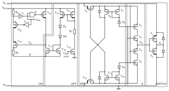
Figure 7.
Schematic of the bidirectional switch and its control.
We assume that the voltage over the device () can vary from minus 40 V to 40 V. In order to be able to block current in both polarities, two N-channel drain-extended metal-oxide-semiconductor field-effect transistor (NDMOS) are placed in anti-series with a common source. Due to the internal body diode (drawn in the figure), this common source voltage follows the lowest voltage of and , making sure that either or is effectively blocking and not breaking down. Circuit A will keep the switch off, even with changing polarities. The common gate of and () is always pulled to the lowest potential between and . The Gate Protection Circuit (GPC) protects the gates in circuit A from overvoltage (>3.6 V): when current flows through ( is rising), the gate-source voltage of is about 2 diode thresholds, pulling to . Current mirror will deactivate , disconnecting the gates of from and thus protecting them when rises further. A symmetric circuit is activated when drops below , disconnecting the gates of from .
We use as the reference voltage for the entire circuit. can thus be positive of negative referenced to this. The switch is turned on by circuit ON. As S follows the lowest voltage, this will always be 0 V () or lower (). In case of the former, is connected to through , activating the switch. In case of the latter, (switch not active) and when turning on the switch, we must make sure that the gate-source voltage () does not exceed 3.6 V. This is achieved by the extra control circuit in ON. produces a current in , which produces a voltage drop over . This voltage drop is sensed with a Schmitt trigger and is disabled accordingly, stopping from charging further, keeping the gate-source voltage of below 3.6 V.
The switch is turned off by pulsing . This causes to pull current from the gate, deactivating the switch. As long as and are active, S cannot freely move, which is why needs to be pulsed. If after deactivating the switch , S stays at 0 V and Circuit A will function immediately. When , S needs to follow . Diodes make sure that S (and ) can become negative enough to activate Circuit A.
As there are now two NDMOSes in the current path ( and ) both of them need a resistance that is half that of in Figure 2 in order to have the same overall switch resistance. Halving the resistance usually means doubling the die surface area. In other words, this bidirectional switch will be about four times as big as the unidirectional switch.
2.3. Implementation
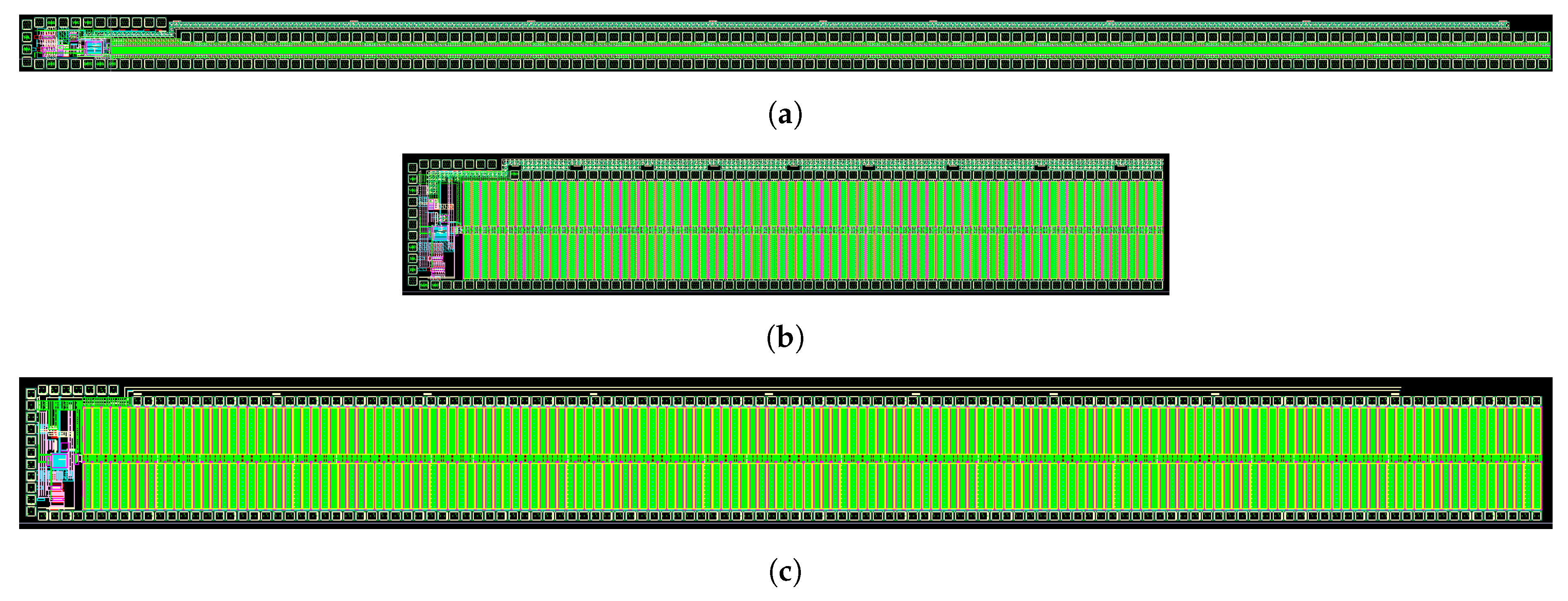
SOMBRA is designed in the I3T50 technology provided by OnSemiconductor. This smart-power IC technology is a 50 V extension of a standard 0.35 m CMOS process. As explained in the previous section, a different version of SOMBRA was designed. SOMBRA-LV10 implements a LV switch for a maximum of 10 A load current. The on-resistance of the N-channel metal-oxide-semiconductor field-effect transistor (NMOS) is the I3T50 technology, which is quite area-effective. SOMBRA-LV10 was designed for an on-resistance of 1.6 m at 27 C (2 m at 85 C). It uses an NMOS with a total channel width of 842,850 m (0.8 m), in total occupying about 9 mm. An image of the layout is shown in Figure 8a. For the HV version, we created SOMBRA-HV05, capable of blocking voltages up to 50 V, but with a maximum load current of 5 A. Because of the lower area efficiency of the HV NDMOS switch, the on-resistance was limited to 7.6 m at 27 C (9.5 m at 85 C). To achieve this, the NDMOS channel width needs to be 1,600,000 m (1.6 m), resulting in a total chip area of 13 mm (See Figure 8b). As a final exercise, we also created SOMBRA-HV10, an HV switch for a 10 A load current. To keep the power dissipation below 0.5 W, the on-resistance was designed for 3.8 m at 27 C (4.8 m at 85 C). The NDMOS channel length would have to be 3,200,000 m (3.2 m) with a total die area of 25 mm (See Figure 8c). It is clear that this last chip is huge, would be very expensive and not economically viable. This version of SOMBRA was not manufactured. Figure 8 shows that the area needed for all other parts of the design (DataRec, DataProc, etc. Located at the very left side of the layout) is negligible compared to the area occupied by the switch itself.
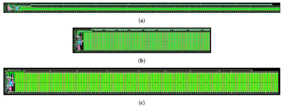
Figure 8.
ayouts of the different version of the SOMBRA chip. (a) SOMBRA-LV10. LV switch for 10 A load current. On resistance: 1.6 mΩ. Total area: 9 mm2. (b) SOMBRA-HV05. HV switch for 5 A load current. On resistance: 7.6 mΩ. Total area: 13 mm2. (c) SOMBRA-HV10. HV switch for 10 A load current. On resistance: 3.8 mΩ. Total area: 25 mm2.
A number of the bond-pads are used to set the IC address of the device. The six bond-pads dedicated to the IC address have an internal pullup resistor of 50 k. Address bits can be set low by connecting the corresponding bond-pad to ground, either externally or internally using bond wires (all the bottom bond-pads are connected to ground).
3. Results
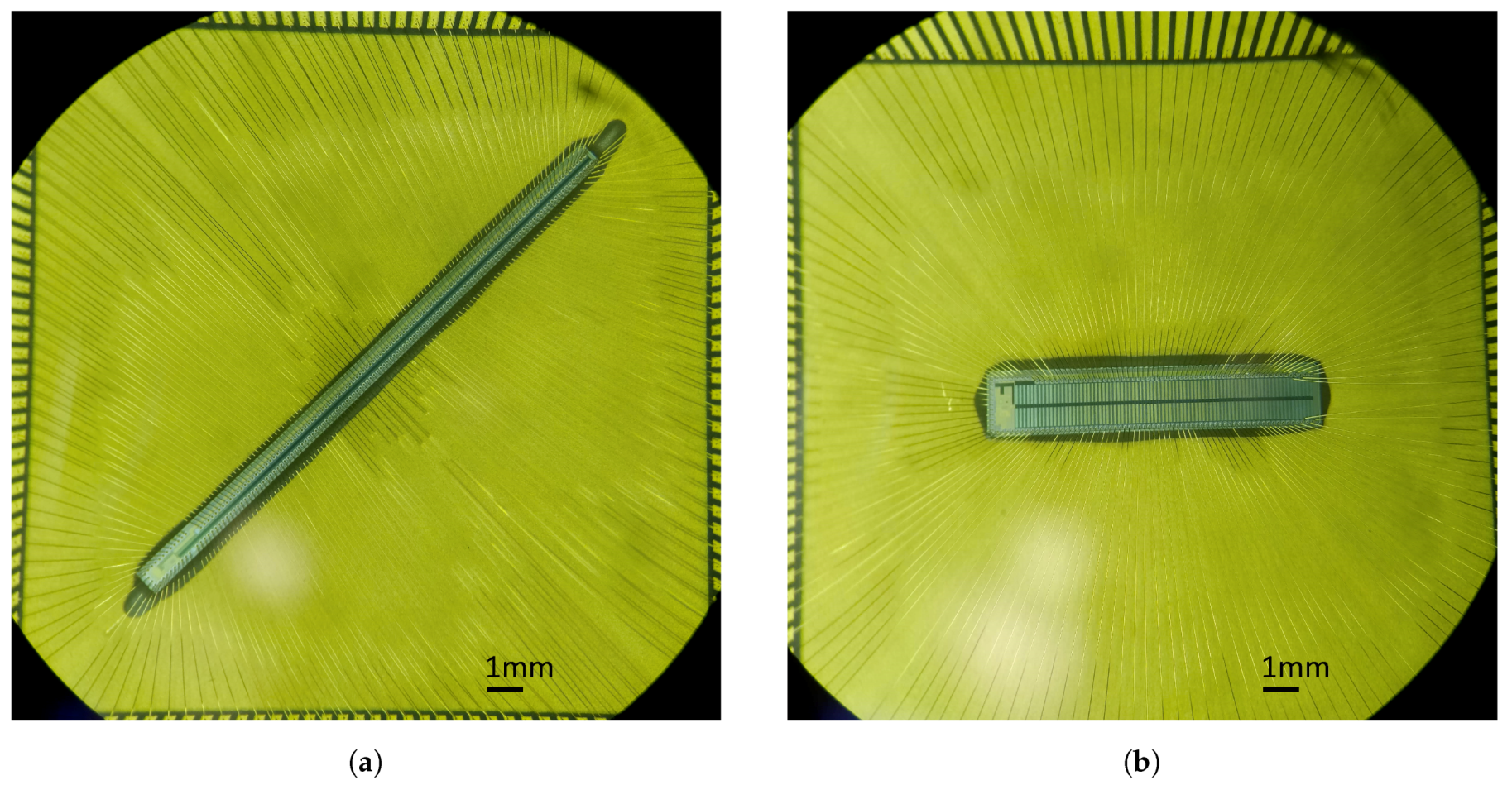
Due to the excessive size of the SOMBRA-HV10 chip, only the SOMBRA-HV05 and SOMBRA-LV10 were physically realized. These two versions can be seen in Figure 9. They are displayed in their pin grid array (PGA) package, chosen for easy pin access. In a real application, other bonding techniques such as flip-chip are probably more suitable. We tested them for functionality and on resistance. Afterward, a very preliminary reconfigurable panel was created and tested. The results will be discussed below.
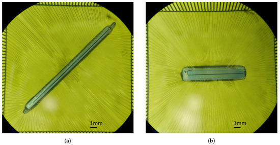
Figure 9.
The two realized SOMBRA versions. (a) SOMBRA-LV10. (b) SOMBRA-HV05.
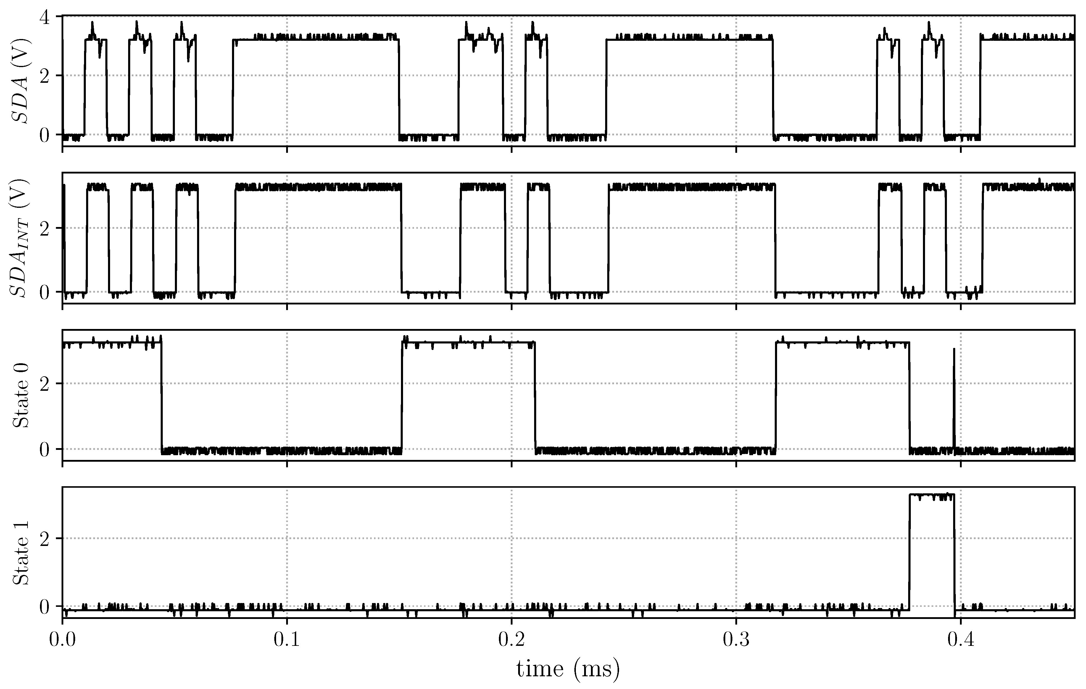
Figure 10 shows the digital signals during a communication sequence (SCL signal not shown). The central unit sends and the received internal signal after data recovery (DataRec) is indicated as . First, the calibration sequence is sent. At ms a data sequence is sent, but the address did not match this SOMBRA’s address. The state machine enters the state [01] (S1) and goes back to the idle state [00] (S0). At about ms, another data sequence arrives, this time with the correct address. After receiving the address, the state machine enters the state [10] (S3) to receive the command. This command is [10], indicating that the switch should be turned off immediately. The command is executed in the state [11] (S4), very quickly at ms.
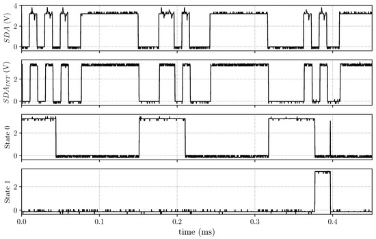
Figure 10.
Measurement of the external and internal communication signals (SDA only) and the resulting effect on the switch’s state machine.
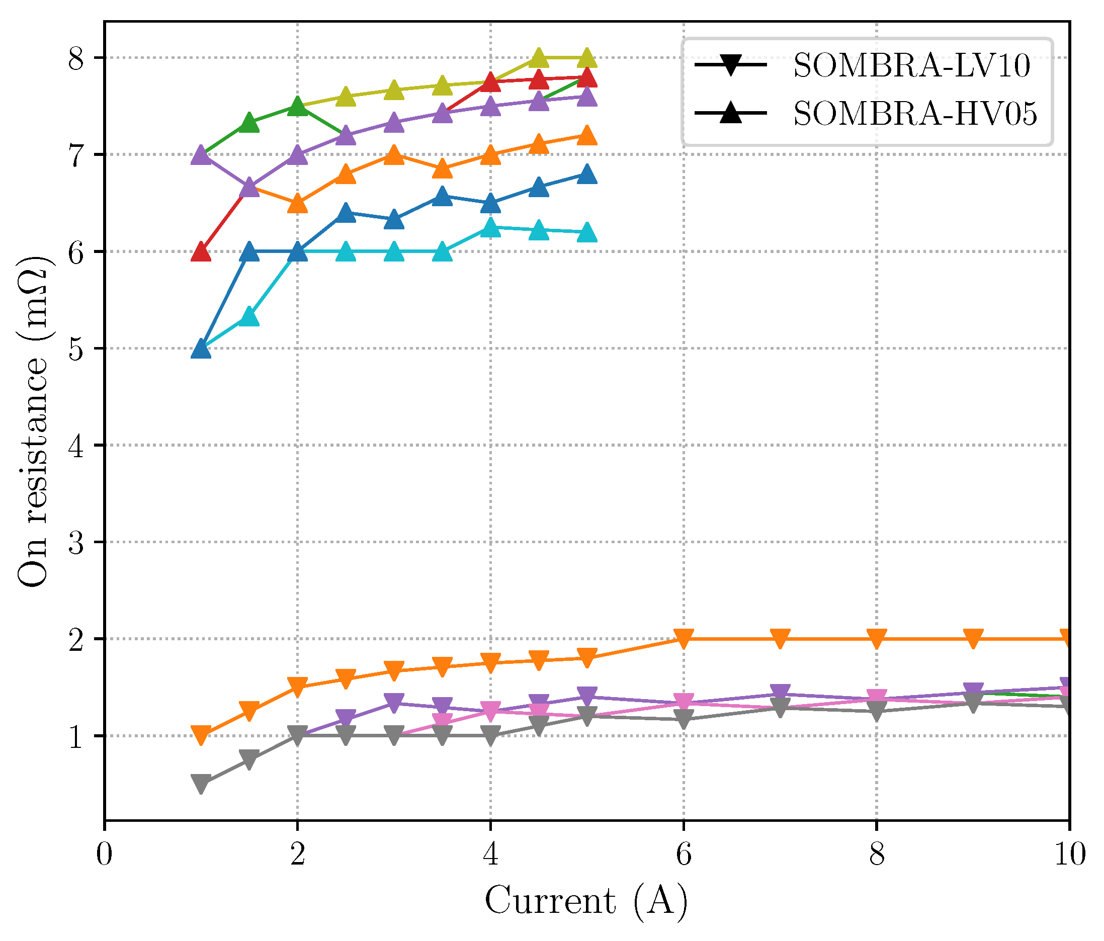
As we are able to successfully turn on (and off) the switches, the on-resistance can be measured. The results are collected in Figure 11. For both SOMBRA-LV10 and SOMBRA-HV05, 10 switches were measured. They both perform somewhat better than designed. For the HV version, we measured an average on-resistance of 7.3 m at the maximum load current of 5 A. The LV version measured an average resistance of 1.3 m at 10 A.
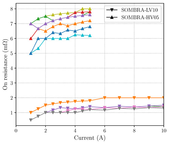
Figure 11.
On resistance measurement. The average on resistance is 7.3 m for SOMBRA-HV05 and 1.3 m for SOMBRA-LV10.
To see how our SOMBRA fares in a reconfigurable panel, a small test setup was created with two substrings of six full cells each. With three SOMBRA switches, it should be possible to connect these substrings in either parallel or series (see Figure 12a). Figure 12b confirm this behavior. These tests were performed under low light conditions, resulting in a maximum output current of 300 mA for a single cell. The oscillations on the measured signal are a result of unstable light output. This is a small-scale, low-power demonstrator. However, from Figure 11 we know that SOMBRA can handle the larger currents and as the operation of the switch itself is independent on the number of cells in the substring, the SOMRBA switch meets the requirements to be used in a full reconfigurable panel.
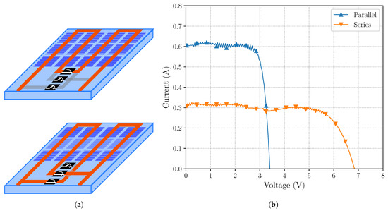
Figure 12.
Setup and measurement result of a small-scale two-substring reconfigurable panel. The two substrings can be connected in either series or parallel. (a) Schematic representation of the test setup. (b) Measurements of the output voltage and current.
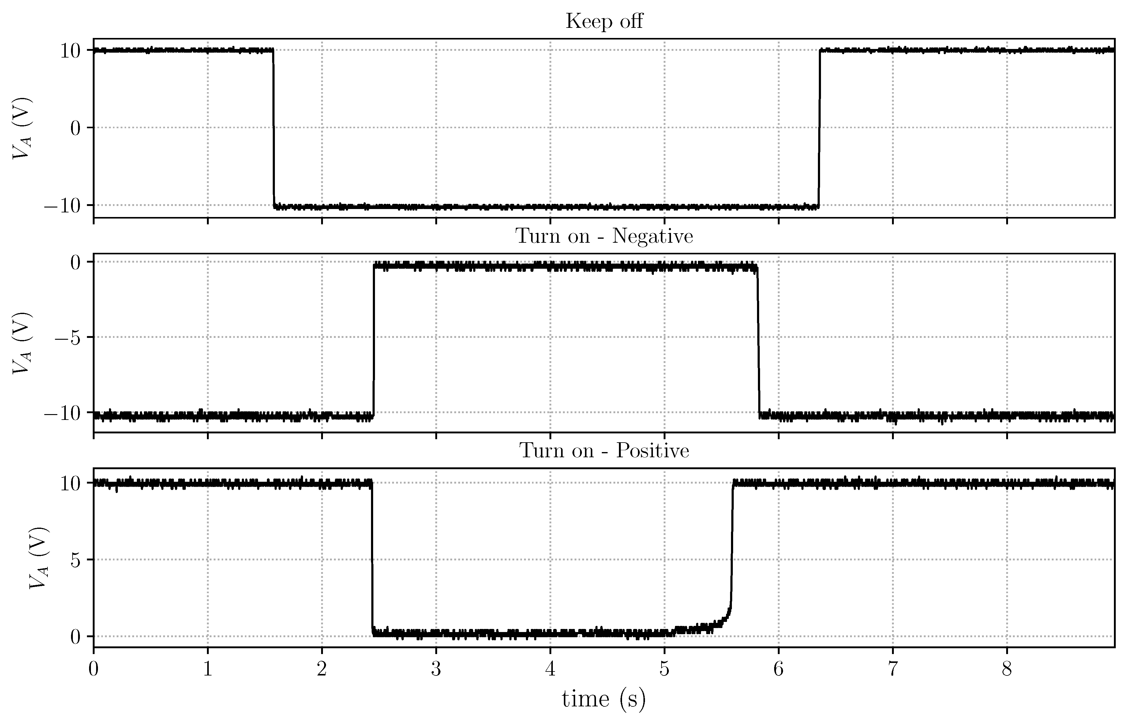
As the last measurement, we examined the bidirectional switch from Figure 7. As explained, the total die area of this switch would be four times as large for the same on-resistance as the unidirectional switch. The version under testing was made with external NDMOSes and the testing was mainly focused on the functionality of the control circuit. Figure 13 proves that the proposed design works as intended. The switch can block HV voltages in both polarities. The switch can successfully be turned on and off under positive () and negative polarity ().
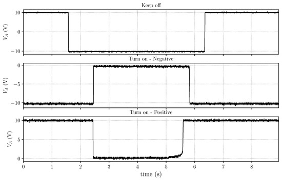
Figure 13.
The bidirectional switch under testing. (top) The switch blocks HV in both polarities. (middle) The switch is turned on and off under negative polarity. (bottom) the switch is turned on and off under positive polarity.
4. Discussion
As the SOMBRA switch is a dedicated design to fit the specific requirements for our reconfigurable PV panel, it is difficult to compare with state-of-the-art. Before testing the setup in Figure 12a with SOMBRA devices, the commercial device IRF7769L1TRPbF was used [26]. This device has an on-resistance of 2.8 m with a maximum load current of 20 A, however, the gate is to be driven directly. Without (isolated) communication protocol this device would not be usable in a full reconfigurable panel setup. As explained in the introduction, there are no commercial devices available that would meet all our requirements.
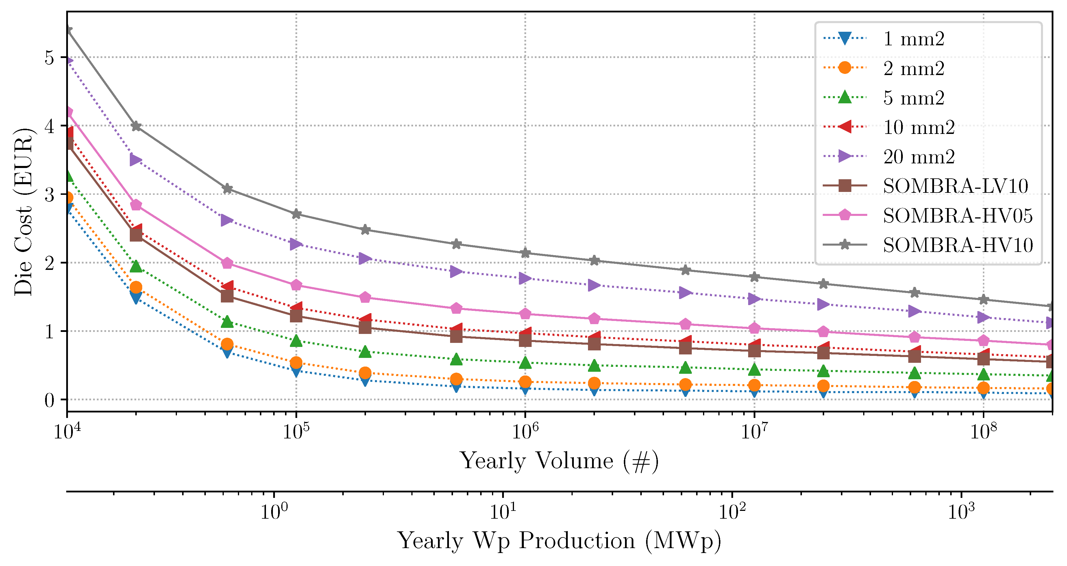
But this begs another question, how economically feasible would the SOMBRA be? SOMBRA is entirely integrated, meaning that the large N(D)MOS is necessarily a planar device: drain and source are located on the same side and the current flows laterally. Especially in the I3T50 technology, this results in very large devices (9 mm and 13 mm for SOMBRA-LV10 and SOMBRA-HV05 respectively, up to 25 mm for the SOMBRA-HV10) resulting in high costs. In order to have a better idea of those costs, Figure 14 displays the projected cost (in EUR) for each die versus the yearly production volume (in the number of devices). Assuming 20 devices per panel and taking 250 Wp per panel, this also corresponds with a yearly Wp production. The cost projection is made for both generic die sizes and the SOMBRA devices specifically.
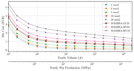
Figure 14.
Chip cost for dies of different sizes versus yearly production volume. Assuming 20 devices and 250 Wp per panel, this can also be expressed as yearly Wp production.
It is immediately clear that when the volume is not high enough, the cost would be too high. A yearly volume of 10 million devices (125 MWp production) would drop the price to 0.75 EUR for SOMBRA-LV10 and 1.00 EUR for SOMBRA-HV05, but the SOMRBA-HV10 would still be 2.00 EUR. We would have to go for a volume of 100 million devices (1.25 GWp) to let the latter drop to 1.50 EUR, with the other devices ending up at 0.50 EUR and 0.80 EUR. These benefit less from the extra volume. Especially for the HV versions, this is still quite expensive. When 20–30 SOMBRA switches are needed for a single panel, this already adds 40 EUR–50 EUR to its cost. Together with the other necessary components, this figure will rise even more. Given the fact that we’re aiming here at residential installations (BAPV, BIPV), this relatively large extra cost compared to the standard panel cost [27] might put people off from investing in such a panel. If we would be able to prove that the expected return (in terms of increased energy output per panel) is worth more than this extra cost, we would have a stronger case, but at this time we cannot provide such proof.
There are several options to work around this issue. Firstly, we could take a look at other chip technologies. There might be technologies that are better suited for these high-voltage, high-current applications, or technologies that are more area efficient. Although newer and more complex technologies will probably be more expensive as well. Secondly, we could step away from a fully integrated switch and go back to a system in package (SiP) approach. There are very low-ohmic, very cheap NDMOSes available. These are usually vertical devices: drain and source are at opposite sides of the die, and the current flows vertically. Because the bottom side of the die is now a contact, these devices cannot be integrated with other circuitry on that same die. With the large N(D)MOS () external, SOMBRA would fit on a die of merely 0.5 mm, resulting in a lower cost, which drops quickly even with lower volumes. We estimate that such a device (SOMBRA plus NDMOS) would average out to about 0.15 EUR. A rudimentary estimation was made to determine the total extra cost of a reconfigurable panel, taking into account the SOMBRAs and packaging, the additional wiring and the four extra (low-cost) DC–DC converters [19] (See Figure 1). The cost associated with changing the wiring of the currently manufactured panels (no panels today can readily be used with this system) is neglected. The estimation brings the total added cost per panel to about 10 EUR. While this is a small cost compared to the total panel cost, long-term on-the-field measurements still need be performed to provide an accurate view of the reconfigurable panel’s energy gain.
5. Conclusions and Future
In this paper, we presented the design and implementation of the SOMBRA switch: an intelligent, integrated switch that can be employed in a reconfigurable PV panel. Such a panel can potentially reduce energy loss due to partial shading. Three versions of SOMBRA were designed. SOMBRA-LV10: a LV (<3.6 V) version for high currents (10 A), SOMBRA-HV05: a HV (<50 V) version for low currents (5 A), and SOMBRA-HV10: a HV version for high currents. Of those three, the two former versions are realized. Measurements proved them to be functional and showed an on resistance of 1.3 m for SOMBRA-LV10 and 7.3 m for SOMBRA-HV05.
While the first preliminary tests looked promising, a lot of development still needs to be done for a functional full-scale prototype. This full-scale reconfigurable panel needs to be made and tested. The control algorithm, which finds the optimal panel configuration for the current shading scenario and accordingly decides which switches should be activated, needs to be designed. Only then can we progress to a long-term measurement to asses the actual energy gain of such a reconfigurable panel. In parallel to this, a more economically viable design of the SOMBRA switch should be examined. Also, before moving on to an actual product, topics such as maintenance and reliability should be discussed. As of now, failure of a single SOMBRA switch can lead to failure of the entire system and might put dangerous stress on other components when unchecked.
Author Contributions
The author contributions for this article are as follows: conceptualization, P.B. and J.D.; investigation, P.B.; validation, P.B.; writing—original draft preparation, P.B.; writing—review and editing, P.B. and J.D.; funding acquisition, J.D.; supervision, J.D.
Funding
This research is part of the SmartPV project. The SmartPV project is an IWT-SBO project, sponsored by the Flemish government. The project partners are imec, Ghent University, the University of Leuven and VITO.
Conflicts of Interest
The authors declare no conflict of interest. The founding sponsors had no role in the design of the study; in the collection, analyses or interpretation of data; in the writing of the manuscript; nor in the decision to publish the results.
Abbreviations
The following abbreviations are used in this manuscript:
| BAPV | Building applied PV |
| BIPV | Building integrated PV |
| HV | High-voltage |
| IC | Inter-integrated circuit |
| LV | Low voltage |
| MPP | Maximum power point |
| MPPT | Maximum power point tracker |
| NMOS | N-channel metal-oxide-semiconductor field effect transistor |
| NDMOS | N-channel drain-extended metal-oxide-semiconductor field effect transistor |
| PGA | Pin grid array |
| PoR | Power-on-reset |
| PV | Photovoltaics |
| SiP | System in package |
| SOMBRA | Switch for the optimization of module power by reconfiguration of all strings |
| TCT | Totally cross tied |
References
- Shockley, W.; Queisser, H.J. Detailed Balance Limit of Efficiency of p-n Junction Solar Cells. J. Appl. Phys. 1961, 32, 510–519. [Google Scholar] [CrossRef]
- Richter, A.; Hermle, M.; Glunz, S.W. Reassessment of the Limiting Efficiency for Crystalline Silicon Solar Cells. IEEE J. Photovolt. 2013, 3, 1184–1191. [Google Scholar] [CrossRef]
- Green, M.A.; Dunlop, E.D.; Levi, D.H.; Hohl-Ebinger, J.; Yoshita, M.; Ho-Baillie, A.W. Solar cell efficiency tables (version 54). Prog. Photovolt. Res. Appl. 2019, 27, 565–575. [Google Scholar] [CrossRef]
- Silvestre, S.; Chouder, A. Effects of Shadowing on Photovoltaic Module Performance. Prog. Photovolt. Res. Appl. 2008, 16, 141–149. [Google Scholar] [CrossRef]
- García, M.C.A.; Herrmann, W.; Böhmer, W.; Proisy, B. Thermal and Electrical Effects Caused by Outdoor Hot-Spot Testing in Associations of Photovoltaic Cells. Prog. Photovolt. Res. Appl. 2003, 11, 293–307. [Google Scholar] [CrossRef]
- Hermann, W.; Wiesner, W.; Vaaßen, W. Hot Spot Investigations on PV Modules—New Concepts for a Test Standard and Consequences for Module Design with Respect to Bypass Diodes. In Proceedings of the 26th IEEE Photovoltaic Specialist Conference, Anaheim, CA, USA, 30 September–3 October 1997; pp. 1129–1132. [Google Scholar]
- Bauwens, P.; Doutreloigne, J. Reducing Partial Shading Power Loss with an Integrated Smart Bypass. Sol. Energy 2014, 103, 134–142. [Google Scholar] [CrossRef]
- Bauwens, P.; Doutreloigne, J. NMOS-Based Integrated Modular Bypass for Use in Solar Systems NIMBUS: Intelligent Bypass for Reducing Partial Shading Power Loss in Solar Panel Applications. Energies 2016, 9, 450. [Google Scholar] [CrossRef]
- Villa, L.F.L.; Picault, D.; Raison, B. Maximizing the Power Output of Partially Shaded Photovoltaic Plants Through Optimization of the Interconnections Among its Modules. IEEE J. Photovolt. 2012, 2, 154–163. [Google Scholar] [CrossRef]
- Karatepe, E.; Boztepe, M.; Çolak, M. Development of a Suitable Model for Characterizing Photovoltaic Arrays with Shaded Solar Cells. Sol. Energy 2007, 81, 977–992. [Google Scholar] [CrossRef]
- Mäki, A.; Valkealahti, S.; Leppäaho, J. Operation of Series-Connected Silicon-Based Photovoltaic Modules under Partial Shading Conditions. Prog. Photovolt. Res. Appl. 2012, 20, 298–309. [Google Scholar] [CrossRef]
- Patel, H.; Agarwal, V. MATLAB-Based Modeling to Study the Effects of Partial Shading on PV Array Characteristics. IEEE Trans. Energy Convers. 2008, 23, 302–310. [Google Scholar] [CrossRef]
- Woyte, A.; Nijs, J.; Belmans, R. Partial Shadowing of PhotoVoltaic Arrays with Different System Configurations: Literature Review and Field Test Results. Sol. Energy 2003, 74, 217–233. [Google Scholar] [CrossRef]
- Alsayida, B.; Alsadi, S.; Jallad, J.; Dradi, M. Partial Shading of PV System Simulation with Experimental Results. Smart Grid Renew. Energy 2013, 4, 429–435. [Google Scholar] [CrossRef]
- Reisi, A.R.; Moradi, M.H.; Jamasb, S. Classification and comparison of maximum power point tracking techniques for photovoltaic system: A review. Renew. Sustain. Energy Rev. 2013, 19, 433–443. [Google Scholar] [CrossRef]
- Baka, M.I.; Catthoor, F.; Soudris, D. Near-Static Shading Exploration for Smart Photovoltaic Module Topologies Based on Snake-like Configurations. ACM Trans. Embed. Comput. Syst. 2016, 15, 27. [Google Scholar] [CrossRef]
- Bauwens, P.; Govaerts, J.; Baka, M.; Catthoor, F.; Baert, K.; den Broeck, G.V.; Goverde, H.; Anagnostos, D.; Doutreloigne, J.; Poortmans, J. Reconfigurable Topologies for Smarter PV Modules: Simulation, Evaluation and Implementation. In Proceedings of the 32nd European Photovoltaic Solar Energy Conference and Exhibition, Munich, Germany, 20–24 June 2016; pp. 61–65. [Google Scholar]
- Poortmans, J.; Baert, K.; Govaerts, J.; Mertens, R.; Catthoor, F.; Germain, M.; Das, J.; Driessen, J. Linking Nanotechnology to Gigawatts: Creating Building Blocks for Smart PV Modules. Prog. Photovolt. Res. Appl. 2011, 19, 772–780. [Google Scholar] [CrossRef]
- Bauwens, P.; Bakovasilis, A.; Manganiello, P.; Voroshazi, E.; Doutreloigne, J.; Poortmans, J.; Catthoor, F. Switched- Capacitors as Local Converters for Snake PV Modules: A Cost/Efficiency Exploration. In Proceedings of the 35th European Photovoltaic Solar Energy Conference and Exhibition, Brussels, Belgium, 24–28 September 2018; pp. 1127–1130. [Google Scholar]
- Analog Devices. LTM9100 Datasheet. Available online: https://www.analog.com/media/en/technical-documentation/data-sheets/9100f.pdf (accessed on 31 October 2019).
- Ribarich, T.; Zhang, J. Power FET Driver. United States 10044350. 2018. Available online: https://patentscope.wipo.int/search/en/detail.jsf?docId=US224255206 (accessed on 31 October 2019).
- O’Brien, M. Designing Robust, Isolated I2C/PMBus Data Interfaces for Industrial, Telecommunications, and Medical Applications; Technical Report; Analog Devices: Norwood, MA, USA, 2014; Available online: https://www.analog.com/media/en/analog-dialogue/volume-48/number-3/articles/designingrobust-isolated-i2c-pmbus.pdf (accessed on 31 October 2019).
- Martins, D.; Kruck, A.M. Optical Isolator for I2C Bus System; Technical Report; Vishay Semiconductors: Taguig, Philippines, 2018; Available online: http://www.vishay.com/docs/84901/opticalisolatorfoti2cvussystem.pdf (accessed on 31 October 2019).
- Vishay Semiconductor. VO0661 Datasheet. Available online: https://www.vishay.com/docs/84607/vo0600t.pdf (accessed on 31 October 2019).
- Texas Instruments. ISO154x Datasheet. Available online: http://www.ti.com/lit/ds/symlink/iso1540-q1.pdf (accessed on 31 October 2019).
- Infineon. IRF7769L1TRPbF Datasheet. Available online: https://www.infineon.com/dgdl/Infineon-IRF7769L1-DS-v02_00-EN.pdf?fileId=5546d462533600a4015356079bd91cb4 (accessed on 31 October 2019).
- Solar Power Europe. Global Market Outlook For Solar Power/2019–2023. Available online: https://www.solarpowereurope.org/wp-content/uploads/2019/05/SolarPower-Europe-Global-Market-Outlook-2019-2023.pdf (accessed on 31 October 2019).


© 2019 by the authors. Licensee MDPI, Basel, Switzerland. This article is an open access article distributed under the terms and conditions of the Creative Commons Attribution (CC BY) license (http://creativecommons.org/licenses/by/4.0/).