Article

High-Efficiency Bidirectional LLC Resonant Converter with Primary Auxiliary Windings

Department of Electrical and Electronics Engineering, JeonJu University, JeonJu 55069, Korea
*
Author to whom correspondence should be addressed.
Energies 2019, 12(24), 4692; https://doi.org/10.3390/en12244692
Submission received: 29 September 2019 / Revised: 5 December 2019 / Accepted: 9 December 2019 / Published: 10 December 2019
(This article belongs to the Special Issue Advanced in Resonant Converter and Dual Active Bridge Converter)

Abstract

:
In this paper, high-efficiency bidirectional LLC resonant converters with primary auxiliary windings in transformers of resonant circuits are proposed. Even though resonant capacitors are used on the primary and secondary sides, the proposed converter can operate, regardless of the direction of the power flow, with the high gain characteristics of the LLC resonant converter without the mutual coupling of resonant capacitors. The operation principles and gain characteristics of the proposed bidirectional DC–DC converters are described in detail. A 3.3 kW prototyped bidirectional LLC resonant converter for interfacing 750 VDC buses was built and tested to verify the effectiveness and applicability of this proposed converter.

1. Introduction

Voltage source-isolated or current source-isolated bidirectional DC–DC converters using a high-frequency transformer are generally used in energy storage systems for renewable energy sources and future electric vehicles [1,2,3]. To achieve a highly integrated power conversion circuit, the switching frequency should be increased. However, this has the drawback of hard switching, which can cause higher switching losses.
Recently, to minimize the size, switching losses, and Electromagnetic Interference (EMI) of a bidirectional DC–DC converter, CLLC resonant circuits with soft-switching characteristics, as shown in Figure 1a, were developed for the bidirectional DC–DC converter [4,5,6,7]. Due to the use of small resonant capacitors (Cr, CR) in the primary and the secondary sides, the CLLC (CCL+LLC) shows gain characteristics as illustrated in Figure 1c, as compared to the high gain characteristics (at the frequency regions lower than the resonant frequency) of the conventional LLC resonant converter as illustrated in Figure 1b.
In heavy load conditions and frequency regions lower than the resonant frequency, the slope of the CLLC gain characteristics decreases, which means that zero voltage switching (ZVS) cannot be achieved. To increase the CLLC gain slope in frequency ranges below the resonant frequency, the transformer magnetization inductance (Lm) must be significantly reduced, however, improving the efficiency is challenging because of the increase in conduction losses. To operate with the wide range of voltages in the bidirectional power transfer, a two-stage DC–DC converter (as shown in Figure 1a) composed of a hard-switched buck/boost converter for output voltage control and an unregulated LLC converter for electrical isolation has been used in various applications [7]. However, the two-stage bidirectional DC–DC converter not only causes high power losses but results in increased costs.
In this paper, bidirectional LLC resonant converters with a wide input and output voltage range are proposed, as shown in Figure 2 [8]. Compared to the operational characteristics of the conventional bidirectional CLLC resonant converter presented in Figure 1a, the proposed converters can be operated with high gain characteristics without mutual coupling even though resonant capacitors are used on the primary and secondary sides. Therefore, without any additional buck/boost converter, the proposed bidirectional LLC resonant converter can be operated with high gain characteristics as a conventional LLC resonant converter, regardless of the direction of the power flow.
The proposed bidirectional LLC resonant converter 1 (Figure 2a) can be controlled at a nominal voltage that is close to the resonant frequency in the forward operation. However, in the reverse operation, it operates in the high switching frequency range above the resonance frequency with the charged battery voltage. Therefore, to control the charging/discharging voltage range (Vo: 270 VDC–430 VDC) of a battery at the fixed input voltage (VIN: 750 VDC), it is necessary to adjust the gain in the forward and reverse power transfer operations. For this purpose, we propose bidirectional LLC resonant converters with auxiliary windings at the primary side of transformers, as shown in Figure 2b,c. In this paper, a 3.3 kW prototype bidirectional LLC resonant converter (Figure 2c) was designed and tested to confirm the validity and applicability of the proposed converter.

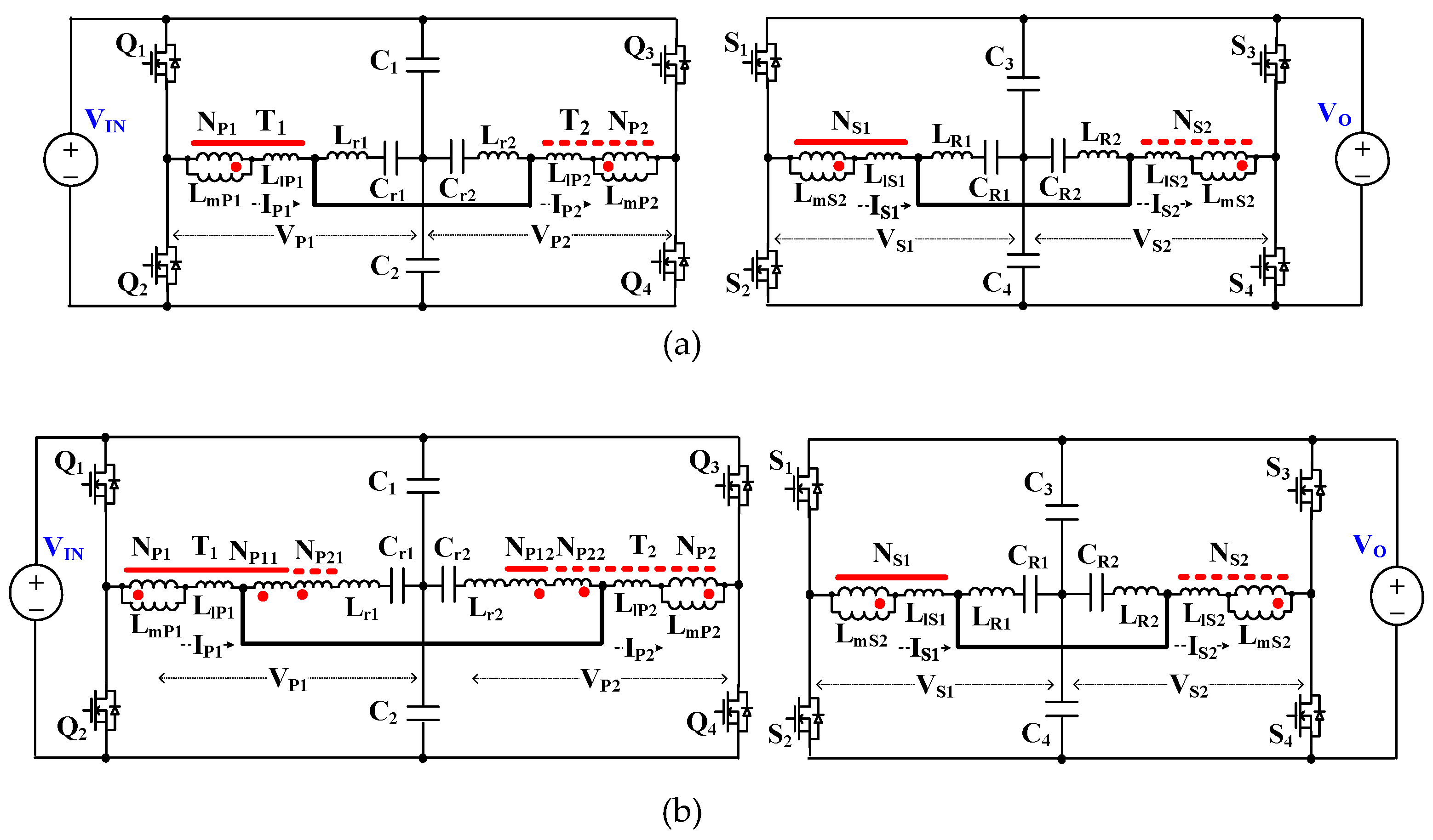
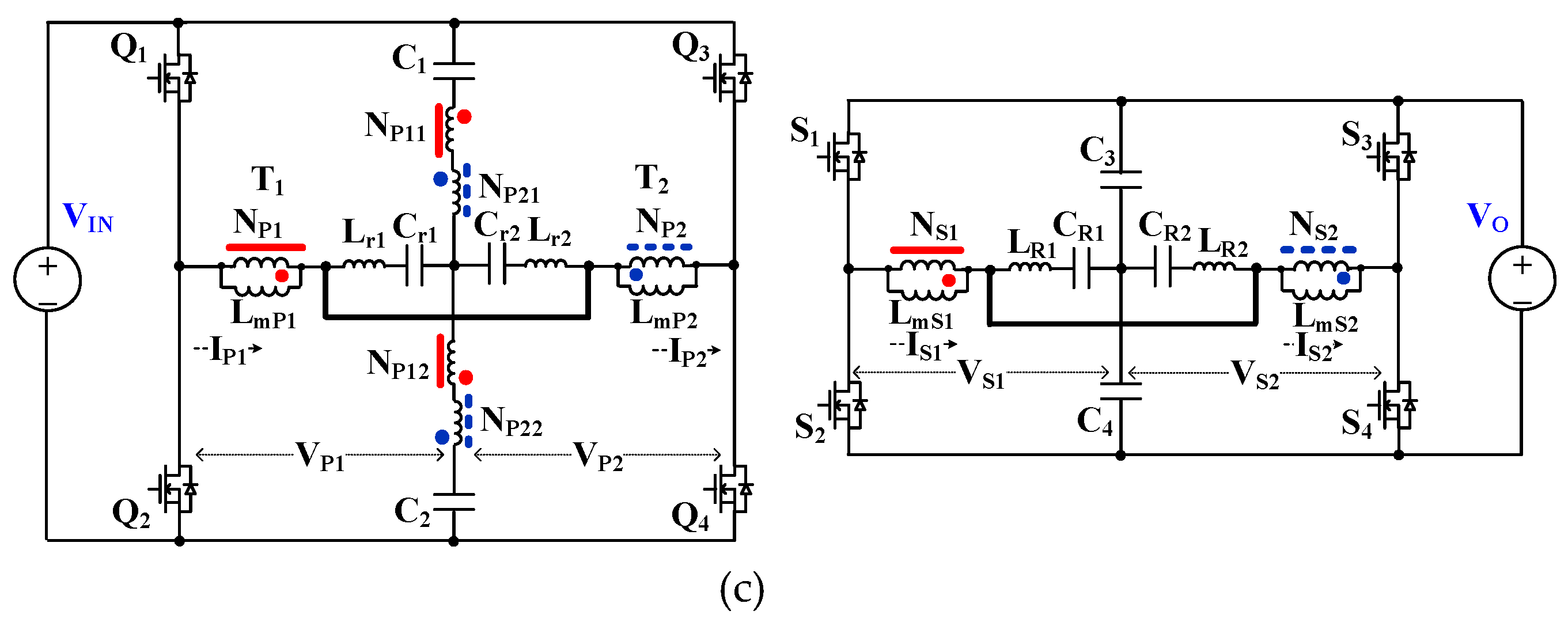
2. Proposed Bidirectional LLC Resonant Converter

The proposed bidirectional LLC resonant converter shown in Figure 2c has two independent resonant circuits comprised of two transformers (T1, T2) including the primary main windings (NP1, NP2) with auxiliary windings (NP11/NP12, NP21/NP22), and resonant components (Cr1/Cr2, CR1/CR2 & Lr1/Lr2, LR1/LR2), with common lines and voltage-divided capacitors (C1/C2, C3/C4) on the primary and secondary side. Even though resonant capacitors (Cr1/Cr2, CR1/CR2) are used on the primary and secondary sides, the proposed converters can be operated with the high gain characteristics of LLC resonant converters without mutual coupling. Depending on the status (on/off) of the switches (Q1–Q4/ S1–S4) in the forward and reverse operation mode, the four modes that operate in the discontinuous mode below resonant frequency (fr) are described below.

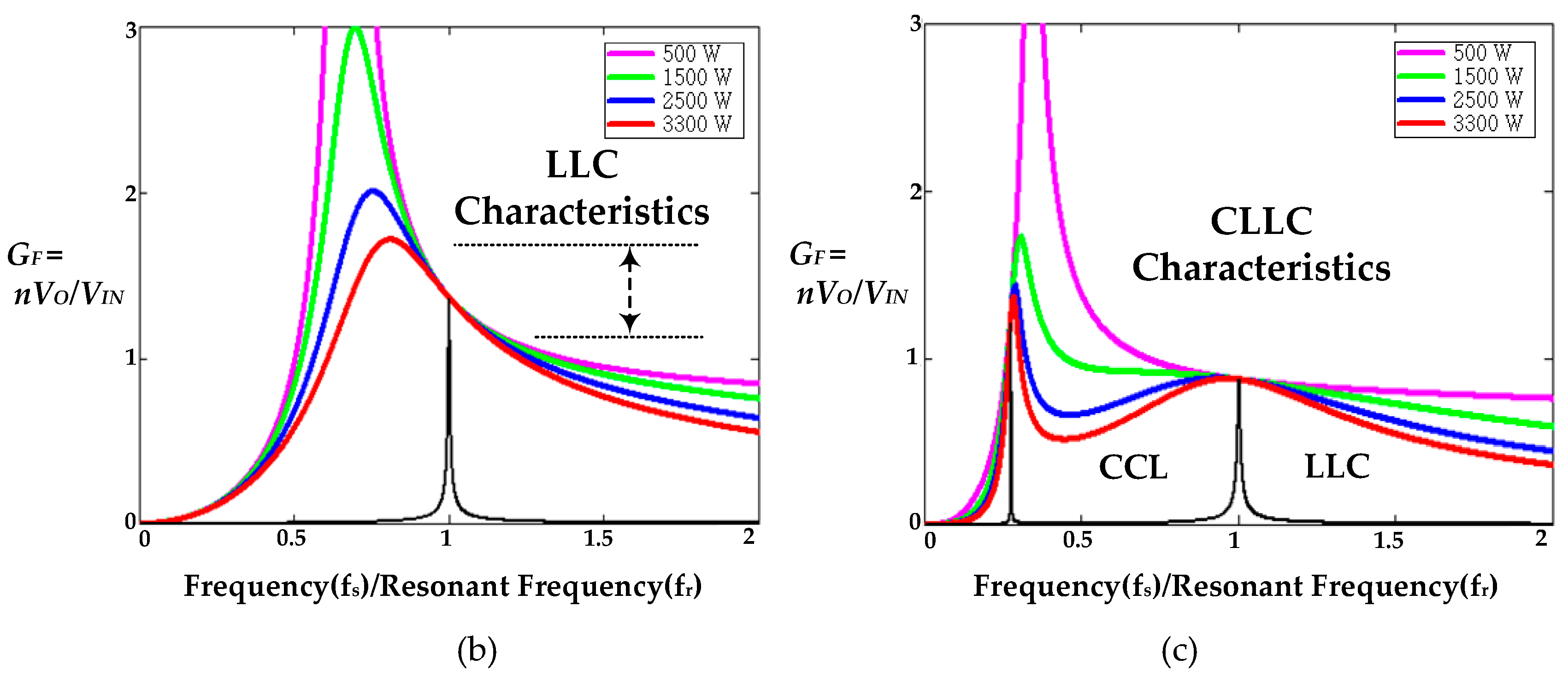
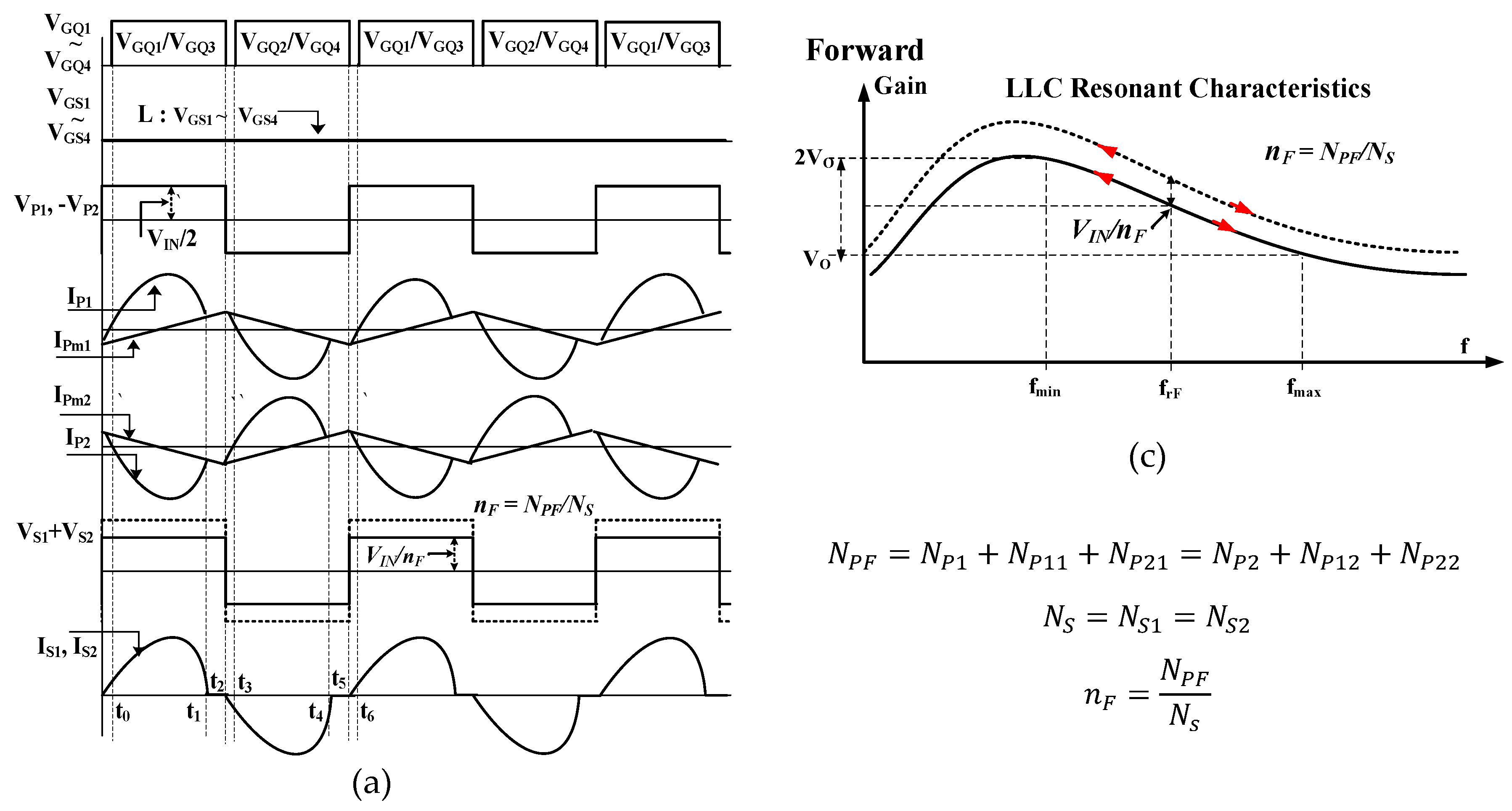
2.1. Forward Operation Mode

In the forward operation mode, as shown in Figure 3a,b, Q1/Q3 and Q2/Q4 are simultaneously turned on and off with a 50% duty cycle. The anti-parallel diodes of the secondary switches (S1/S4, S2/S3) are operated as rectifier diodes since secondary switches (S1, S2, S3, S4) are turned off. During the time interval t0–t1, when the primary switches (Q1/Q3) are turned on with ZVS, half of the input voltage (VIN) is applied to the resonant circuits including the transformer primary main windings (NP1, NP2) and auxiliary windings (NP11–NP21, NP12–NP22), the resonant inductors (Lr1, Lr2) and capacitors (Cr1, Cr2). Moreover, the voltages applied to the primary main windings and auxiliary windings of each transformer (T1, T2), are transferred to the transformer secondary windings (NS1, NS2) by the turn-ratio (nF) of each transformer. As shown in Figure 3c, the turn-ratio (nF) is set to adjust the charging voltage and the frequency control range. Here, the turn-ratio is the ratio of the transformer primary winding (NPF) to the secondary winding (NS) in the forward power transfer operation. At this time, the primary resonant currents IP1(IP2) are flowing with the following paths: the voltage divided capacitor (C1) → Q1(Q3) → primary main windings NP1(NP2) → the resonant inductors Lr1(Lr2) and capacitors Cr1(Cr2) → the auxiliary windings NP11–NP21 → C1, respectively. Furthermore, the primary resonant currents IP1(IP2) are flowing through paths of the input voltage (VIN) → Q1(Q3) → primary main windings NP1(NP2) → the resonant inductors Lr1(Lr2) and capacitors Cr1(Cr2) → the auxiliary windings NP12–NP22 → the voltage divided capacitor (C2), and back to the input voltage (VIN), respectively. If there is a difference in the resonant current (IP1, IP2) flowing in each resonant circuit, the current flows through the primary common connection line by the voltage difference charged in the resonant capacitors (Cr1, Cr2) to suppress the resonant current unbalance. Due to the voltage polarity of secondary windings (NS1/NS2) in transformers (T1, T2), the sum voltage (VS1+VS2) of the secondary windings is transferred to the output side.
Furthermore, the secondary resonant currents (IS1, IS2) do not flow through the secondary resonant capacitors (CR1, CR2), but flow through the secondary common connection line and anti-parallel diodes of the secondary switching devices (S2/S3, S1/S4). Therefore, even when resonant capacitors are used on the primary and secondary sides, the proposed converter can operate with the high gain characteristics of the LLC resonant converter without mutual coupling. In the interval t1–t2, the primary switches (Q1/Q3) are kept turned on, which may look similar to the operation mode of the time interval t0–t1. However, interval t1–t2 is where the resonant state terminates, and only the primary magnetizing currents (IPm1, IPm2) flow through the magnetizing inductance (LmP1, LmP2) of the transformers (T1, T2). When the primary switches (Q1/Q3) are turned off at time t2, due to the magnetizing current of the transformers (T1, T2), the output parasitic capacitance of Q1/Q3 and Q2/Q4 are charged and discharged to the input voltage (VIN) and zero voltage during the dead time (t2–t3), respectively. At this point, the primary and secondary resonant currents (IP1/IP2, IS1/IS2) start to flow because of the change in voltage polarity of the transformers (T1, T2). After that, if the primary switches (Q2/Q4) are turned on when the current is flowing in their anti-parallel diodes, Q2 and Q4 are operated with ZVS. Since the switching operation in the half cycle operation interval (t3–t6) is repeated, it is not described in this paper.

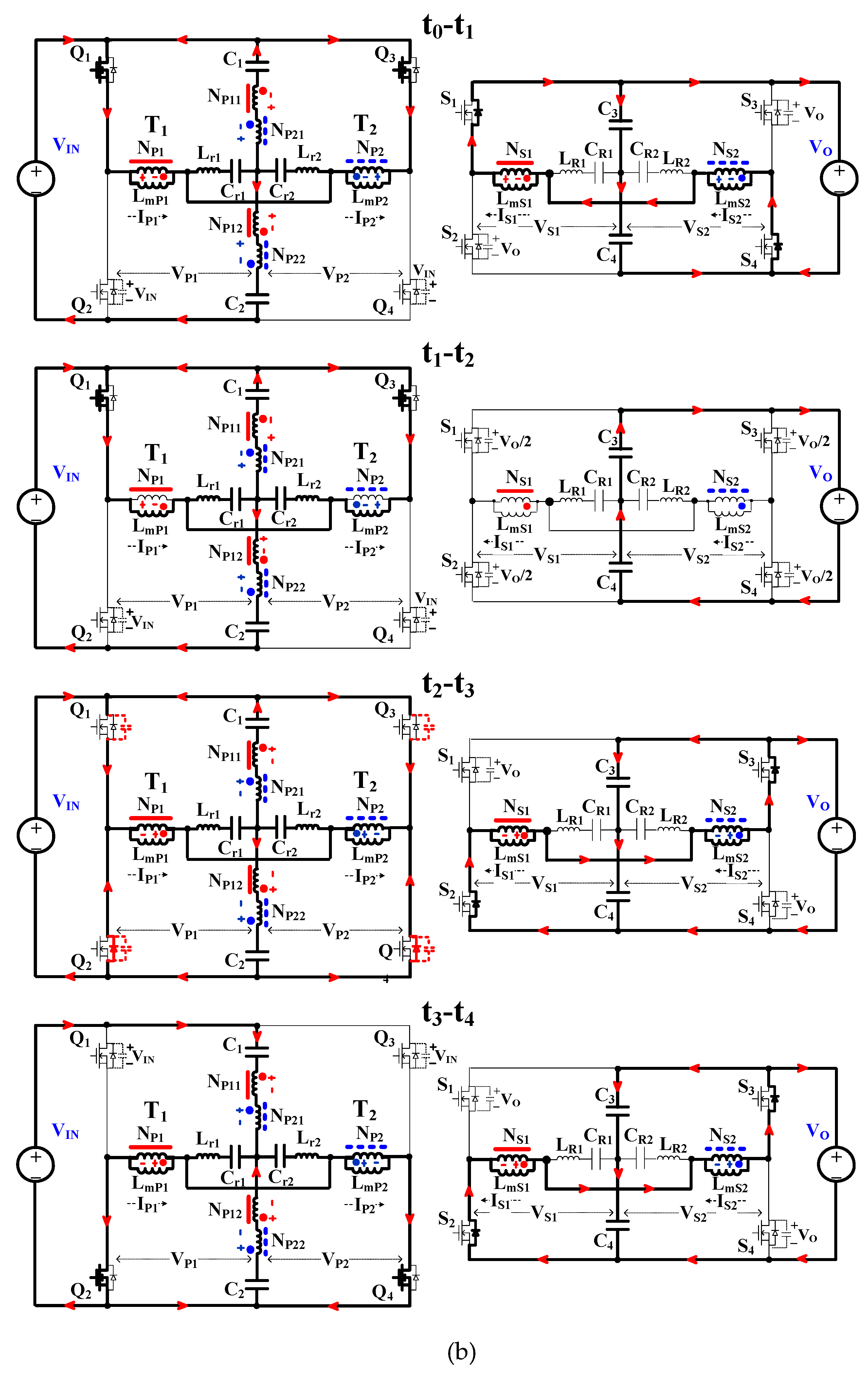
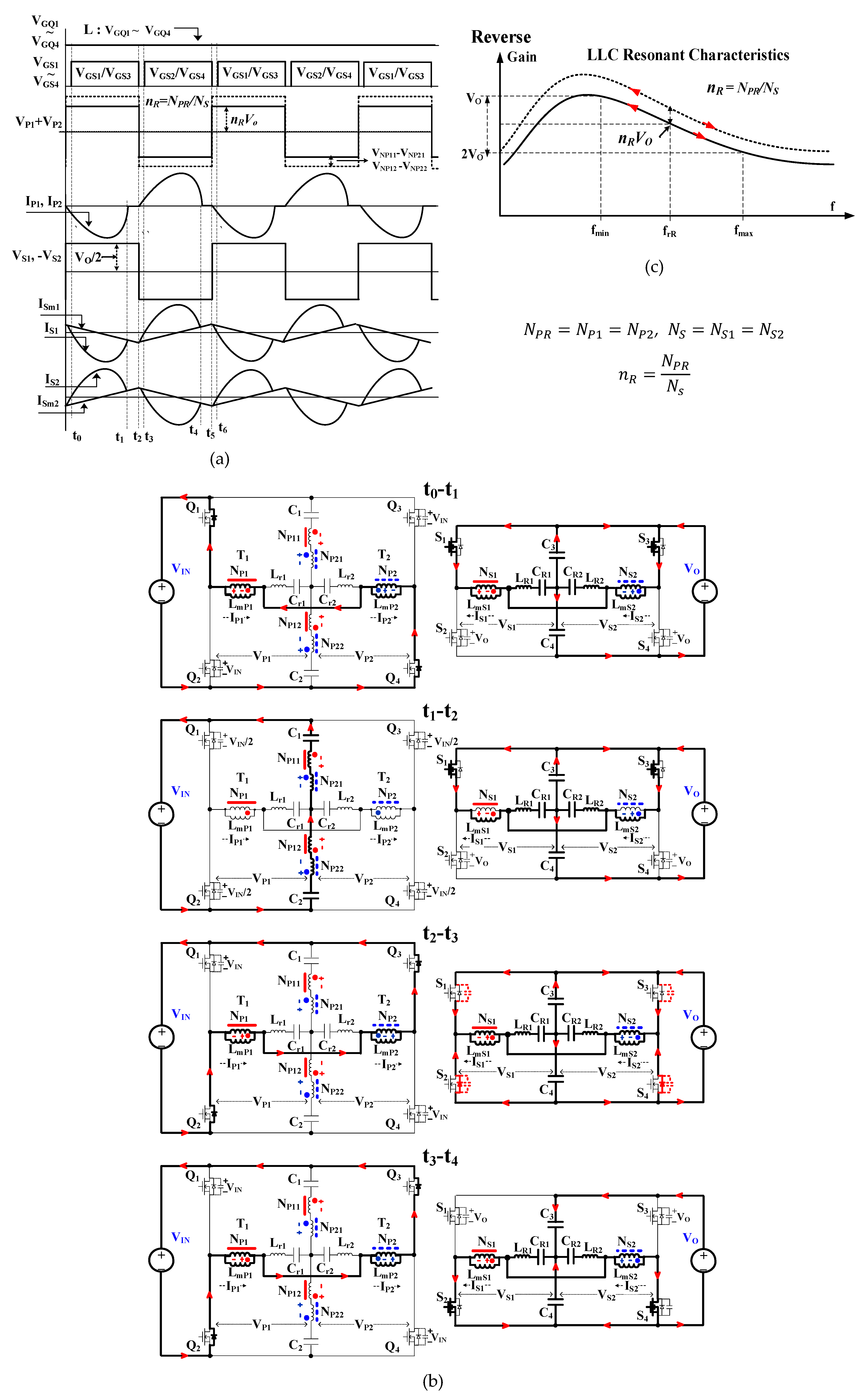
2.2. Reverse Operation Mode

The reverse operation mode is shown in Figure 4a,b. The secondary switches (S1/S3 and S2/S4) are simultaneously turned on and off with a 50% duty cycle. The anti-parallel diodes of the primary switches (Q1/Q3, Q2/Q4) are operated as rectifier diodes since the primary switches (Q1, Q2, Q3, Q4) are turned off. During the time interval t0–t1, when the secondary switches (S1/S3) are turned on with ZVS, half of the output voltage (Vo) is applied to each secondary resonant circuits, and in the reverse operation mode, as in the forward operation mode, the secondary resonant currents IS1(IS2) flow through the paths of the voltage divided capacitor (C3) → S1(S3) → secondary main windings NS1(NS2) → the resonant inductors LR1(LR2) and capacitors CR1(CR2), and back to the voltage divided capacitor (C3), respectively. Furthermore, the secondary resonant currents IS1(IS2) flow through the paths of the output voltage (VO) → S1(S3) → secondary windings NS1(NS2) → the resonant inductors LR1(LR2) and capacitors CR1(CR2) → the voltage divided capacitor (C4), and back to the output voltage (VO), respectively. If there is a difference in the resonant current (IS1, IS2) flowing in each secondary resonant circuit, the current flows through the secondary common connection line by the voltage difference charged in the resonant capacitors (CR1, CR2) to suppress the imbalance of the secondary resonant currents (IS1, IS2). At this point, the primary polarity of transformers (T1, T2) is changed by the secondary voltage applied to the secondary windings (NS1, NS2) of transformers, and the sum voltage (VP1 + VP2) of the primary windings (NP1, NP2) is transferred to the input side (VIN). As a result, the sum voltage of the auxiliary windings (NP11–NP21, NP12–NP22) connected to the primary resonance circuits is zero, which means that the primary resonant currents (IP1, IP2) do not flow through the primary resonant capacitors (Cr1, Cr2), but flow through the primary common connection line and anti-parallel diodes of the primary switching devises (Q2/Q3, Q1/Q4). Thus, in reverse operation mode, high LLC gain characteristics can be obtained without mutual coupling even though resonant capacitors (Cr1/Cr2, CR1/CR2) are used on the primary and secondary sides. Also, by using the primary auxiliary windings (NP11–NP21, NP12–NP22) of transformers in the resonant circuits, the transferred voltage to the primary is lowered by the turn-ratio (nR: NP1/NS1, NP2/NS2) during the reverse power transfer operation. This can easily control the gain voltage range according to the battery charging and discharging voltage in the forward and reverse power transfer operation. In the interval t1–t2, the resonant state ends, and only the secondary magnetizing currents (ISm1, ISm2) flow through the magnetizing inductance (LmS1, LmS2) of the transformers (T1, T2). When the secondary switches (S1/S3) are turned off at time t2, due to the secondary magnetizing currents of the transformers (T1, T2), the output parasitic capacitance of S1/S3 and S2/S4 are charged and discharged to the output voltage (VO) and zero voltage, respectively, during the dead time (t2–t3). During the dead time t2–t3, if the secondary switches (S2/S4) are turned on when the current is flowing in their anti-parallel diodes, S2 and S4 are operated with zero voltage switching.

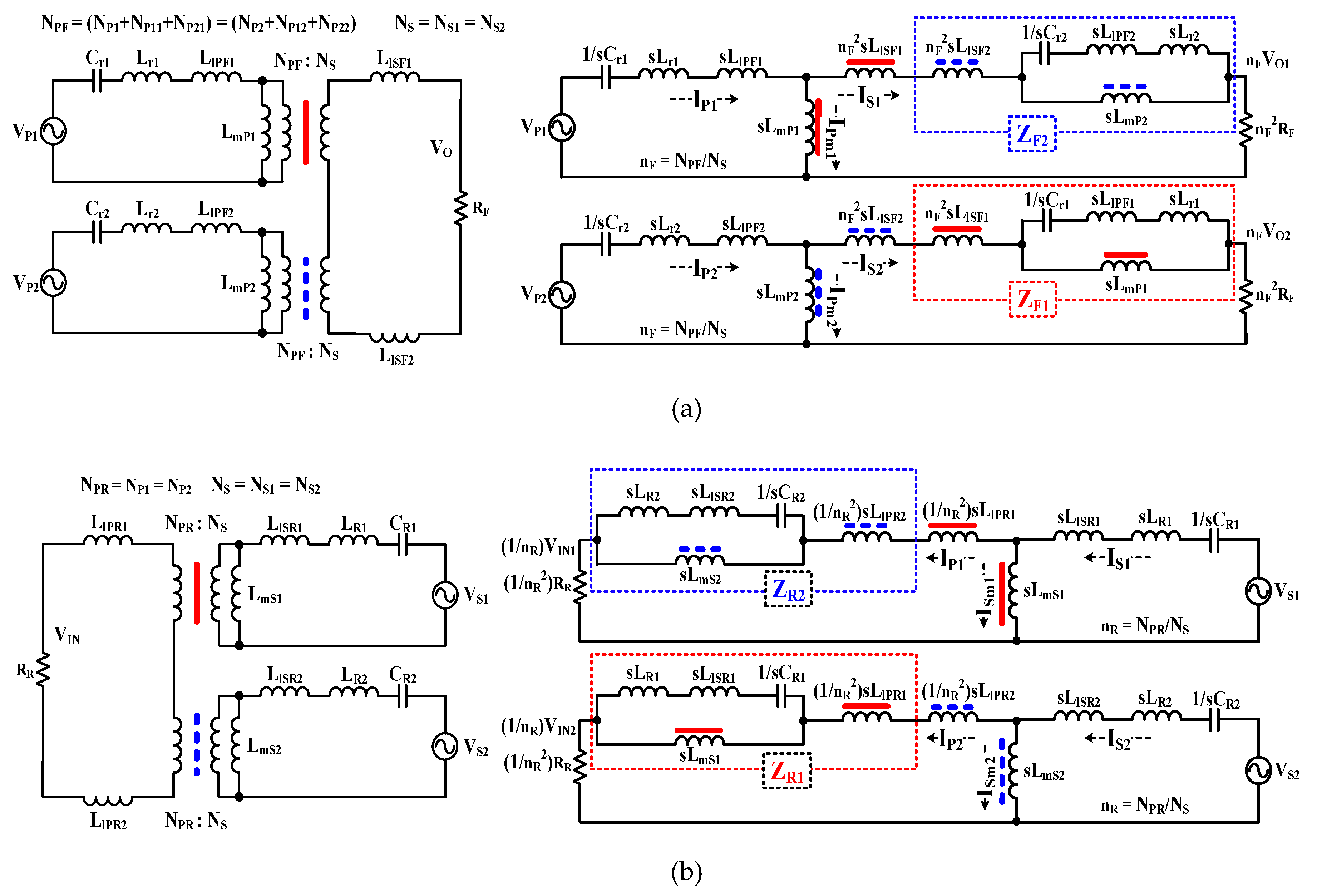
2.3. Equivalent Circuits of the Proposed Converter

In this section, voltage gain characteristics for both forward and reverse operation modes are discussed. To analyze the forward and reverse voltage gain characteristics, the converter can be simplified as T-shaped equivalent circuits since the proposed bidirectional LLC converter operates with the high gain characteristics of a conventional LLC resonant converter without the mutual coupling of resonant capacitors. Also, as the proposed bidirectional LLC resonant converter is operated by two resonant circuits in the forward and reverse operation modes, the converter’s gain characteristics can be obtained by the superposition principle considering the individual voltage sources (VP1/VP2, VS1/VS2) as shown in Figure 5a,b.
The converter’s voltage gain equations (GF, GR) expressed by the turn-ratio ( n F = N P F N s , n R = N P R N S ) and the parameters of transformers are shown as the sum of individual voltage gains (GF1 and GF2, GR1 and GR2) in the forward and reverse operation mode. Figure 5a shows the equivalent circuit considering the individual primary voltage sources (VP1, VP2) in the forward operating mode. The voltage gain characteristics (GF1) of the primary voltage source 1 (VP1) and load voltage ( n F VO1) can be shown as Equation (1). Also, the voltage gain characteristics (GF2) of the primary voltage source 2 (VP2) and load voltage ( n F VO2) can be shown as Equation (2). Therefore, the final voltage gain (GF) in the forward operation mode of the proposed converter is the sum of Equation (1) and Equation (2), as shown in Equation (3). In the forward operation mode, as shown in the equivalent circuits of Figure 5a, the equations related to the individual primary resonant impedances (ZF1, ZF2), and transformer parameters are shown below. Here, LmP1/LmP2 are the primary magnetizing inductance and LlPF1/LlPF2, LlSF1/LlSF2 are the primary and secondary leakage inductance, respectively, in the forward operation mode, and LeqF1/LeqF2 are the equivalent leakage inductance.
G F 1 =   n F V O 1 V P 1 = 1 2 [ n F 2 R F s L m P 1 C r 1 L m P 1 + n F 2 L l S F 1 n F 2 R F + Z F 2 s ( L m P 1 + n F 2 L l S F 1 ) { 1 + s 2 C r 1 ( L m P 1 + L l P F 1 + L r 1 ) } + ( 1 + s 2 C r 1 L e q F 1 ) ]
G F 2 =   n F V O 2 V P 2 = 1 2 [ n F 2 R F s L m P 2 C r 2 L m P 2 + n F 2 L l S F 2 n F 2 R F + Z F 1 s ( L m P 2 + n F 2 L l S F 2 ) { 1 + s 2 C r 2 ( L m P 2 + L l P F 2 + L r 2 ) } + ( 1 + s 2 C r 2 L e q F 2 ) ]
G F = G F 1 + G F 2 = n F V o V I N
where Z F 2 = s ( L m P 2 + n F 2 L l S F 2 )   1 + s 2 C r 2 L e q F 2 1 + s 2 C r 2 ( L m P 2 + L l P F 2 + L r 2 ) ; Z F 1 = s ( L m P 1 + n F 2 L l S F 1 )   1 + s 2 C r 1 L e q F 1 1 + s 2 C r 1 ( L m P 1 + L l P F 1 + L r 1 ) ; N P F = N P 1 + N P 11 + N P 21 = N P 2 + N P 12 + N P 22 ,     N S = N S 1 = N S 2 ; n F = N P F N S ; L e q F 1 = ( L l P F 1 + L r 1 ) + L m P 1 / / n F 2 L l S F 1 ; L e q F 2 = ( L l P F 2 + L r 2 ) + L m P 2 / / n F 2 L l S F 2 ;
Furthermore, the equivalent circuits considering the individual secondary voltage sources (VS1, VS2) in the reverse operation mode can be shown in Figure 5b. Moreover, the voltage gain characteristics (GR1, GR2) of the secondary voltage sources (VS1, VS2) and primary voltages (( 1 / n R )VIN1, ( 1 / n R )VIN2) can be found with Equation (4) and Equation (5). Therefore, the final voltage gain (GR) in the reverse operation mode of the proposed converter is the sum of Equation (4) and Equation (5), as shown in Equation (6). Here, LmS1/LmS2 and LlSR1/LlSR2 are the secondary magnetizing inductance and leakage inductance, and LlPR1/LlPR2 and LeqR1/LeqR2 are the primary leakage inductance and the equivalent leakage inductance in the reverse operation mode.
G R 1 =   V I N 1 n R V S 1 = 1 2 [ ( 1 / n R 2 ) R R s L m S 1 C R 1 L m S 1 + ( 1 / n R 2 ) L l P R 1 ( 1 / n R 2 ) R R + Z R 2 s ( L m S 1 + ( 1 / n R 2 ) L l P R 1 ) { 1 + s 2 C R 1 ( L m S 1 + L l S R 1 + L R 1 ) } + ( 1 + s 2 C R 1 L e q R 1 ) ]
G R 2 =   V I N 2 n R V S 2 = 1 2 [ ( 1 / n R 2 ) R R s L m S 2 C R 2 L m S 2 + ( 1 / n R 2 ) L l P R 2 ( 1 / n R 2 ) R R + Z R 1 s ( L m S 2 + ( 1 / n R 2 ) L l P R 2 ) { 1 + s 2 C R 2 ( L m S 2 + L l S R 2 + L R 2 ) } + ( 1 + s 2 C R 2 L e q R 2 ) ]
G R = G R 1 + G R 2 = V I N n R V o
where Z R 2 = s ( L m S 2 + ( 1 / n R 2 ) L l P R 2 )   1 + s 2 C R 2 L e q R 2 1 + s 2 C R 2 ( L m S 2 + L l S R 2 + L R 2 ) ; Z R 1 = s ( L m S 1 + ( 1 / n R 2 ) L l P R 1 )   1 + s 2 C R 1 L e q R 1 1 + s 2 C R 1 ( L m S 1 + L l S R 1 + L R 1 ) ; Z R 1 = s ( L m S 1 + ( 1 / n R 2 ) L l P R 1 )   1 + s 2 C R 1 L e q R 1 1 + s 2 C R 1 ( L m S 1 + L l S R 1 + L R 1 ) ; N P R = N P 1 = N P 2 ; N S = N S 1 = N S 2 ; n R = N P R N S ; L e q R 1 = ( L l S R 1 + L R 1 ) + L m S 1 / / ( 1 / n R 2 ) L l P R 1 ; L e q R 2 = ( L l S R 2 + L R 2 ) + L m S 2 / / ( 1 / n R 2 ) L l P R 2 .
Equation (7) and Equation (8) show the corner frequency (foF, foR) and resonant frequency (frF, frR) in the forward and reverse operation mode, respectively.
f o F = 1 2 π C r 1 ( L m P 1 + L l P F 1 + L r 1 ) = 1 2 π C r 2 ( L m P 2 + L l P F 2 + L r 2 ) ,     f r F = 1 2 π C r 1 L e q F 1 = 1 2 π C r 2 L e q F 2
f o R = 1 2 π C R 1 ( L m S 1 + L l S R 1 + L R 1 ) = 1 2 π C R 2 ( L m S 2 + L l S R 2 + L R 2 ) ,   f r R = 1 2 π C R 1 L e q R 1 = 1 2 π C R 2 L e q R 2
In the voltage gain characteristics (GF, GR) shown in Figure 6a and Figure 7a, the corner frequency (foF, foR) represents the frequency when the load in the forward and reverse operation mode are open (nF2RF = (1/nR2)RR = ). The frF and frR are the resonant frequency when the load in the forward and reverse operation mode are shorted (nF2RF = (1/nR2)RR = 0). The peaking at corner frequency (foF, foR) is generated due to the different values in the inductance of transformers (T1, T2). This peak will disappear when each transformer has the same inductance parameters.
To improve the gain characteristics of the forward and reverse operation based on voltage gain equations (GF, GR), the switching frequency and the transformer’s turn-ratio at the nominal voltage conditions of the battery must be set to operate in the vicinity of the resonant frequency (frF, frR). In this condition, primary auxiliary windings (NP11/NP12, NP21/NP22) used to adjust the gain characteristics have a very important role in achieving high voltage gain characteristics for the whole load range variation in both forward operation mode and reverse operation mode.

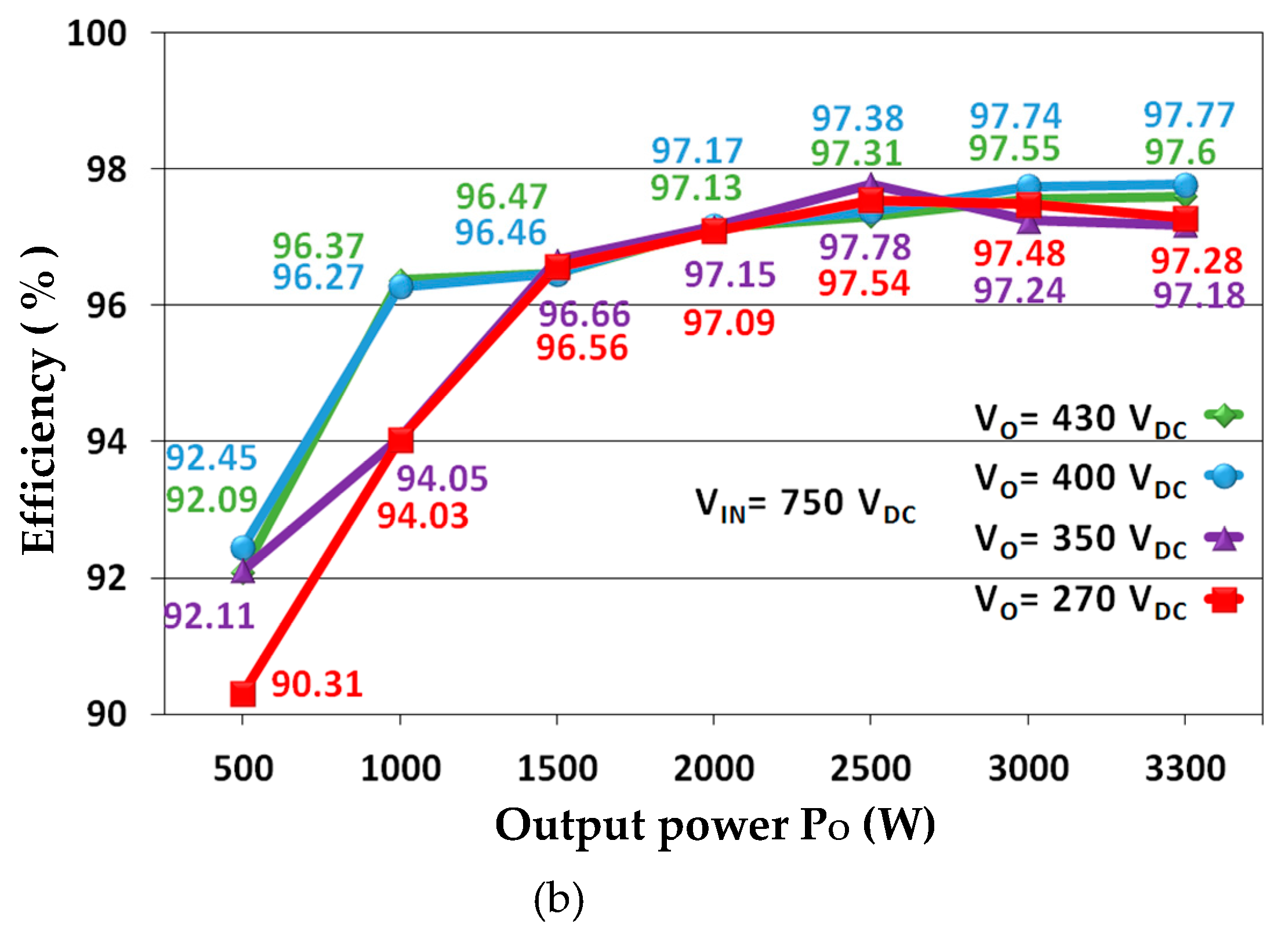
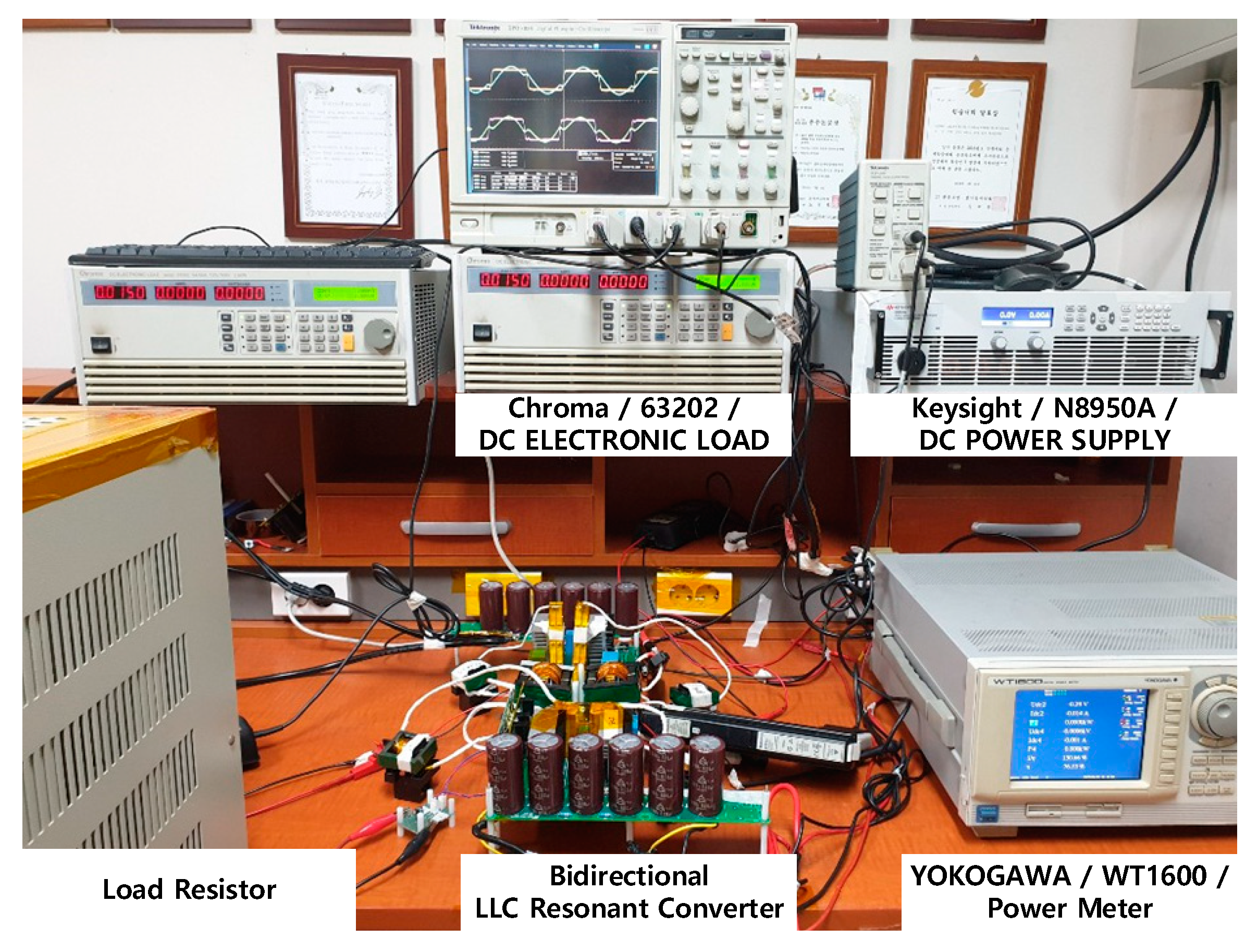
3. Experimental Results

In this paper, a 3.3 kW prototyped LLC resonant converter for bidirectional power conversion with a 750 VDC input voltage and an output voltage range of 270–430 VDC was built and tested to verify the validity of the proposed converter. The experimental conditions and specifications are shown in Table 1. Note that T represents the number of turns.
Figure 6 and Figure 7 show the results of our experiment, describing the waveforms of each circuit component in the forward and reverse operation mode, respectively. The experimental waveforms of the primary terminal voltage/current (VP1, IP1) and the secondary terminal voltage/current (VS1, IS1) are given for a capacity of 3.3 kW with an input voltage (750 VDC) and output voltage (270 VDC/350 VDC/430 VDC), in the forward and reverse operation, respectively.
The results of the experiment and simulation (Math-Cad) in both the forward and reverse operations confirmed that the proposed bidirectional LLC resonant converter for wide output voltage control (270–430 VDC) operates with LLC resonant gain characteristics in the frequency control range of 220 kHz to 600 kHz. Therefore, we proved that the proposed bidirectional LLC resonant converter can operate with the same high gain characteristics as a conventional LLC resonant converter without the mutual coupling of resonant capacitors.
Figure 8a,b show the efficiency characteristics of the proposed bidirectional LLC resonant converter in the forward and reverse operation modes, respectively. In the forward operation mode, as shown in Figure 8a, the efficiency at maximum power (3.3 kW) with an input voltage of 750 VDC and output voltage of 350 VDC was 98.48%, and the maximum efficiency was 98.75% at an input voltage of 350 VDC and power capacity of 2.5 kW because the switching operation was close to the resonant frequency (frF: 296 kHz). In the reverse operation mode, the maximum efficiency with an input voltage of 750 VDC and output voltage of 350 VDC, 2.5 kW was 97.78%, as shown in Figure 8b.
The experimental setup for the laboratory prototype 3.3 kW bidirectional LLC resonant converter is shown in Figure 9.

4. Discussion

A bidirectional DC–DC converter with high power density and efficiency has been proposed for on-board chargers (OBC) for EVs and as a DC micro-grid for an electrical storage system. As shown in Figure 1, the CLLC resonant converter has recently been developed for the electric vehicle OBC, but to improve the gain characteristics below the resonant frequency is challenging, as mentioned above. To overcome these problems, a topology comprised of a Power Factor Correction (PFC) AC–DC converter operating with variable DC-link voltage and a CLLC resonant DC–DC converter operating with fixed switching frequency is considered as key for various applications [4]. However, PFC AC–DC converters are hard-switching, which limits the switching frequency for integration and increases the voltage rating of switching devices and DC link capacitors according to the increased DC link voltage.
To overcome these limitations, we show that the proposed bidirectional LLC resonant converter could be implemented with a wide output voltage range.

5. Conclusions

In this paper, a simple scheme for a bidirectional LLC resonant DC–DC converter using the primary auxiliary windings and two resonant circuits was proposed, and this shows the LLC resonant characteristics for both forward and reverse directional operations. Experiments with a fabricated 3.3 kW prototype were conducted to evaluate the proposed bidirectional LLC resonant converter. The experimental results show that the proposed topology is a viable solution for the design of bidirectional DC–DC converters.

6. Patents

E.S Kim. Bidirectional LLC Resonant Converter. Patent-pending (No: 10-2019-0011426), South Korea, 2019.1.29.

Author Contributions

The authors contributed to the paper as follows: Study conception and idea, E.-S.K.; Experiment and results, J.-S.O.; Draft manuscript preparation, E.-S.K.

Funding

This work was supported by the National Research Foundation of Korea (NRF) grant funded by the Korean Government (MSIT) (No. 2018008925).

Conflicts of Interest

The authors declare no conflict of interest.

References

  1. Wang, K.; Zhu, L.; Qu, D.; Odendaal, H.; Lai, J.; Lee, F.C. Design implementation and experimental results of bidirectional full-bridge dc/dc converter with unified soft-switching scheme and soft-starting capability. IEEE PESC 2000, 2, 1058–1063. [Google Scholar]
  2. Krismer, F.; Biela, J.; Kolar, J.W. A Comparative Evaluation of Isolated Bi-directional DC/DC Converters with Wide Input and Output Voltage Range. IEEE IAS 2005, 1, 599–606. [Google Scholar]
  3. He, P.; Khaligh, A. Comprehensive Analyses and Comparison of 1 kW Isolated DC–DC Converters for Bidirectional EV Charging Systems. IEEE Trans. Transp. Electrif. 2017, 3, 147–156. [Google Scholar] [CrossRef]
  4. Liu, Z.; Li, B.; Lee, F.C.; Li, Q. Design of CRM AC/DC Converter for Very High-Frequency High-Density WBG-Based 6.6 kW Bidirectional On-Board Battery Charge. In Proceedings of the 2016 IEEE Energy Conversion Congress and Exposition (ECCE), Milwaukee, WI, USA, 18–22 September 2016. [Google Scholar]
  5. Chen, W.; Rong, P.; Lu, Z. Snubberless Bidirectional DC–-DC Converter With New CLLC Resonant Tank Featuring Minimized Switching Loss. IEEE Trans. Ind. Electron. 2010, 57, 3075–3086. [Google Scholar] [CrossRef]
  6. Wei, C.; Shao, J.; Agrawal, B.; Zhu, D.; Xie, H. New Surface Mount SiC MOSFETs Enable High Efficiency High Power Density Bi-directional On-Board Charger with Flexible DC-link Voltage; IEEE APEC: Anaheim, CA, USA, 2019. [Google Scholar]
  7. Lee, J.Y.; Jeong, Y.S.; Han, B.M. A Two-Stage Isolated/Bidirectional DC/DC Converter with Current Ripple Reduction Technique. IEEE Trans. Ind. Electron. 2012, 59, 644–646. [Google Scholar] [CrossRef]
  8. Kim, E.S. Bidirectional LLC Resonant Converter. Patent pending (10-2019-0011426), 29 January 2019. [Google Scholar]
Figure 1. Two-stage bidirectional converter and gain characteristics: (a) Conventional two-stage bidirectional converter; (b) LLC gain characteristics; (c) CLLC gain characteristics.
Energies 12 04692 g001aEnergies 12 04692 g001b
Figure 2. Proposed bidirectional LLC resonant DC–DC converters: (a) Proposed converter 1; (b) Proposed converter 2; (c) Proposed converter 3.
Energies 12 04692 g002aEnergies 12 04692 g002b
Figure 3. Operating waveforms and operating modes in the forward operation mode: (a) Operating waveforms; (b) Operating modes; (c) Gain characteristics considering the turn-ratio (nF).
Energies 12 04692 g003aEnergies 12 04692 g003b
Figure 4. Operating waveforms and operating modes in the reverse operation mode: (a) Operating waveforms; (b) Operating modes; (c) Gain characteristics considering the turn-ratio (nR).
Energies 12 04692 g004
Figure 5. Equivalent circuits considering the individual voltage sources (VP1/VP2, VS1/VS2): (a) Equivalent circuit in the forward operation mode; (b) Equivalent circuit in the reverse operation mode.
Energies 12 04692 g005
Figure 6. Experimental waveforms and voltage gain characteristics in the forward operation mode.
Energies 12 04692 g006
Figure 7. Experimental waveforms and voltage gain characteristics in the reverse operation mode.
Energies 12 04692 g007
Figure 8. Efficiency characteristics in forward and reverse operating conditions: (a) Forward operation mode; (b) Reverse operation mode.
Energies 12 04692 g008aEnergies 12 04692 g008b
Figure 9. Photograph of the converter experiment.
Energies 12 04692 g009
Table 1. Major ratings and parameters of the proposed converter.
Specification/ParametersValues
Input voltage (VIN)750 VDC
Output voltage (VO)/Power rating (PO)270 VDC–430 VDC/3.3 kW
Switching Devices (Q1–Q4)UJ3C120040K3S(1200 V, 65 A, RDS: 35 mΩ, SiC)
Switching Devices (S1–S4)UJ3C065030K3S(650 V, 85 A, RDS: 27 mΩ, SiC)
Resonant Capacitors [(Cr1,Cr2)/CR1,CR2)]10.5 nF/56 nF
Resonant Inductors [(Lr1,Lr2)/LR1,LR2)]22.1 uH/4 uH
Resonant Frequency [frF/frR: Forward/Reverse]
Switching Frequency Range (fs)
296.3 kHz/303.7 kHz
220 kHz–600 kHz
Forward operation mode
Primary self-inductance
[T1/T2: LlPF1 + LmP1/LlPF2 + LmP2]
61.4 uH/61.1 uH
Secondary self-inductance
[T1/T2: LlSF1 +   ( 1/ n F 2 ) LmP1/LlSF2 + ( 1/ n F 2 ) LmP2]
11.73 uH/11.65 uH
Primary magnetizing Inductance
[T1/T2: LmP1/LmP2]
57.65 uH/57.28 uH
Turn-ratio [ N PF / N S = n F ]2.25 [18 T(14 T + 2 T + 2 T)/8 T]
Reverse operation mode
Primary self-inductance
[T1/T2:LlPR1 +   n R 2 LmS1/LlPR2 + n R 2 LmS2]
35.06 uH/35.28 uH
Secondary self-inductance
[T1/T2: LlSR1+LmS1/LlSR2 + LmS2]
11.73 uH/11.65 uH
Secondary magnetizing Inductance
[T1/T2: LmS1/LmS2]
11.04 uH/11.13 uH
Turn-ratio [ N PR / N S = n R ]1.75 [14 T/8 T]

