Article

Switching Characteristics Optimization of Two-Phase Interleaved Bidirectional DC/DC for Electric Vehicles

School of Mechanical and Automotive Engineering, South China University of Technology, Guangzhou 510641, China
*
Author to whom correspondence should be addressed.
Energies 2019, 12(3), 378; https://doi.org/10.3390/en12030378
Submission received: 24 December 2018 / Revised: 20 January 2019 / Accepted: 21 January 2019 / Published: 24 January 2019
(This article belongs to the Section E: Electric Vehicles)

Abstract

:
In electric vehicles (EVs), bidirectional DC/DC(Bi-DC/DC) is installed between the battery pack and the DC bus to step up the voltage. In the process of mode switching under step signal, the Bi-DC/DC will be affected by a large current inrush which threatens the safety of the circuit. In this paper, a Bi-DC/DC mode switching method based on the optimized Bézier curve is proposed. The Boost and Buck modes can be switched based on the proposed method with fast and non-overshoot switching performance. The experimental results show that the mode switching can be finished in 4 ms without overshoot based on the optimal switching curve.

1. Introduction

As a key component of electric vehicles (EVs), bidirectional DC/DC (Bi-DC/DC) plays an important role in DC power conversion, allowing current can flow in two directions. The current flows in the forward direction during the driving process, while it flows in the reverse direction during the energy recovery process. Bi-DC/DC with high power and high efficiency is needed in the application of EVs [1,2,3,4,5]. Among all kinds of Bi-DC/DC topologies, the interleaved structure [6,7,8,9,10] which has the advantage of low output ripple is widely adopted. Urciuoli et al. studied the Bi-DC/DC with interleaved topology and designed a 90 kW prototype which showed a low ripple rate and a high-power density [11]. Thounthong et al. developed a Boost DC/DC with two-phase interleaved topology for fuel cells, which has low current ripple [12,13]. Xu et al. also designed a Bi-DC/DC with two-phase interleaved topology, which has greatly reduced the volume and weight compared to the traditional Bi-DC/DC [14,15].
When Bi-DC/DC works at start-up or mode switching, the dynamic characteristics of the system change sharply. Meanwhile, the abrupt signal will make the system more unstable or generate a large current surge. In addition, when the switching process is not properly controlled, the device will be damaged. A soft start as a traditional control method is often used to avoid current surge, but it will slow down the process of mode switching. However, the Buck and Boost modes usually switch frequently when the EV is running. In order to improve the performance of the system, faster response of mode switching is required to satisfy the power requirements of the vehicle. Therefore, it is necessary to study the mode switching characteristics and propose a better control method. Lai et al. [16] proposed a CMOS-compatible digital soft-start circuit, which could eliminate the inrush current and voltage overshoots without external soft-start capacitor. Zhou et al. [17] developed an AC coupled feedback circuit to accelerate the transient response of the DC/DC. C. Zhao et al [18] proposed a start-up method which controlled the process of mode switching in three stages for three-port converter: Buck mode control was firstly used, followed by Boost mode control, and finally converted to phase-shift control. Ryota Kondo et al. [19] proposed a new driving method for DC/DC, which synchronized one leg of each converter connected to both sides of the isolation transformer. And the switching time of charging and discharging is 7.6 ms under this control method.
In this paper, a novel DC/DC mode switching method based on the optimal Bézier curve is proposed. The Boost and Buck modes can be switched based on the proposed method with fast and non-overshoot switching performance. This paper is organized as follows: the mechanism of the Two-phase interleaved Bi-DC/DC, as well as the control method in each operating mode will be given in Section 2. Then the model of the Bi-DC/DC and the optimal switching method will be proposed in Section 3. Finally, experimental verification using a fabricated prototype will be presented in Section 4.

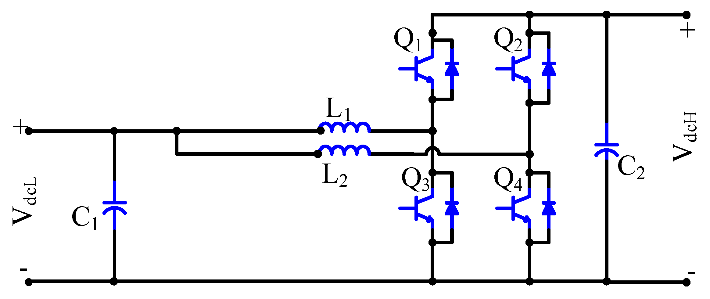
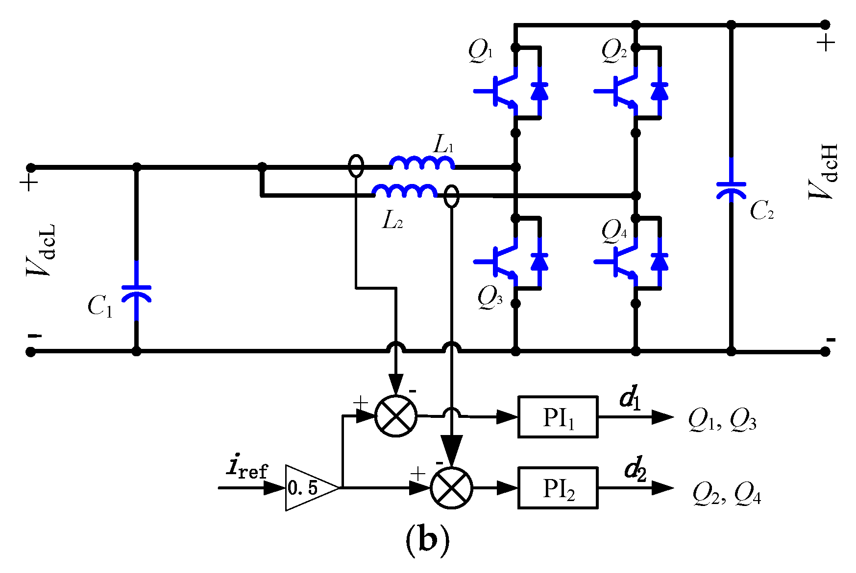
2. Modeling and Control of Two-Phase Interleaved Bi-DC/DC

Figure 1 shows the schematic illustration of Bi-DC/DC, which consists of four IGBTs: Q1, Q2, Q3 and Q4; two inductors L1 and L2; two DC filter capacitors C1 and C2. Where, VdcL is low-side voltage that connected to the low-voltage DC power source, VdcH is high-side voltage and it is connected to the high-voltage DC power source.
In Buck mode, IGBTs Q1 and Q2 are used as primary switches, which alternately are switched on or off by frequency f, and IGBTs Q3 and Q4 are turned off. When Q1 or Q2 is turned on, the current flows from high-voltage side to low-voltage side. When Q1 or Q2 is switched off, the inductor current flows through the free-wheeling diode of Q3 and Q4. While in Boost mode, the power flows from low-voltage side to high-voltage side, and Q1 and Q2 are turned off, and Q3 and Q4 as primary switches are alternately switched on or off by frequency f. When Q3 or Q4 is switched on, the current of the inductor increases. Otherwise, the current of the inductor flows through the free-wheeling diode of Q1 and Q2 when Q3 or Q4 is switched off. The Buck and Boost conversions exhibit a duality property. Whether in Buck or Boost conversion, the inductor L1 stores energy when Q1 or Q3 is turned on, and inductor L2 stores energy when Q2 or Q4 is turned on.

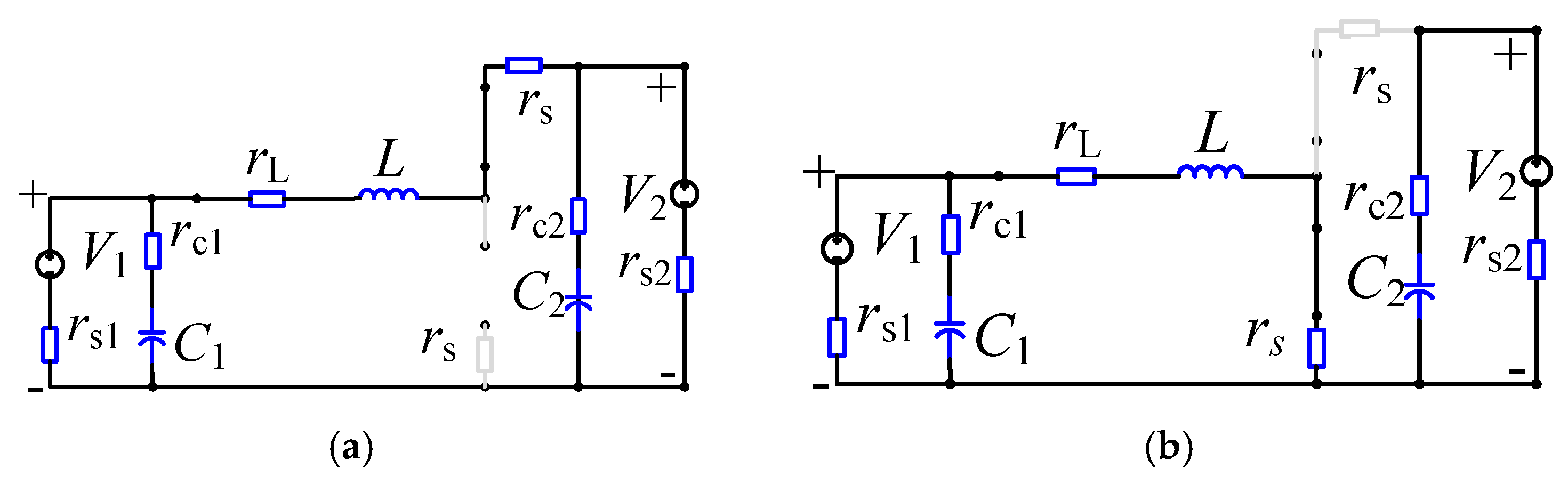
2.1. Modeling of the Bi-DC/DC

For both Boost mode and Buck mode, the IGBT in the two parallel branches drives PWM signal which are 180° out of phase in order to reduce the ripple of output current. It needs to separately control the two branches to ensure the balance of current. Since the two branches are symmetrical, it can be simplified to analyze one branch and design the control strategy separately, and finally apply the control strategy to another branch by delaying the switch with 180°.
When the two ends of the Bi-DC/DC are connected to different power supplies V 1 and V 2 , it works in inductor continuous conduction mode (CCM). At this time, the two operating states under Buck mode are shown in Figure 2. Figure 2a is the working state in which the switch is turned on, and Figure 2b is the working state in which the switch is turned off. The operating states of Boost mode is opposite to the Buck mode.
The state variable of the system can be defined as follows: x ( t ) : [ i L ( t ) , v c 1 ( t ) , v c 2 ( t ) ] , where i L ( t ) is inductor current, v c 1 ( t ) is voltage of capacitor C 1 , v c 2 ( t ) is voltage of capacitor C 2 . The input variable of the system can be defined as follows: u ( t ) : ( V 1 , V 2 ) . According to the equivalent circuit of Figure 2a, the coefficient matrix of the state equation can be calculated by Equation (1):
A 1 = [ r cLs 1 r c 1 s 1 L r s 1 r c 1 s 1 L 0 r s 1 r c 1 s 1 C 1 1 r c 1 s 1 C 1 0 0 0 1 r c 2 s 2 C 2 ] ,   B 1 = [ r c 1 r c 1 s 1 L 0 1 r c 1 s 1 C 1 0 0 1 r c 2 s 2 C 2 ]
where r cLs 1 = r c 1 r L + r c 1 r s + r c 1 r s 1 + r s 1 r L + r s 1 r s , r c 1 s 1 = r c 1 + r s 1 , r c 2 s 2 = r c 2 + r s 2 .
According to the equivalent circuit of Figure 2b, the coefficient matrix of the state equation can be derived as:
A 2 = [ r L s 1 s 2 L + r 2 s 1 r c 1 s 1 L + r 2 s 2 r c 2 s 2 L r s 1 r c 1 s 1 L r s 2 r c 2 s 2 L r s 1 r c 1 s 1 C 1 1 r c 1 s 1 C 1 0 r s 2 r c 2 s 2 C 2 0 1 r c 2 s 2 C 2 ] ,   B 2 = [ 1 L r s 1 r c 1 s 1 L r s 2 r c 2 s 2 L 1 L 1 r c 1 s 1 C 1 0 0 1 r c 2 s 2 C 2 ]
where, r L s 1 s 2 = r L + r s 1 + r s 2 .
In a switching cycle T s , the duty cycle of each state is d n which satisfies n = 1 2 d n = 1 . The duration of each state can be obtained as d n T s . By averaging the two states mentioned above, the average equation coefficient matrix of the state space can be derived as Equation (3):
A = n = 1 2 d n A n ,   B = B = 1 2 d n B n
where, n = 1, 2. According to the average equation of the state space, the transfer function, from the state variable to the duty cycle can be calculated as:
G xd = ( S I A ) 1 ( A x b 0 + B u b 0 ) d
where d is duty cycle. Let d 1 = d and d 2 = 1 d in Buck mode, d 2 = d and d 1 = 1 d in Boost mode in Equation (3). x b 0 means state variable of balance point. u b 0 means input quantity of balance point. Based on the transfer function in Equation (4), the system regulator of Bi-DC/DC mode G c ( s ) can be designed.

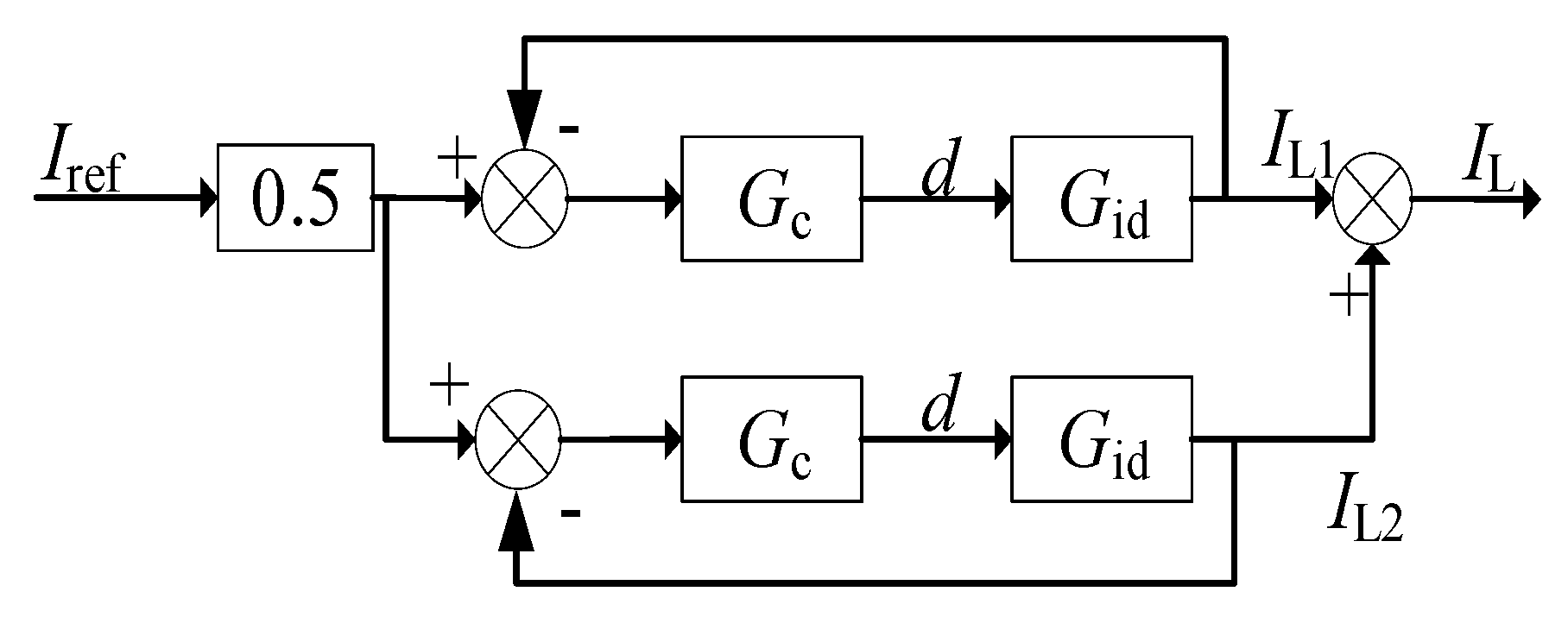
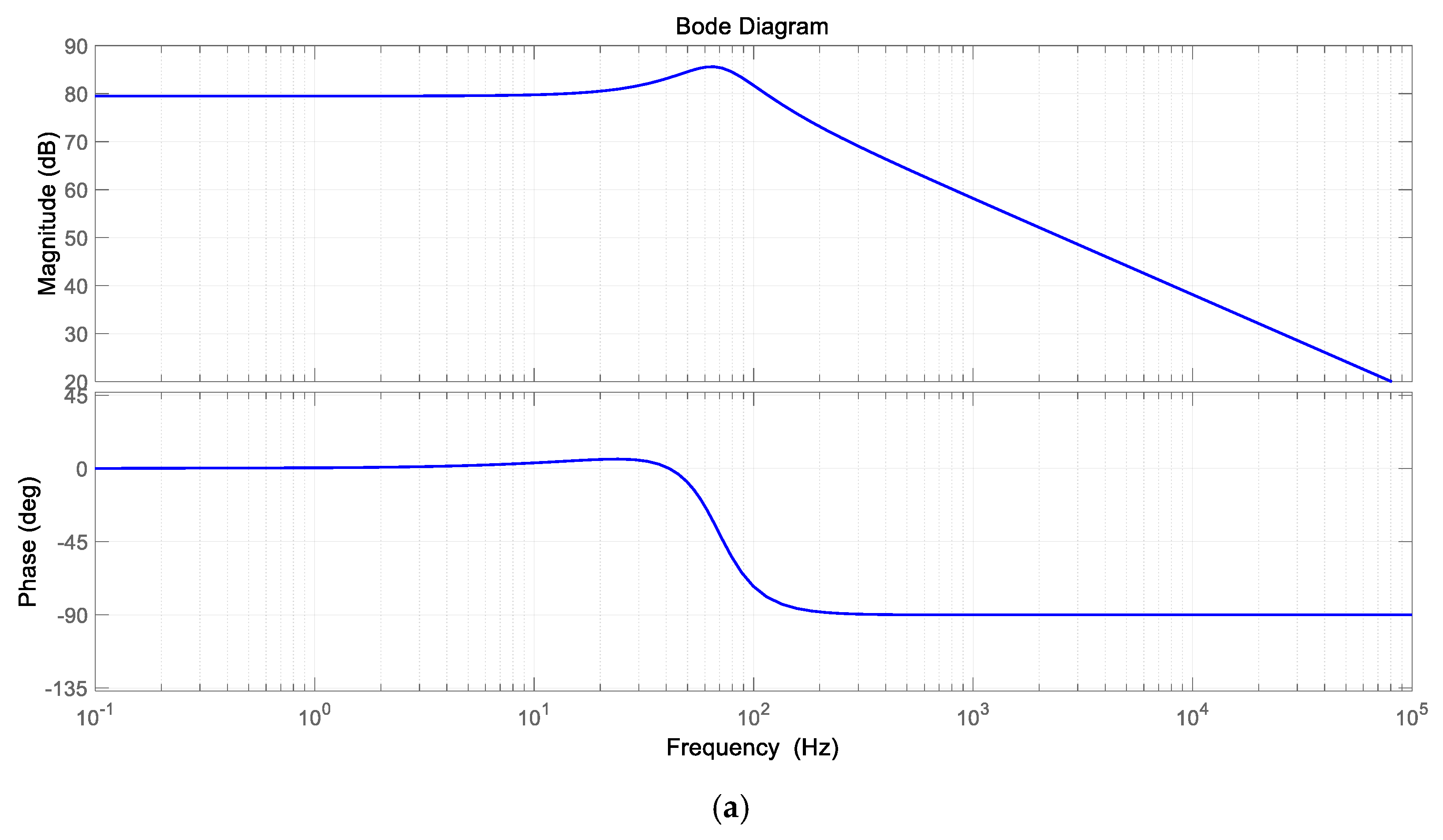
2.2. The Controller Design of the Bi-DC/DC

Assume that the transfer function of the system is G(s), input signal is R(s), output signal is C(s). During the process of each mode switching, it is necessary to ensure the smoothness and the rapidity of output signal, i.e., a small overshoot and a fast switching time. The current loop is used to control the Bi-DC/DC, since one end is connected to the battery pack and the other end is connected to the supercapacitor pack in the practical application. The transfer function from duty cycle d to inductor current is Gid(s), and the transfer function of regulator is Gc(s). The system structure is shown in Figure 3.
The closed loop transfer function of the system is shown in Equation (5):
G ( s ) = G c ( s ) G id ( s ) 1 + G c ( s ) G id ( s )
According to the Equation (5), it only needs to derive the transfer function Gid(s) of the single branch.
For the Bi-DC/DC designed in this paper, DC high-end voltage V d c H is 350 V, DC low-end voltage V d c L is 220 V, the inductance is 69 μF, the capacitance is 9400 μF, and the initial resistance of the DC high end is 320 mΩ. The initial current before switching is set to −175 A, the steady-state current is 175 A.
The PI controller is used as the regulator of the system, and its transfer function is shown in Equation (6):
G c ( s ) = k p + k i s
where, kp is the proportionality coefficient, ki is the integral coefficient.
Based on the model of the system illustrated in Equation (4), the parameters of the PI regulator can be obtained easily by the “sisotool” toolbox of MATLAB. According to reported literature [20], the PI controller must satisfy the following criteria: phase margin ≥45° and crossover frequency ≥198 Hz (3 times higher than the resonant frequency). Using the “sisotool”, PI controller parameters of the system shown in Figure 4a are: kp is 0.00097, and ki is 0.3458. The phase margin of the system is 63°, and the crossover frequency is 319 Hz.

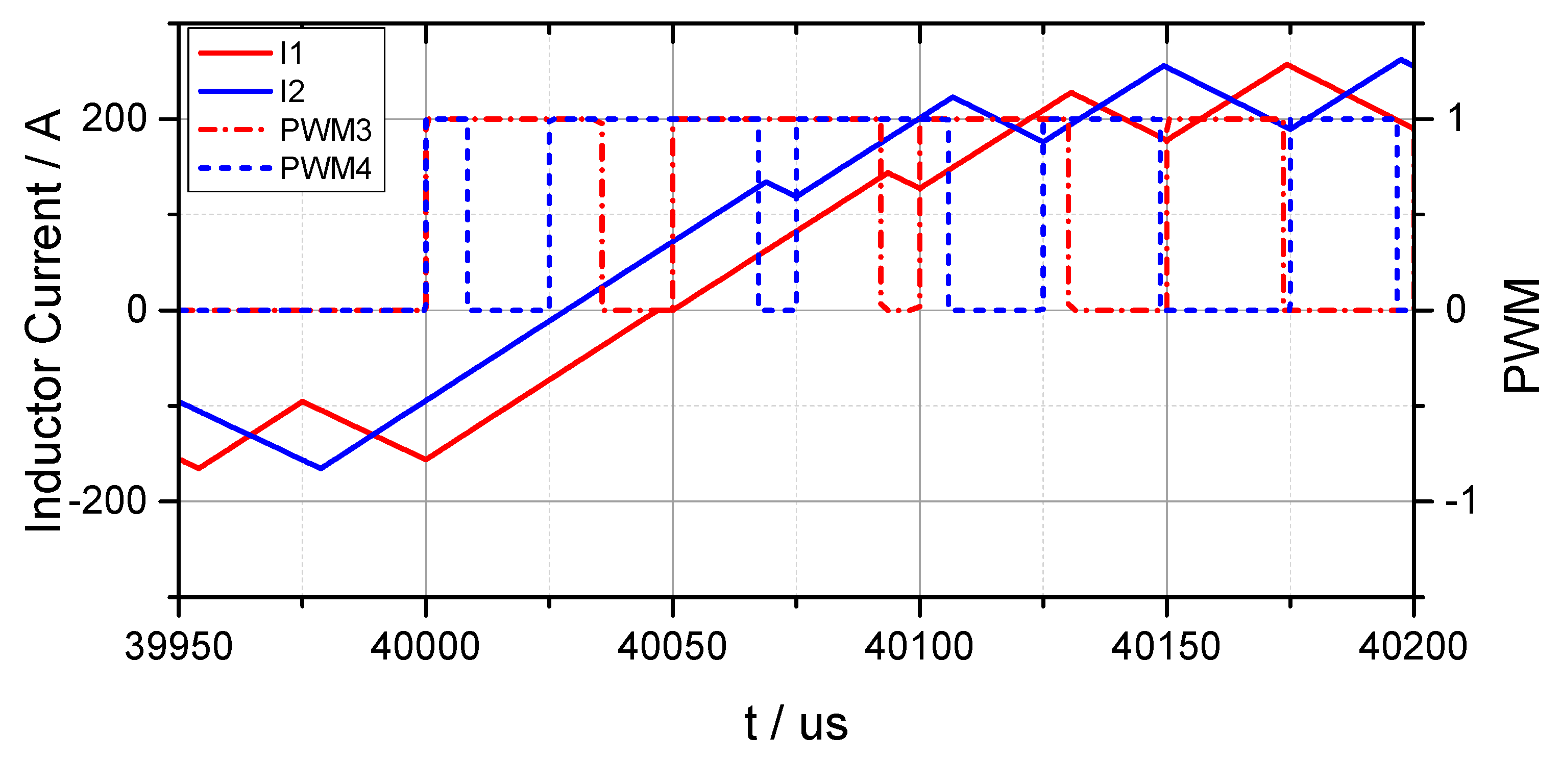
3. Optimizing of the Mode Switching

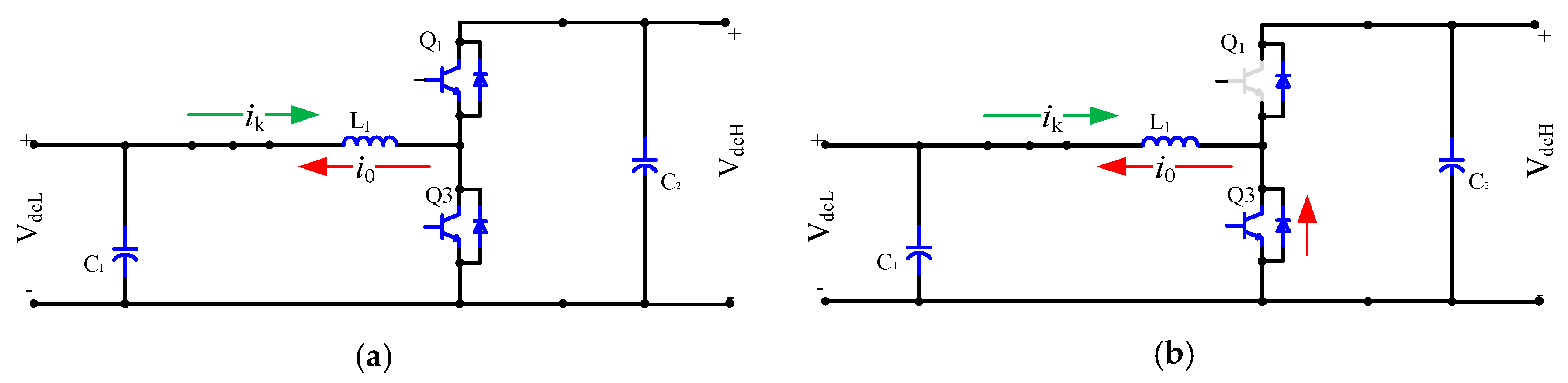
3.1. The Switching Characteristics of Bi-DC/DC

Since the Buck and Boost modes of Bi-DC/DC will alternately switch frequently, the characteristics of the switching process must be considered. In order to simplify the dynamic characteristics of the switching process, one branch of the interleaved Bi-DC/DC is used for further research.
As shown in Figure 5a, when Bi-DC/DC is in normal operation, the current in Buck mode flows from the high voltage side to the low voltage side, as indicated by the red arrow in the figure. By contrast, the current in Boost mode flows from the low voltage side to the high voltage side.
Taking Buck mode to Boost mode as an example, when the designed Bi-DC/DC works in CCM mode, the whole switching process will undergo the following steps:
(1)
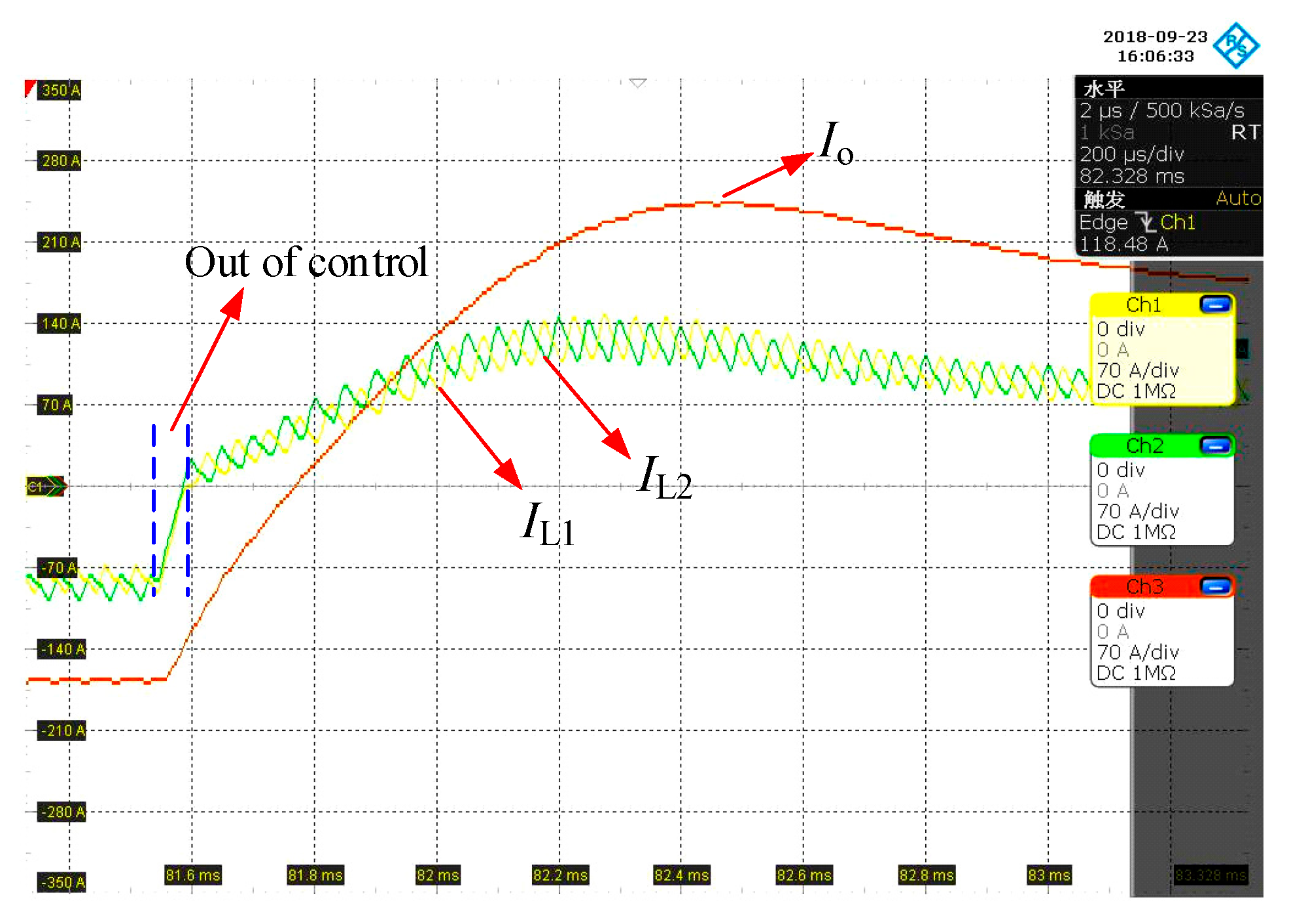
When mode switching starts, the Q1 is turned off and the Q3 is operated in the high frequency switching mode. The initial inductor current (i0) does not suddenly change its direction, so the current will still flow in the direction of the red arrow (Figure 5b);
(2)
In the second step, the initial current will gradually decrease from i0 to 0. During this period, whether Q3 is turned on or turned off, the current will flow in the direction of the red arrow and gradually decrease. This means that the system is out of control during this period and it is impossible to control the inductor current;
(3)
After the inductor current is reduced to zero, the system switches to Boost mode. Then the output voltage and current can be controlled by adjusting the duty cycle of Q3, and the switching from Buck mode to Boost mode is successfully completed.
Then, MATLAB/Simulink is utilized to simulate the switching characteristics of Bi-DC/DC from Buck mode to Boost mode. The current of the two inductors and the control signals of the two IGBTs are shown in Figure 6.
During mode switching, current surges are caused by two factors. Firstly, the mode switching process generates a large signal disturbance. Thus, the designed controller with small signal model cannot accurately control the system during the switching process. Secondly, the inductor current is uncontrollable during a period after the mode switching starts. Therefore, the controller will accumulate larger errors, which subsequently lead to larger overshoot. As shown in Figure 6, the solid red line and blue line represent the current waveform of the inductor L1 and L2, respectively; the red dotted line is the PWM signal to control Q3; while the blue dotted line is the PWM signal to control Q4. The mode switching of Bi-DC/DC starts at 40,000 μs.
As shown in Figure 6, the inductor current is uncontrollable at the beginning of the switching. Therefore, during the initial switching cycles, the inductor current does not reach the reference value, and the controller increases the duty cycle, resulting in a higher current overshoot.

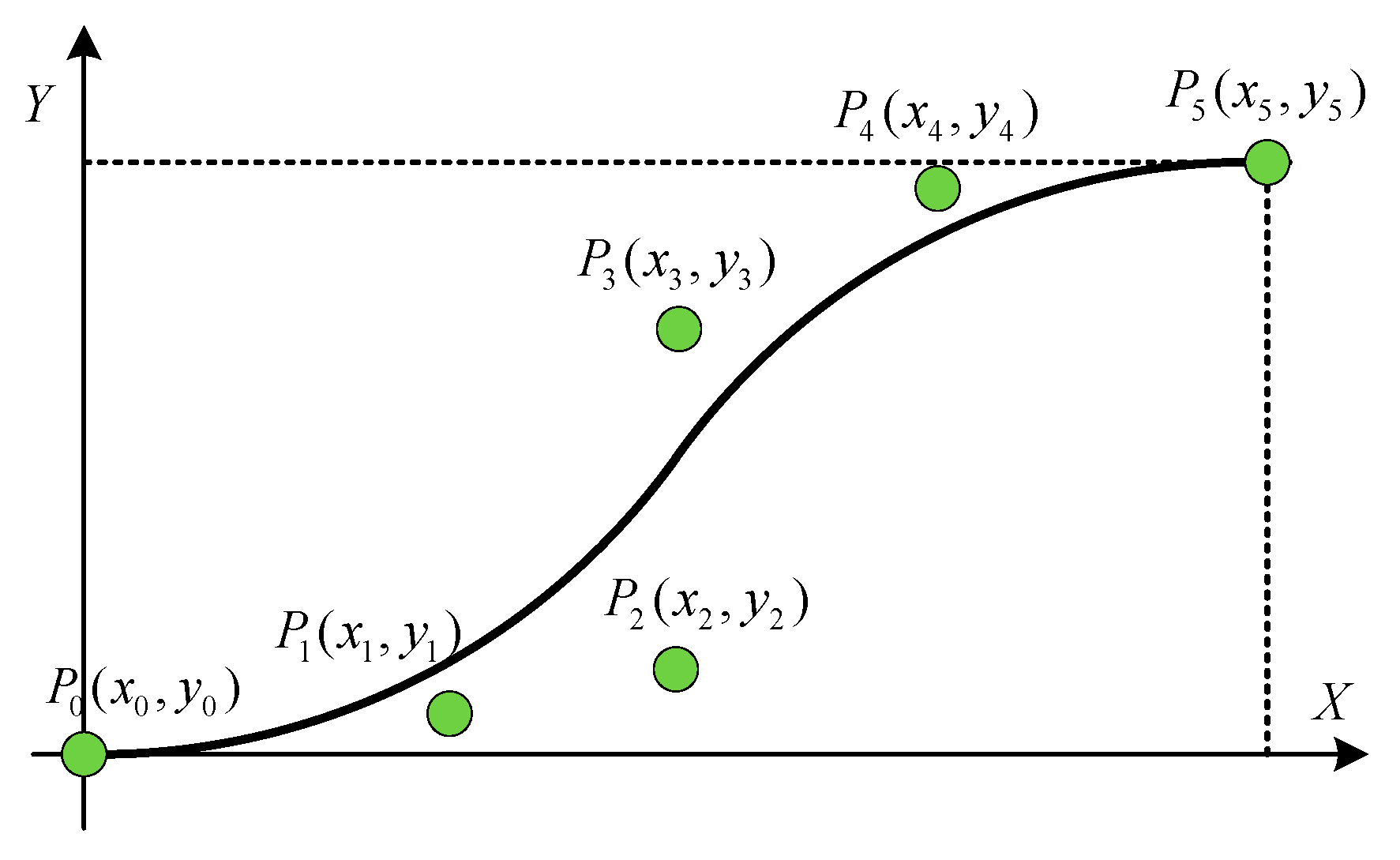
3.2. The Mode Switching Method Based on Optimal Bézier Curve of MOPSO

After finishing the design of the system controller, its response characteristics are determined. Current surges caused by sudden changes of the reference signal will threaten the circuit safety. During the mode switching period, the current response curve will be smoother if the appropriate switching reference signal is used.
When the reference current of the system is i ref ( t ) , the response i(t) of the system can be obtained according to the system transfer function. Then, the optimal mode switching problem can be equivalent to the multi-objective optimization problem by finding the optimal switching function i ref ( t ) under the condition that the system transfer function is G(s). The optimization goal is to minimize the value of overshoot and find the shortest response time. The optimization model is shown in Equation (7):
min f 1 = min { σ i [ i refi ( t ) ] } f 2 = min { t si [ i refi ( t ) ] } s . t t 1 t t 2
where, σ i is the overshot of the current, t si is the response time, t 1 is the start time of the mode switching, t 2 is the end time of the mode switching.
First published in 1962 by the French engineer Pierre Bézier, the Bézier curve with good smoothing characteristics is widely used for trajectory planning and auto body design [21,22,23]. The n-order Bézier curve can be determined by the given point P 0 , P 1 P n which is expressed by the parametric expression shown in Equation (8):
B ( μ ) = i = 0 n ( n i ) P i ( 1 μ ) n i μ i = ( n 0 ) P 0 ( 1 μ ) n μ 0 + ( n 1 ) P 1 ( 1 μ ) n 1 μ 1 + + ( n n 1 ) P n 1 ( 1 μ ) 1 μ n 1 + ( n n ) P n ( 1 μ ) 0 μ n
where, μ is the equation parameter, which is in the range of [0, 1].
In this paper, the 5th-order Bézier curve is used for mode switching trajectory planning. In the two-dimensional plane coordinate system, the x coordinate represents time and the y coordinate represents the reference current which are functions of the parameter μ. The mode switching trajectory based on the 5th-order Bézier curve is shown in Equation (9):
{ x = x 0 ( 1 μ ) 5 + 5 x 1 μ ( 1 μ ) 4 + 10 x 2 μ 2 ( 1 μ ) 3 + 10 x 3 μ 3 ( 1 μ ) 2 + 5 x 4 μ 4 ( 1 μ ) + x 5 μ 5 y = y 0 ( 1 μ ) 5 + 5 y 1 μ ( 1 μ ) 4 + 10 y 2 μ 2 ( 1 μ ) 3 + 10 y 3 μ 3 ( 1 μ ) 2 + 5 y 4 μ 4 ( 1 μ ) + y 5 μ 5
where y is the reference current, x is the time.
The optimal mode switching problem is to find a Bézier curve determined by points P 0 , P 1 P 5 , which can be obtained by solving Equation (7).
Particle Swarm Optimization (PSO) [21] was proposed by Kennnedy and Eberhart in 1995. The algorithm is inspired by birds’ preying behavoir, and then uses swarm intelligence to search continuously in solution space to obtain the optimal solution. PSO is a group-based optimization tool, which is an effective optimization tool for nonlinear optimization problems, combinatorial optimization problems and nonlinear mixed-integer optimization problems. The velocity and position of particles can be calculated according to the following formula:
v ij k + 1 = w × v ij k + c 1 × r 1 × ( p b e s t ij k x ij k ) + c 2 × r 2 × ( g b e s t ij k x ij k )
x ij k + 1 = x ij k + v ij k + 1
where, v ij k is the velocity of particle i at iteration k; k is the pointer of iterations; w is the inertia weight factor; c 1 , c 2 is the acceleration constant; r 1 , r 2 is the random number between 0 and 1; p b e s t ij is extreme value of particle i; g b e s t ij is the extreme value of the group; x ij k is the current position of particle i at iteration k.
According to Equation (5), if the Laplace transform of the Bézier curve is Rb,p6(s), the inductor current response of Bi-DC/DC is shown in Equation (12):
C ( s ) = R b , p 6 ( s ) G c ( s ) G id ( s ) 1 + G c ( s ) G id ( s )
where, Rb,p6(s) is determined by 5th order Bezier curve.
As shown in Equation (12), the time-domain response of the inductor current can be obtained by inverse Laplace transform. The multi-objective optimization model is shown in Equation (13):
min f 1 = min { σ i [ 1 ( R b , p 6 ( s ) G c ( s ) G id ( s ) 1 + G c ( s ) G id ( s ) ) ] } f 2 = min { t si [ 1 ( R b , p 6 ( s ) G c ( s ) G id ( s ) 1 + G c ( s ) G id ( s ) ) ] } s . t t 1 t t 2
where, σ i is the current overshot which can be obtained by the response of the inductor current. t si is the time taken for the steady-state value of inductor current rise from 5% to 95%.
The control coordinates of the Bézier curve are the parameters need to be optimized in Equation (13). After using the multi-objective particle swarm optimization (MOPSO)optimization method proposed in literature [22], the control coordinates of the Bézier curve can be optimized.

3.3. Analysis of Mode Switching Process

Because the MOPSO proposed by Coello [22,23] is one of the most classical MOPSO algorithm, so it is adopted to solve the multi-objective problem in this paper. Assume that the switching signal can transit to the steady state input value within 10 ms. The goal of optimization is to obtain the 5th-order Bézier curve determined by six points shown in Figure 7, then the index corresponding to the output response is optimized by switching along the curve.
In order to optimize the solution of the Equation (9), the transfer function is constructed based on the above parameters, and the system response under different switching signals is obtained. The Pareto front is the optimal solution set for multi-objective problems, which is shown in Figure 8. Since any solution from Pareto front satisfies the optimal theory, one of the solutions is selected as the switching signal to obtain the response of system.
The current response of different switching signals is shown in Figure 9 as compared with direct switching and switching along line. As shown in Figure 9, i r e f 1 is the direct switching current which is obtained by directly switching from the initial value to the end value without a transition at given switching point, i 1 is the current response of direct switching; i r e f 2 is the current which is obtained by switching from initial value to the end value along a straight line, and i 2 is the relevant current response; i r e f 3 is the optimal Bézier curve, i 3 represents its current response.
The system based on the optimal Bézier curve can realize mode switching without overshoot and the stabilization time is significantly shorter than those of the other two methods.

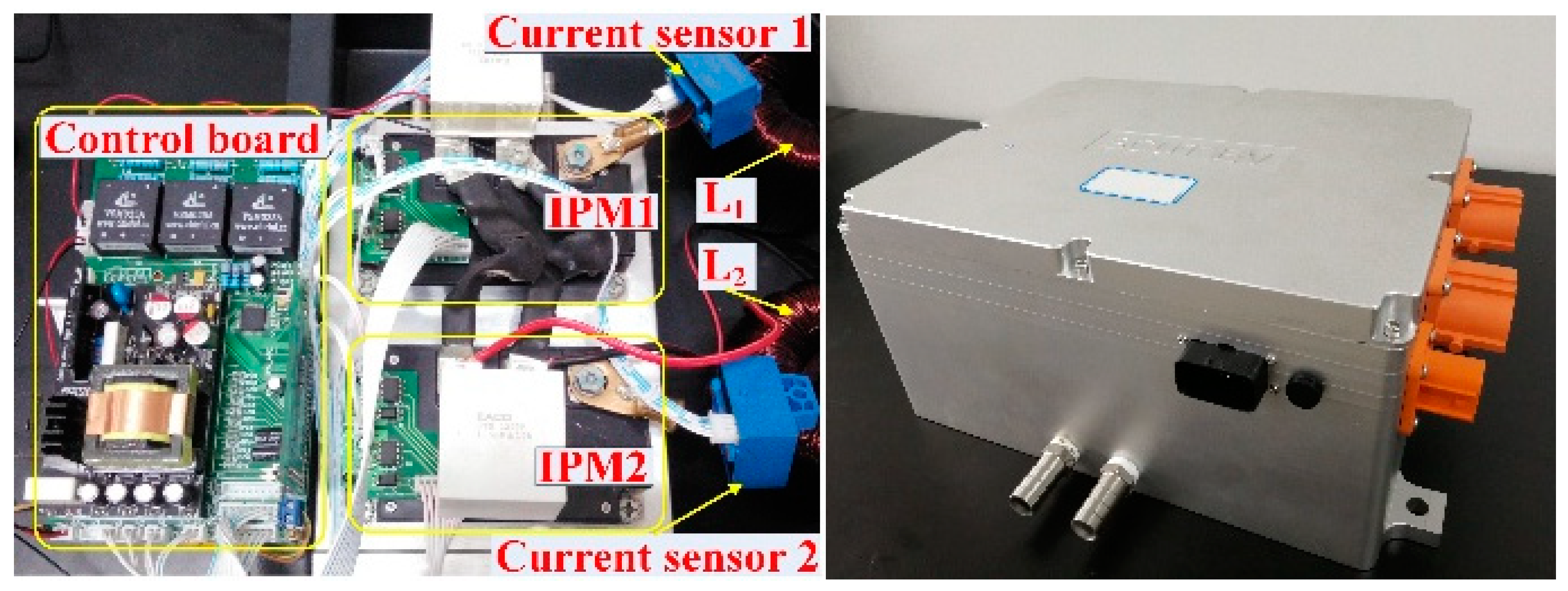
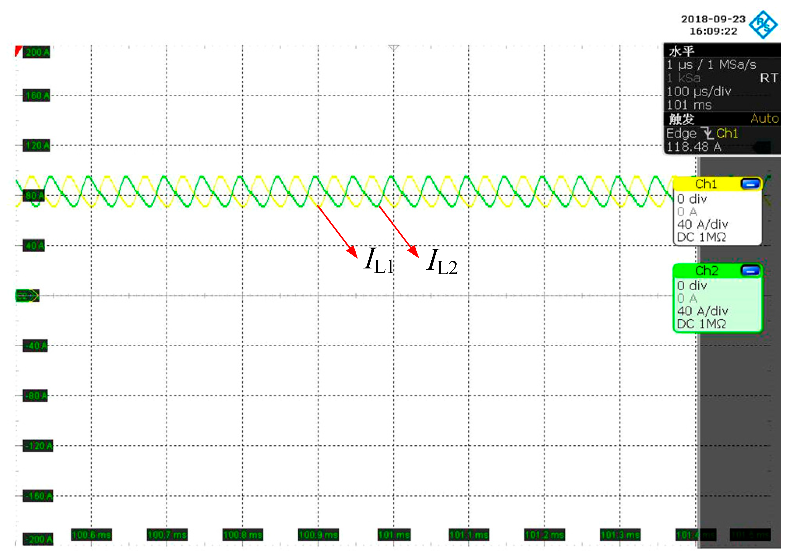
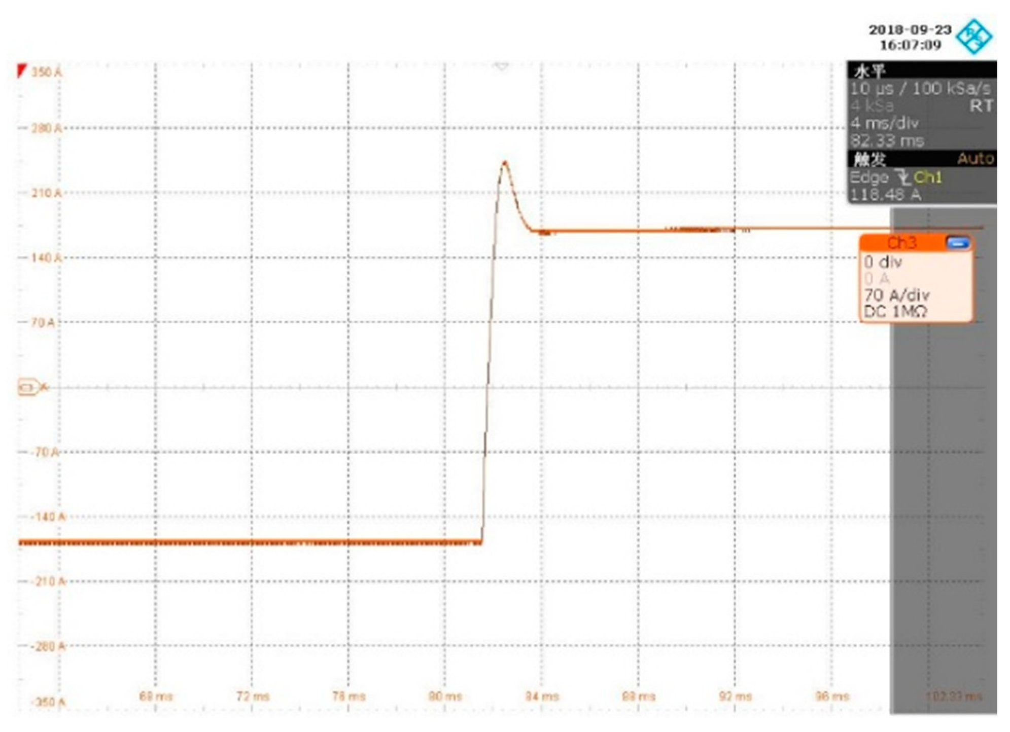
4. Experimental Results

According to the design requirements of a certain vehicle model, Bi-DC/DC needs to achieve bidirectional DC conversion between the super capacitor pack and the lithium-ion battery pack, i.e., the conversion from single-phase AC to lithium-ion battery pack, and the conversion from lithium-ion battery pack to single-phase AC. The performance requirements of the Bi-DC/DC are shown in Table 1.
For the Bi-DC/DC mode, the inductance of L1, L2 are selected as 69 uH, while the rated current is 150 A. High-voltage DC end filter capacitor C2 contains two 4700 μF/500 V aluminum electrolytic capacitors; and low-voltage DC end C1 contains a 2200 μF/400 V aluminum electrolytic capacitor. The four switches are consisting of two Mitsubishi PM200DV1A120 IPM modules. The current is sampled by LEM’s HAS-200-s Hall current sensor, while the voltage is sampled in an isolated way by CHIEFUL’s VSM025A Hall voltage sensor. The voltage and current waveform are collected by R&S RTE1024 oscilloscope. The main components of the prototype are shown in Figure 10.
In Bi-DC/DC mode, the maximum power tested is 4 kW due to the limitation of the test equipment. The output current of the low voltage DC terminal is 175 A, and the two-phase switches turn on alternately by 180°. The inductor current in Boost mode is shown in Figure 11. IL1 and IL2 represent the inductor current of L1 and L2, respectively, while IL is the sum of the two currents.
When Bi-DC/DC mode switching is carried out, the current of the low voltage DC terminal is switched from −175 A to 175 A in the switching from Buck mode to Boost mode. Firstly, step switching is carried out for mode switching, and the output current in the switching process is shown in Figure 12. The switching current impulse is 252 A, resulting in 44% overshoot. When the steady-state value changes from 5% to 95%, the switching time is 1.33 ms.
The current is out of control for a period at the beginning of the switching process, as shown in Figure 13.
Then, the switching is conducted based on a constant slope straight line, the resulting output current in the switching process is shown in Figure 14 with a switching time of 3.15 ms.
Finally, the optimal Bézier curve is used for mode switching, the output current during the switching process is shown in Figure 15. The switching time is 2.52 ms and there is no overshoot in the switching process.
Based on the above results, the switching times of the three methods are all less than 4 ms, all of them can track the reference power of the controller more efficiently. But if the step switching is carried out, the current inrush will be greater. By contrast, the Bézier curve can be used to achieve the mode switching in a shorter time (2.52 ms) and without any overshoot.

5. Conclusions

In the process of Boost and Buck mode switching, the Bi-DC/DC will produce a large current inrush which threatens the safety of the circuit. In order to solve this problem, a method of mode switching based on optimal Bézier curve for Bi-DC/DC is proposed, and a prototype is made for experimental verification. The following conclusions are drawn:
(1)
When Bi-DC/DC mode switching with step signal is carried out, the process will be out of control and a large current overshoot will be generated at its beginning. The result of the prototype test shows that the step switching method produces 44% overshoot.
(2)
The current overshoot can be avoided when the mode switching is carried out by a constant slope linear switching method, but the switching time will be prolonged.
(3)
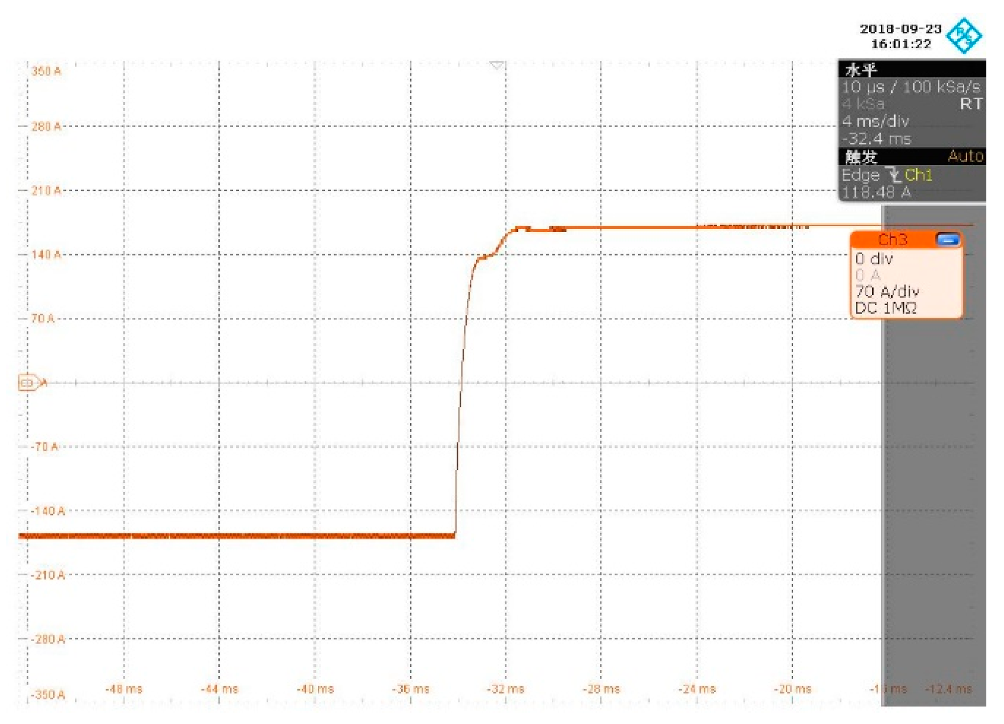
A fast and non-overshoot mode switching can be achieved when switching is performed based on the optimized Bézier curve. Using this optimal mode switching method, the prototype test results show that there is no overshoot when the load current is switched from −175 A to 175 A, and the switching time is 2.52 ms.

Author Contributions

Conceptualization was made by F.W. and Y.L.; Supervision and Project Administration were made by Y.L.; Validation were made by F.W. and H.L.; Software were made by X.X.; All authors contributed to Formal Analysis, Investigation and Writing.

Funding

This research was funded by the Major Research and Development Project of Guangdong Science and Technology Department, grant number 2016B010132001.

Conflicts of Interest

The authors declare no conflict of interest.

References

  1. Zhai, L.; Zhang, T.; Cao, Y.; Yang, S.P.; Kavuma, S.; Feng, H.Y. Conducted EMI Prediction and Mitigation Strategy Based on Transfer Function for a High-Low Voltage DC-DC Converter in Electric Vehicle. Energies 2018, 11, 1028. [Google Scholar] [CrossRef]
  2. Han, D.; Noppakunkajorn, J.; Sarlioglu, B. Comprehensive Efficiency, Weight, and Volume Comparison of SiC- and Si-Based Bidirectional DC–DC Converters for Hybrid Electric Vehicles. IEEE Trans. Veh. Technol. 2014, 63, 3001–3010. [Google Scholar] [CrossRef]
  3. Pahlevaninezhad, M.; Drobnik, J.; Jain, P.K.; Bakhshai, A. A Load Adaptive Control Approach for a Zero-Voltage-Switching DC/DC Converter Used for Electric Vehicles. IEEE Trans. Ind. Electron. 2012, 59, 920–933. [Google Scholar] [CrossRef]
  4. Dusmez, S.; Hasanzadeh, A.; Khaligh, A. Comparative Analysis of Bidirectional Three-Level DC-DC Converter for Automotive Applications. IEEE Trans. Ind. Electron. 2015, 62, 3305–3315. [Google Scholar] [CrossRef]
  5. Cortez, D.F.; Waltrich, G.; Fraigneaud, J.; Miranda, H.; Barbi, I. DC-DC Converter for Dual-Voltage Automotive Systems Based on Bidirectional Hybrid Switched-Capacitor Architectures. IEEE Trans. Ind. Electron. 2015, 62, 3296–3304. [Google Scholar] [CrossRef]
  6. Luo, Y.; Wang, F. Creation of parameter model for the efficiency of Bi-DC/DC in electric vehicle and affecting factor analysis. Qiche Gongcheng/Autom. Eng. 2016, 38, 1396–1401. [Google Scholar]
  7. Wen, H.; Su, B. Hybrid-mode interleaved boost converter design for fuel cell electric vehicles. Energy Convers. Manag. 2016, 122, 477–487. [Google Scholar] [CrossRef]
  8. Chen, S.J.; Yang, S.P.; Huang, C.M.; Chou, H.M.; Shen, M.J. Interleaved High Step-Up DC-DC Converter Based on Voltage Multiplier Cell and Voltage-Stacking Techniques for Renewable Energy Applications. Energies 2018, 11, 1632. [Google Scholar] [CrossRef]
  9. Garcia, O.; Zumel, P.; De Castro, A.; Cobos, J.A. Automotive DC-DC bidirectional converter made with many interleaved buck stages. IEEE Trans. Ind. Electron. 2006, 21, 578–586. [Google Scholar] [CrossRef]
  10. Zdanowski, M.; Rabkowski, J.; Barlik, R. Highly-Efficient and Compact 6 kW/4 x 125 kHz Interleaved DC-DC Boost Converter with SiC Devices and Low-Capacitive Inductors. Energies 2017, 10, 363. [Google Scholar] [CrossRef]
  11. Urciuoli, D.P.; Tipton, C.W. Development of a 90 kW bi-directional DC-DC converter for power dense applications. In Proceedings of the Twenty-First Annual IEEE Applied Power Electronics Conference and Exposition, Dallas, TX, USA, 19–23 March 2006; p. 4. [Google Scholar]
  12. Calderon-Lopez, G.; Forsyth, A.J.; Nuttall, D.R. Design and Performance Evaluation of a 10-kW Interleaved Boost Converter for a Fuel Cell Electric Vehicle. In Proceedings of the CES/IEEE International Power Electronics and Motion Control Conference (IPEMC 2006), Shanghai, China, 14–16 August 2006; pp. 1–5. [Google Scholar]
  13. Thounthong, P.; Sethakul, P.; Rael, S.; Davat, B. Design and implementation of 2-phase interleaved boost converter for fuel cell power source. In Proceedings of the 4th IET International Conference on Power Electronics, Machines and Drives (PEMD 2008), York, UK, 2–4 April 2008; pp. 91–95. [Google Scholar]
  14. Xu, H.; Wen, X.; Qiao, E.; Guo, X. High Power Interleaved Boost Converter in Fuel Cell Hybrid Electric Vehicle. In Proceedings of the IEEE International Conference on Electric Machines and Drives, San Antonio, TX, USA, 15 May 2005; pp. 1814–1819. [Google Scholar]
  15. Huang, X.; Nergaard, T.; Lai, J.S.; Xu, X. A DSP based controller for high-power interleaved boost converters. In Proceedings of the Eighteenth Annual IEEE Applied Power Electronics Conference and Exposition, Miami Beach, FL, USA, 9–13 February 2003; Volume 1, pp. 327–333. [Google Scholar]
  16. Xinquan, L.; Jianping, G.; Weixue, Y.; Yu, C. A novel digital soft-start circuit for DC-DC switching regulator. In Proceedings of the International Conference on ASIC, Shanghai, China, 24–27 October 2006. [Google Scholar]
  17. Zhou, M.; Sun, Z.; Low, Q.W.; Siek, L. Fast transient response DC-DC converter with start-up in-rush current control. Electron. Lett. 2016, 52, 1883–1885. [Google Scholar] [CrossRef]
  18. Zhao, C.; Round, S.; Kolar, J.W. Buck and boost start-up operation of a three-port power supply for hybrid vehicle applications. In Proceedings of the 36th IEEE Power Electronics Specialists Conference, Recife, Brazil, 16 June 2005; pp. 1851–1857. [Google Scholar]
  19. Kondo, R.; Higaki, Y.; Yamada, M. Proposition and experimental verification of a bi-directional isolated DC/DC converter for battery charger-discharger of electric vehicle. In Proceedings of the Applied Power Electronics Conference and Exposition, Long Beach, CA, USA, 20–24 March 2016. [Google Scholar]
  20. Basso, C.P. Switch-Mode Power Supplies—SPICE Simulations and Practical Designs; McGraw-Hill, Inc.: New York, NY, USA, 2014. [Google Scholar]
  21. Kennedy, J.; Eberhart, R. Particle swarm optimization. In Proceedings of the ICNN95—International Conference on Neural Networks, Perth, Australia, 27 November–1 December 1995. [Google Scholar]
  22. Coello, C.A.C.; Lechuga, M.S. MOPSO: A proposal for multiple objective particle swarm optimization. In Proceedings of the 2002 Congress on Evolutionary Computation, Honolulu, HI, USA, 12–17 May 2002; pp. 1051–1056. [Google Scholar]
  23. Garcia, I.C.; Coello, C.A.C.; Arias-Montano, A. MOPSOhv: A New Hypervolume-based Multi-Objective Particle Swarm Optimizer. In Proceedings of the 2014 IEEE Congress on Evolutionary Computation (CEC), Beijing, China, 6–11 July 2014; pp. 266–273. [Google Scholar]
Figure 1. Topology structure of the Bi-DC/DC.
Energies 12 00378 g001
Figure 2. The operating states of Bi-DC/DC mode (the switch is: (a) turned on, (b) turned off) under Buck mode.
Energies 12 00378 g002
Figure 3. Block diagram of Bi-DC/DC control mode.
Energies 12 00378 g003
Figure 4. (a) Bode diagram of duty cycle to inductance current.; (b) Control block diagram of the system.
Energies 12 00378 g004aEnergies 12 00378 g004b
Figure 5. The equivalent circuit of switching process: (a) normal operation; (b) mode switching.
Energies 12 00378 g005
Figure 6. Waveform during mode switching.
Energies 12 00378 g006
Figure 7. The schematic illumination of 5th-order Bézier curve.
Energies 12 00378 g007
Figure 8. The optimal result of Pareto front.
Energies 12 00378 g008
Figure 9. Current response.
Energies 12 00378 g009
Figure 10. Photograph of the Bi-DC/DC prototype.
Energies 12 00378 g010
Figure 11. Inductor current waveform (100 μs/div, 40 A/div).
Energies 12 00378 g011
Figure 12. The current curve obtained by step switching: low side output current (4 ms/div, 70 A/div).
Energies 12 00378 g012
Figure 13. The inductor current during the switching process.
Energies 12 00378 g013
Figure 14. The current curve obtained by constant slope linear switching: low side output current (4 ms/div, 70 A/div).
Energies 12 00378 g014
Figure 15. The current curve obtained by optimal Bézier curve switching: low side output current (4 ms/div, 70 A/div).
Energies 12 00378 g015
Table 1. Design parameters of the Bi-DC/DC.
ParameterValue
High side voltage range280–420 V
Low side voltage range110–230 V
Rated inductor current250 A

