1. Introduction
Since it is common for equipment to work for 24 hours a day in industry applications, the equipment must therefore record the current conditions when it is shut down, and initiate the necessary processing procedures. Hence, a dual power source switch circuit is necessary to turn on the backup battery power source to ensure that the system can continue to work at the moment of the main power failure. Generally, the simplest method is to connect the main power supply and the backup power supply to the anodes of two diodes respectively, and the cathodes of the two diodes are coupled together to the load [
1,
2]. This method is simple and the problem of mutual feedback between the two power supplies can be avoided. However, in addition to the output voltage loss due to the diode voltage drop, when the power voltages of the dual power supplies are relatively close, both power sources will supply power to the load simultaneously. Therefore, it is not suitable for dual power switching applications. In
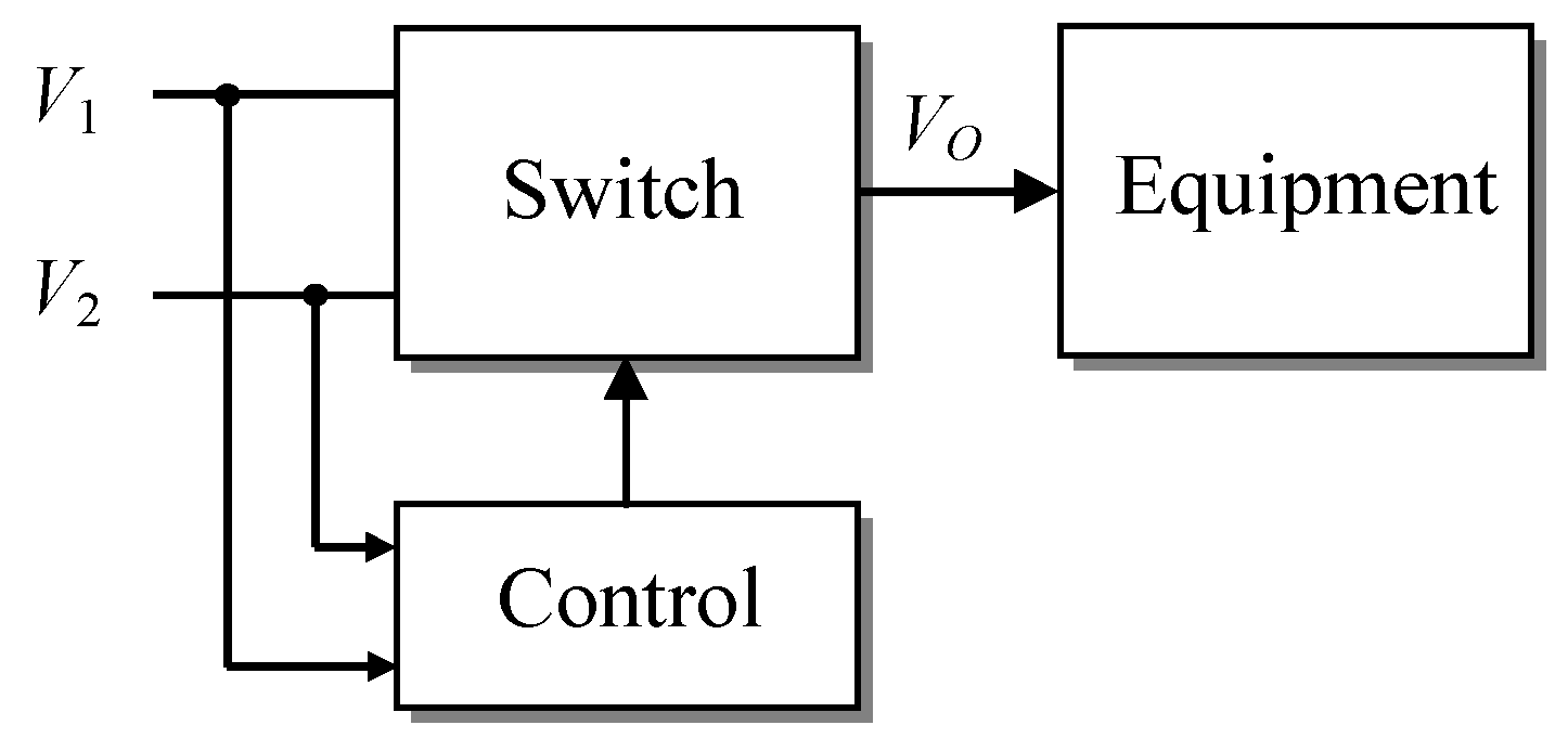
Figure 1, we show the basic schema of the dual power source switch. At the moment of the main power failure, the equipment should not be restarted due to the power source being switched to backup power. The switch shown in
Figure 1 cannot be the mechanical type like relay, which has a longer switching time. Since MOSFET switches have a faster switching speed, and their on-resistance is extremely low, the power PMOS is often used as a switching transistor [
3].
One reference [
4] pointed out that Pavio et al. proposed dual DC source switching technology, which was an effective method for switching between the power that was supplied from the fuel cell and the secondary power source. Chen et al. [
5] proposed dual AC source switching technology which was one of the key technologies to ensure power supply for important loads. During the switching process, the two power supplies usually have asynchronous characteristics, so that the zero-second switching affects the load and interferes with its normal operation and even burns down. From the previous description, it is understood that the circuit design for automatic switching between the main power supply and the backup power supply must meet the following functional requirements:
When the main power is present, the equipment is supported by the main power supply; when the main power supply is shut down, the automatic switch is applied to allow the backup power supply to support the equipment.
The two sets of power sources must be completely independent and cannot mutually give feedback to each other.
Voltage loss due to switching should be reduced as much as possible, regardless of whether the power supply is switched to the main or backup power source.
The major contributions of this paper include: (a) the design of an innovative dual power source switch circuit with a low loss output; (b) a mutual blocking control technology proposed to solve the voltage feedback problem existing in the conventional dual power switching design and (c) the demonstration of the proposed dual power source switch circuit implemented and analyzed.
This paper is organized as follows:
Section 2 reviews the control methods of dual power switching techniques;
Section 3 introduces the proposed dual power switching using mutual blocking technology;
Section 4 illustrates the experimental results and analysis; and
Section 5 concludes the experimental results of this paper.
2. Control Methods of Dual Power Switching
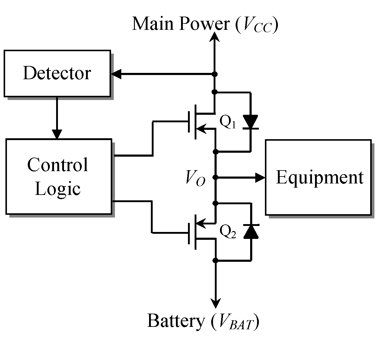
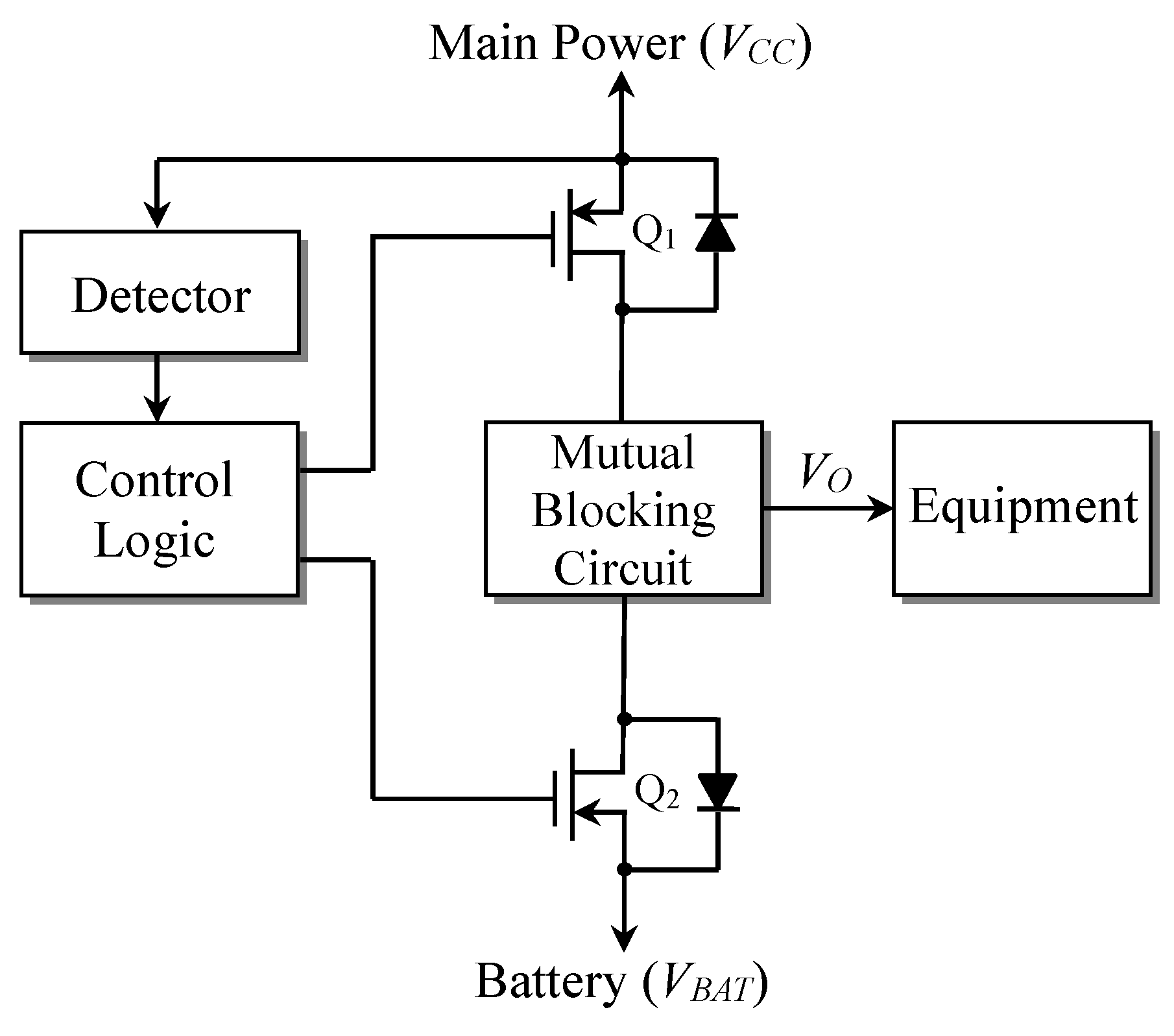
As seen in
Figure 2, the switches in a dual power switching design often use two power PMOS transistors, which their source nodes are connected together. The purpose of this is to achieve faster switching and reduce conductive voltage loss. The switching control can be either a conventional control method using the main power detection, or a control method using a dedicated chip. These two methods are described in detail below.
2.1. Control Method Using Main Power Detection
It is simplest to directly control the switching of dual power sources based on detecting the presence or absence of main power. In this traditional design architecture shown in
Figure 2, only a common voltage detector IC such as TC54 [
6] or MAX6376 [
7] is needed to detect if the main power supply from the utility is shut down. In addition, two low power NMOS transistors can be used as the control logic switches [
8] as seen in
Figure 3. According to the state of the main power detected, the gate voltages of Q
1 and Q
2 can be controlled, where Q
1 and Q
2 are connected to main power supply (
VCC) and battery (
VBAT), respectively. Essentially, the output
VO to the equipment is given by:
where,
rDS1 and
rDS2 are conductive resistances of two PMOS (Q
1 and Q
2), respectively.
When the main power source is present, the output of the voltage detector can directly turn Q1 on by the reverse of an NMOS (QN1); and the reverse output of this NMOS can turn Q2 off through the reverse of another NMOS (QN2). Therefore, rDS1 approaches 0 and rDS2 is almost infinite such that VO equals VCC. Conversely, when only the battery power source is present, that causes Q1 to turn off and Q2 to turn on (i.e., rDS1 ≈ ∞ and rDS2 ≈ 0), and thus the power supplied to the equipment is switched to battery power (i.e., VO = VBAT).
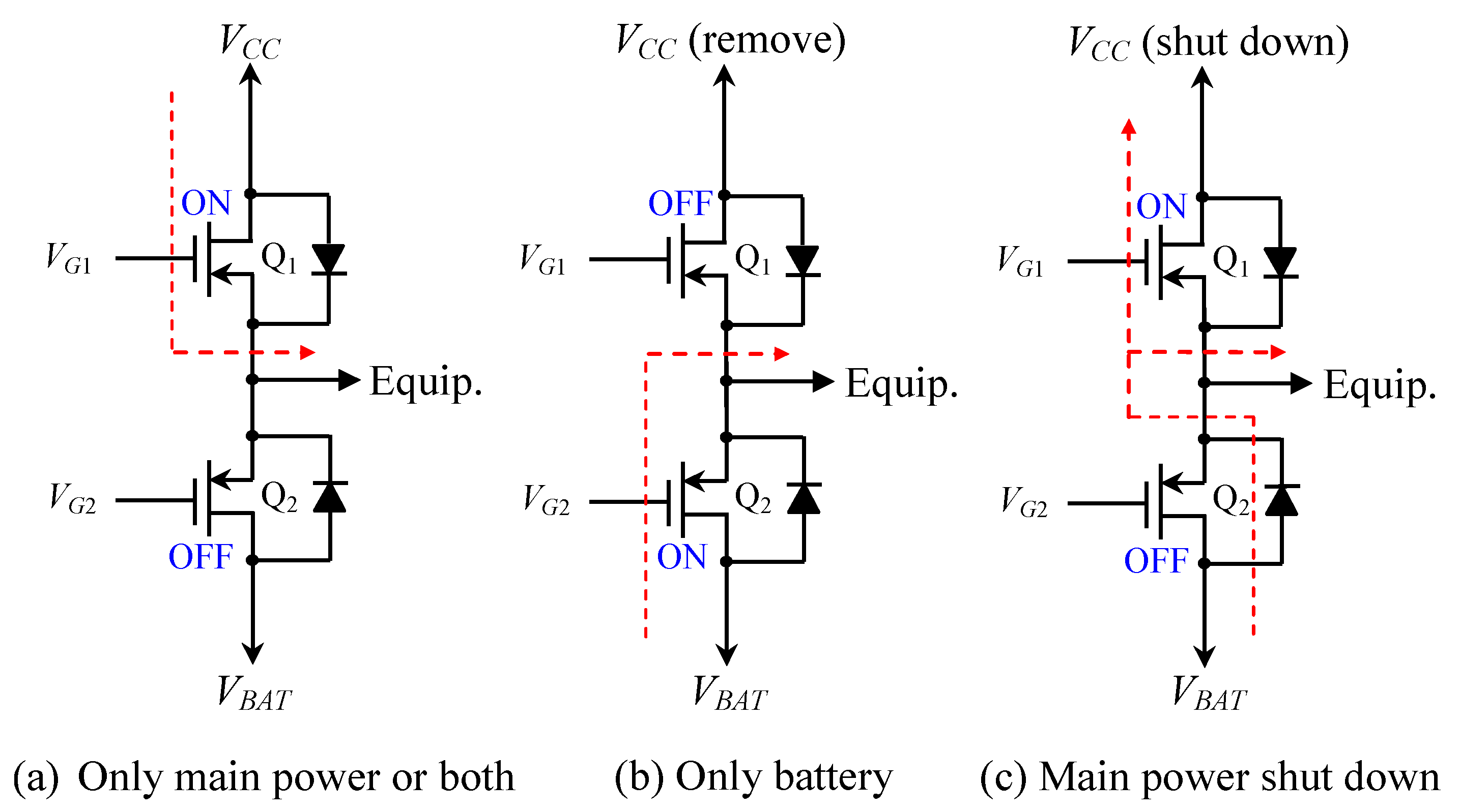
The operation principle of this circuit is as follows:
When the main power supply and the battery are both present, or only the main power supply is present, Q1 is on and Q2 is off, at this time the main power supply provides a low loss output to the equipment.
When only battery power supply is present, Q2 is on and Q1 is off, at this time, the battery power supply provides a low loss output to the equipment.
When the main power supply and battery power are both present but the main power supply is suddenly shut down, due to the characteristics of MOSFET delay transition [
9], the battery power supply is still fed back to the main power supply terminal via the delayed Q
1. Therefore, the voltage detector still regards the main power supply as active so that the controller still keeps Q
1 on and Q
2 off. At this time, the battery power supplying the equipment will suffer an internal diode voltage drop (
VD) of Q
2, and another power discharge path through Q
1 will be formed.
According to the description of operation state (3), the output voltage should be modified as:
where,
F denotes the presence factor of main power supply,
F = 1 indicates presence, otherwise
F = 0. Of course, if the sources of Q
1 and Q
2 are connected in a series with the diodes, respectively, and the cathodes of two diodes are connected to the equipment, then the power supply feedback problem can be avoided. However, in this condition, whether the main power or the battery power is present, the output voltage to the equipment will drop by passing through another diode.
Figure 4 shows the power supply paths of the three different operating conditions mentioned above.
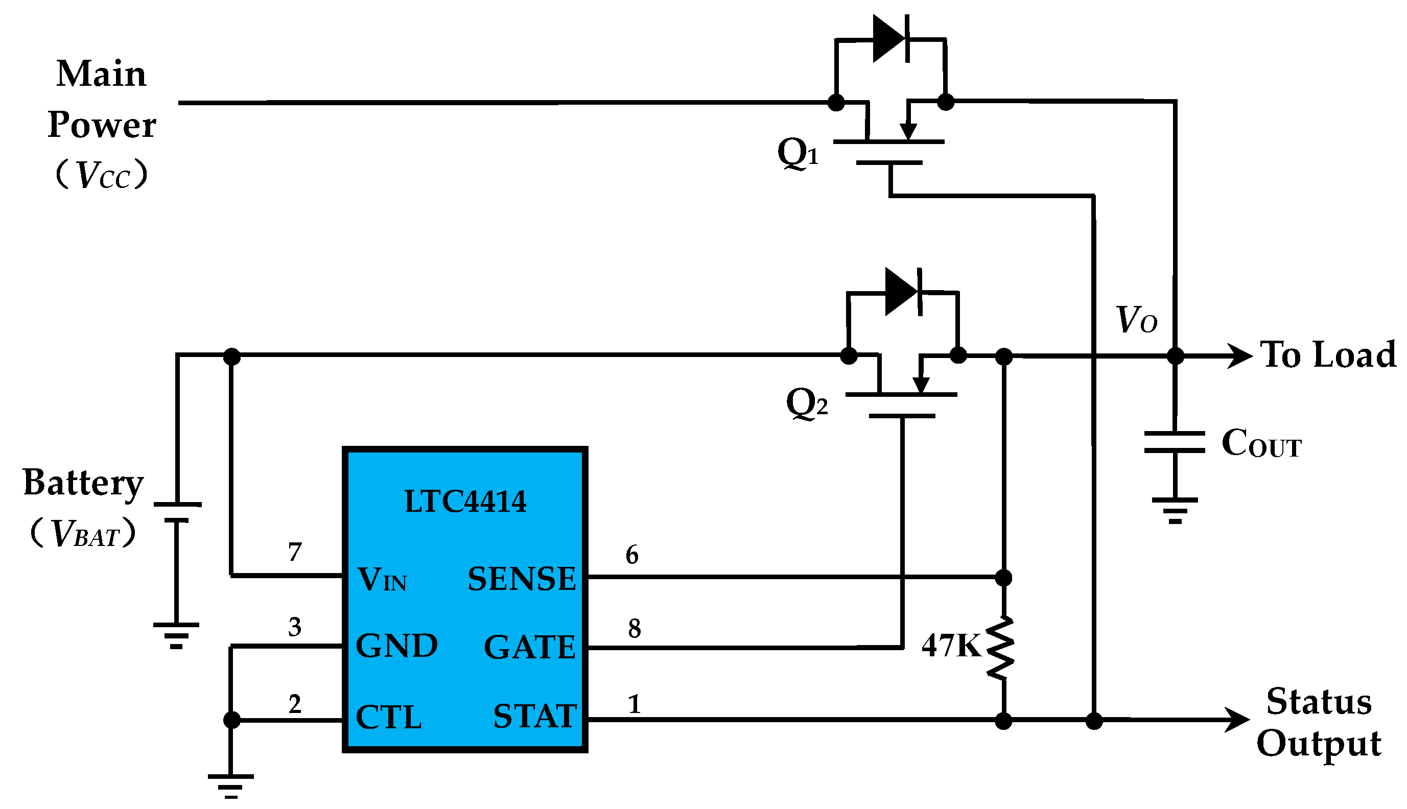
2.2. Control Method Using Dedicated Chip
In order to solve the above-mentioned problem of the battery voltage being fed back to the main power supply caused by the sudden power failure, using the operating amplifiers (OPA) with a fast response as the decision control when switching, is an often-used method [
8,
10]. In addition, they are integrated into the dedicated chips. Nowadays, one of dedicated control chips, such as LTC4414, has been developed by Linear Technology Semiconductor [
11], and it can be applied for dual power switching control shown in
Figure 5 [
11,
12], where
VCC is the main power supply and
VBAT is the battery power.
The circuit operation principle of
Figure 5 is as follows:
When only VCC is present and Q1 is on, but the GATE output voltage is not high enough that Q2 is not completely turned off and partial VCC is fed back to the battery terminal.
When VCC and VBAT are both present and VCC > VBAT, and thus Q1 is on and Q2 is off, the main power VCC has a low loss output to the equipment.
When only VBAT is present, and thus Q2 is on and Q1 is off, the battery power VBAT has a low loss output to the equipment.
When VCC and VBAT are both present, but VCC suddenly shuts down, Q1 turns off and Q2 turns on, and the battery power VBAT still maintains low loss output to the equipment.
When Vcc is restored, then power supply returns to state two. However, if VCC-VBAT < 0.5 V, Q2 is still on and Q1 is still off, the output VO cannot be switched back to VCC from VBAT.
According to the above operation principles, if the main power supply is suddenly shut down, the LTC4414 indeed can reduce output loss, when switching to battery power and not incur feedback to the main power terminal. If the main power supply is restored and the output is switched back to the main power again, the limiting condition is that the main power supply voltage must be more than 0.5 V higher than the battery voltage. In addition, if the battery voltage is much lower than the main power voltage, some of the voltage of the main power supply will feed back to the battery power terminal, and the equipment will not be able to obtain full supply voltage of the main power.
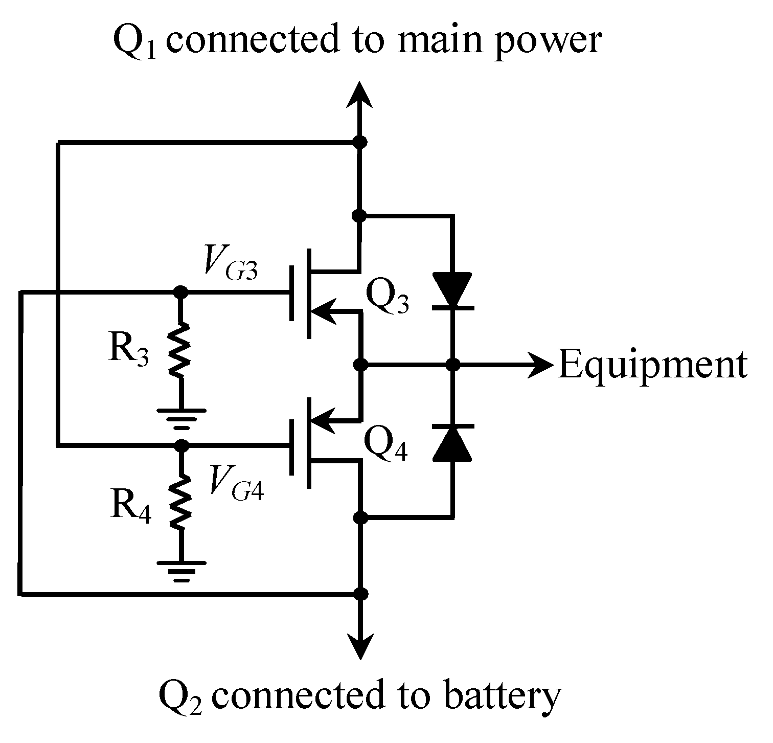
3. Dual Power Switching Using Mutual Blocking Technology
The conventional dual power switching design has the problem of voltage feedback, which is when the main power is shut down and the battery power not only provides the equipment with power, but also feeds voltage back to the main power supply terminal. Therefore, a battery discharge path forms, but this also shortens the battery supply hours. In this paper, we propose an innovative design architecture shown in
Figure 6. We still apply the voltage detector IC to determine the presence of a main power source, and separately control PMOS (Q
1) connected to the main power supply and PMOS (Q
2) connected to the battery by the NMOS control logic. However, unlike traditional designs, Q
1 and Q
2 are connected to the respective power inputs with their sources instead of their drains [
2]. In addition, two PMOS (Q
3 and Q
4) with the gate cross control and source docking are added to form a mutual blocking control circuit as shown in
Figure 7 to avoid voltage feedback. The circuit operation principle designed in this paper is as follows:
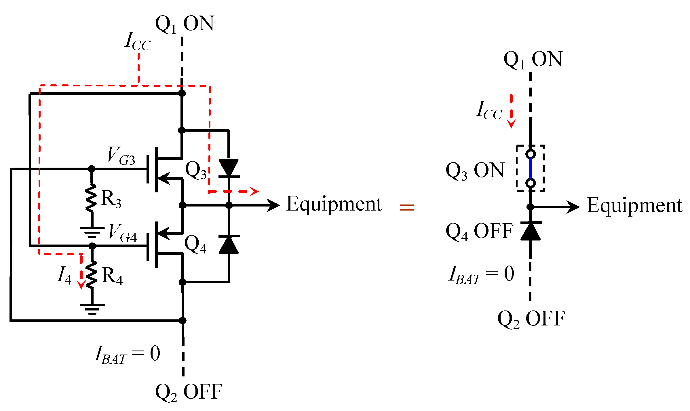
Considering that the main power supply and the battery power supply are both present, by detecting the presence of the main power supply, Q1 and Q3 will be on and Q2 and Q4 will be off.
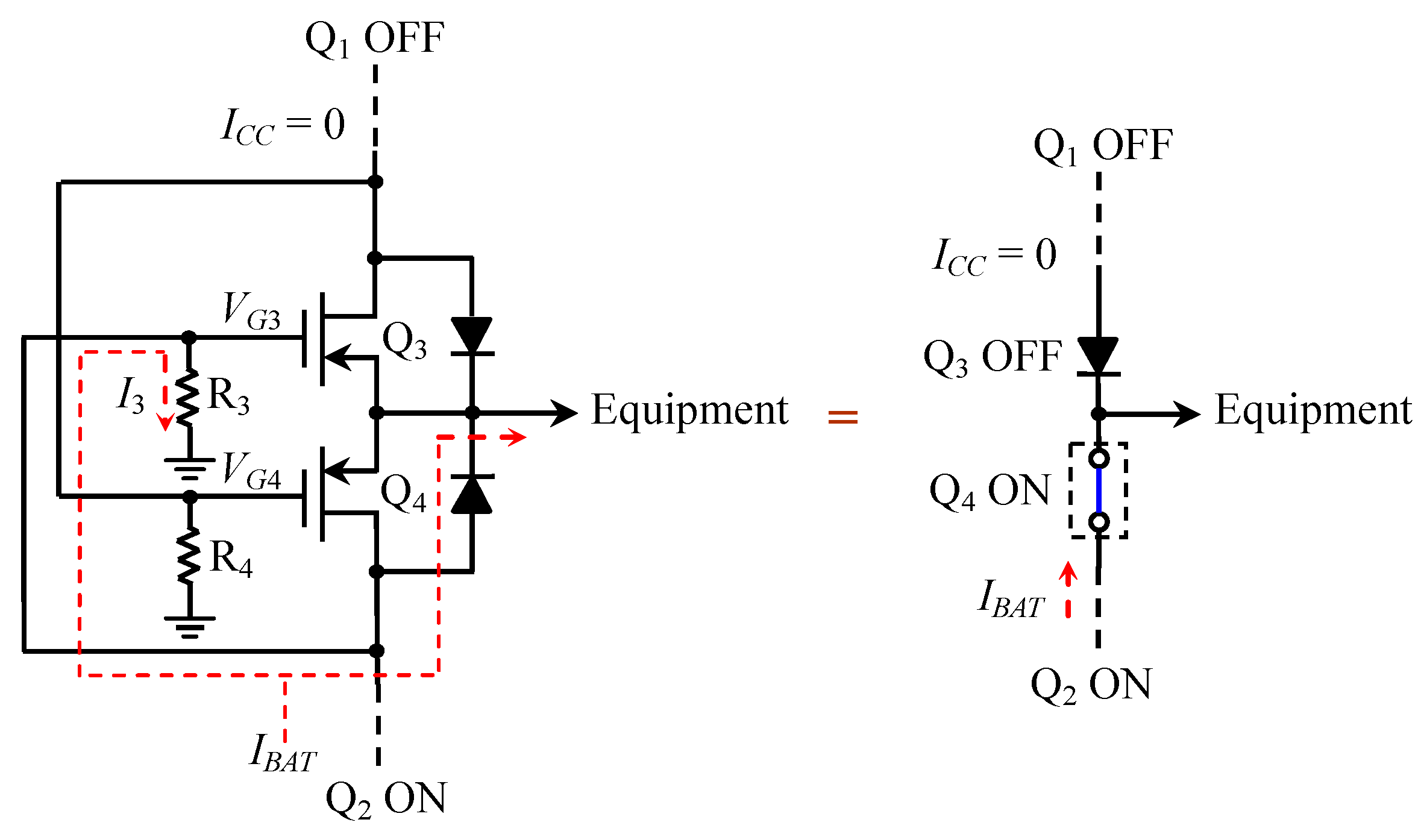
When the main power supply is shut down (i.e., its supply current ICC = 0), the control logic prepares to turn on Q2 and turn off Q1, although Q1 has not changed its operating state immediately, the voltage VG4 from the drain of Q1 is quickly lowered to zero, which will cause Q4 to turn on.
At this time, the voltage
VG3 from the drain of Q
2 rises to the battery voltage, which causes Q
3’s gate voltage to rise and turn off Q
3. By the diode inside Q
3, the battery voltage would not be fed back to the main power supply terminal, and thus the battery power supply can provide a low loss output for the equipment. This situation is shown in
Figure 8.
When the main power is restored, the control logic switches Q1 on and Q2 off, and VG3 is lowered due to the battery supply current IBAT = 0, thus causing Q3 to turn on.
At this time,
VG4 is raised to the main power supply voltage to turn off Q
4. As shown in
Figure 9, the internal diode of Q
4 prevents the main power from being fed back to the battery terminal, and the main power supply provides the equipment an output with low loss again.
In addition, if only the main power supply is present, or if the battery voltage is much lower than that of the main power supply, the design will not allow the main power supply voltage to give feedback to the battery terminal.
Therefore, from the equivalent circuit on the right side of
Figure 8 and
Figure 9, the roles of Q
3 and Q
4 are hereby equivalent to two approximately ideal dynamic diode switches. When they are turned on, there is only a very low voltage drop, and when they are turned off, their internal diodes can block the voltage feedback. Assume that the conductive resistances
rDS of Q
3 and Q
4 are zero in the ideal case, the output voltage to the equipment can be given by:
where,
S1(
t) is the control function of Q
3 to determine whether Q
3 is on or off, depending on
I3 from the battery supply current
IBAT. Similarly,
S2(
t) is used as the control function for Q
4 and is controlled by
I4 from the main power supply current
ICC. Equations (4) and (5) represent the control functions:
S1(
t) and
S2(
t), respectively, where
Vth is the threshold voltage of PMOS. Here,
R3 and
R4 should be ~MΩ to minimize these extra incurred current as possible.
Although this mutual blocking design adds two more PMOS, and the voltage loss of the power supply to the equipment slightly increases by one PMOS voltage drop, the voltage loss has been effectively reduced, compared with the general diode voltage drop. Particularly for equipment with a large load, the improvement in voltage and power loss is more obvious when the power PMOS with ultra low on-resistance is chosen. Meanwhile, it can effectively solve the problem of voltage feedback in the conventional design of dual power switching.
4. Experimental Results and Analysis
Basically, no matter which MOSFET-based dual power switching design is used, when power supply is switched, it will not cause the equipment to reset at the moment of switching. In order to verify the operation of different types of dual power switching design and compare the performances among them, under the same PMOS specifications, we have implemented three different types of dual power switching circuits including the conventional control type using the main power detection, the control type using dedicated chip, and the proposed mutual blocking control type.
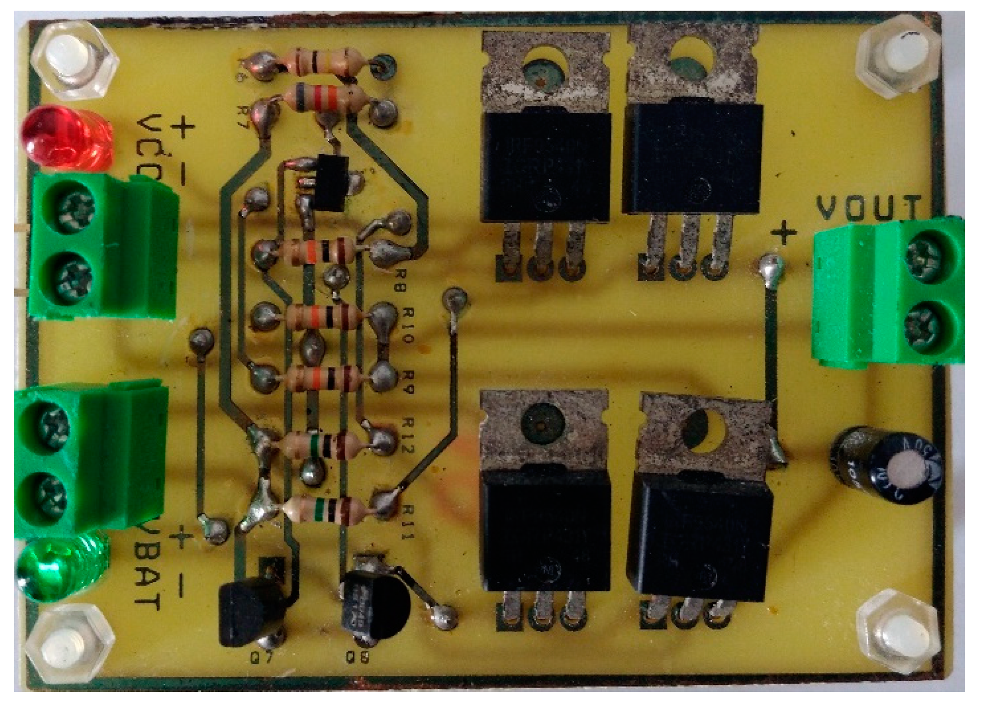
Figure 10 shows the circuit prototype of the proposed dual power source switch, where two other low power NMOS transistors are used as the control logic to turn on or turn off the two PMOS switches (Q
1 and Q
2), and the control logic circuit is the same as the circuit shown in
Figure 3. Here the main power voltage (
VCC = 12.2 V) comes from the utility power adapter, while the other power source is supplied by a lithium battery pack (
VBAT = 11.8 V). According to the various switching conditions, the performance of the three types of switching circuits are measured and compared. The maximum supply current to the equipment depends on the power PMOS used as a switch. In our experiments, all power PMOS transistors are the same component of IRF9540, and the maximum continuous drain current of IRF9540 [
13] is about 19 A.
4.1. Measured Waveforms
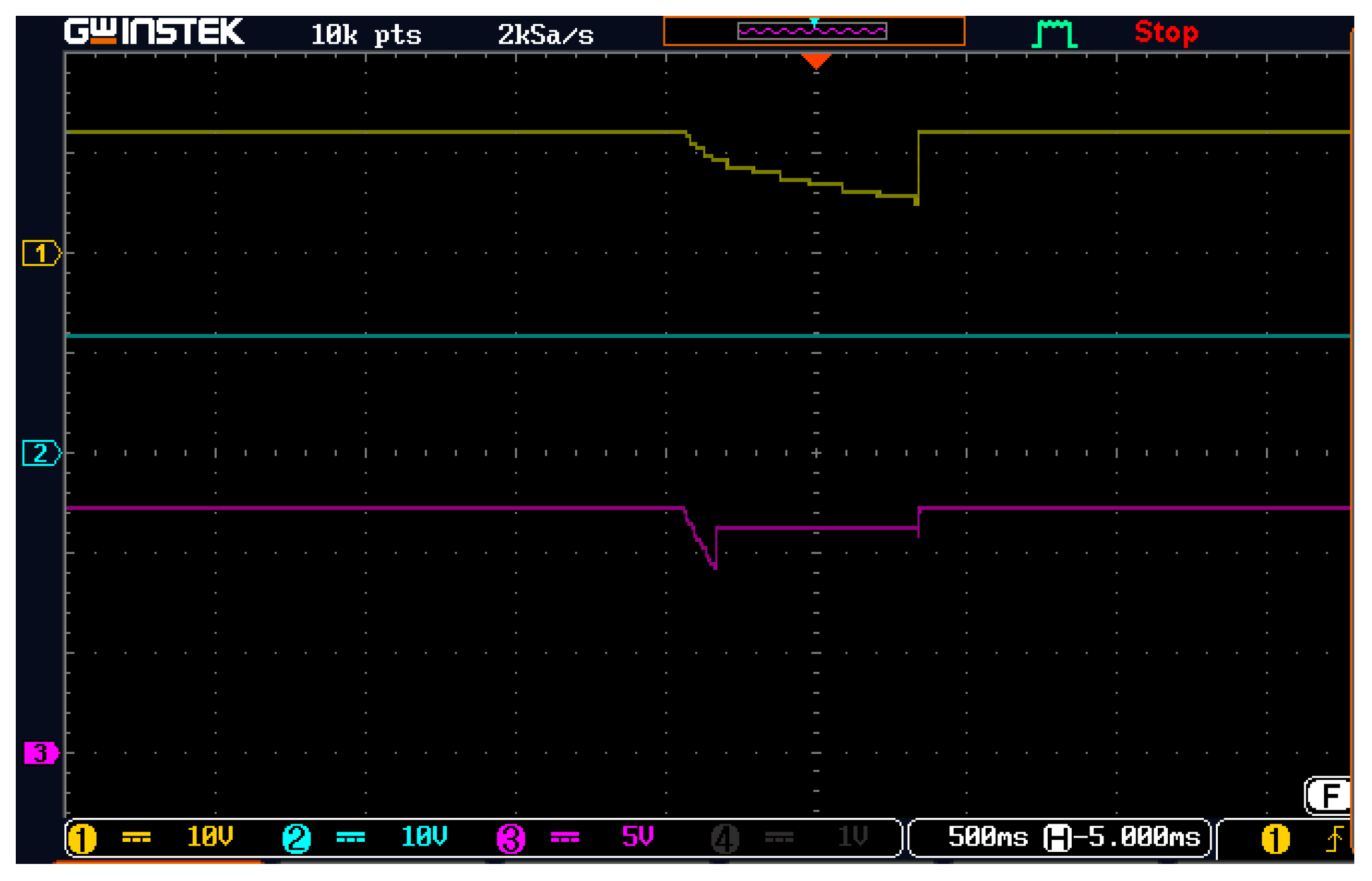
In the practical measurement, we try to observe the waveforms shown in
Figure 11 during switching, where CH1 represents the main power voltage, CH2 represents the battery voltage, and CH3 indicates the output voltage. For clearer observation, the battery voltage is adjusted to 11 V temporarily. When the main power voltage starts to drop, the output to the equipment is not switched to the battery supply immediately; that is because the main power voltage does not drop to the desired threshold voltage of the voltage detector IC. This threshold voltage depends on the voltage that ensures the equipment works correctly, where the threshold voltage is set to 9.27 V in the proposed design. When the main power is restored, the output to the equipment can be quickly switched back to the main power supply. The switching time of the proposed design is very short, only about a few μs, and it depends on the used PMOS.
4.2. Output Voltage and Power Loss
Using PMOS as a switching power transistor, the output voltage loss is extremely low in a fully conductive state. It can be seen from
Table 1 that only the switching circuit using the main power detection causes the battery output voltage to lose about 0.6 V when the main power supply is momentarily shut down. Whether the other switching circuits switch to the main power or the battery, the output to the equipment is almost equal to the original supply voltage. However, since the main power supply voltage is not greater than the battery voltage by more than 0.5 V in our experiment, if the dedicated chip control is applied to the switching circuit, the output cannot be switched back to the main power supply from the battery when the main power supply is restored. Whatever the main power supply is greater than the battery or not, the switching circuit using a mutual blocking control does not appear in the above situation.
Considering the different current levels of the load,
Table 2 shows the power loss during the turn-on caused by the power PMOS or the diode for different switching control methods. For the switching circuit using the main power detection control, the load current from the backup power supply will pass through an internal diode of PMOS when the main power supply is shut down. Thus, there exists a power loss caused by this internal diode. Although the power loss of the mutual blocking control is twice as large as that of the dedicated chip control due to the adding of one power PMOS on the load current path, the power loss caused by the power PMOS is still reduced compared with the power loss of the diode. If the power PMOS with ultra low on-resistance is further chosen, like PMN50XP [
14], the improvement in power loss will be more obvious even for large loads.
4.3. Output Voltage Feedback
A good design for dual power switching should consider that the two power supplies must be completely independent and does not mutually give feedback to each other. After the practical measurement shown in
Table 3, we find that the switching circuit using the main power detection control will feed battery voltage back to the main power supply terminal when the main power supply is momentarily shut down. When only the main power supply is present, or if the battery voltage is lower than that of the main power supply, the voltage feedback from the main power to the battery terminal also occurs in the switching circuit using a dedicated chip. However, if the mutual blocking control is adopted in the switching circuit, the two power supplies can be independent from each other under any condition, and they do not mutually give feedback to each other.
5. Conclusions
In addition to reducing circuit complexity, the use of commercial chips (such as the LTC4414) also effectively solves the voltage feedback problem of the conventional dual power switching design; and its output voltage retains the advantage of low loss in PMOS conduction. However, if the main power supply voltage varies to be only slightly higher than that of the backup power, or even lower than the backup power voltage, when the main power supply is shut down and restored again, the output voltage cannot be switched back to the main power supply from the backup power supply. Therefore, the use of commercial chips is not the best choice for practical applications that are intended to meet various power supply conditions. In this paper, a mutual blocking control technology is proposed to be applied to the dual power switching design, which can switch correctly and achieve a low loss output voltage. According to the experimental results, the voltage loss is about less than 0.3 V under a load current of 1 A, and if the power PMOS with ultra low on-resistance is further chosen, the voltage loss still keeps low even for a large load current. Moreover, the proposed dual power switching design can also completely avoid the voltage feedback problem under any condition, and it will satisfy the requirement of the equipment running continually and have a better performance.
Author Contributions
H.-C.C. planned this study, completed the circuit design, and presented the analysis of experiment results. P.-H.K. completed this circuit implementation and test. C.-J.H. handled this circuit measurement and the partial article writing. H.-C.C., P.-H.K. and C.-J.H. contributed in drafted and revised the manuscript.
Funding
This work was performed under auspices of the University of Electronic Science and Technology of China, Zhongshan Institute, China, under Grants 418YKQN11.
Conflicts of Interest
The authors declare no conflict of interest.
References
- Jackson, J.P.; Peppiette, R.C. Multi-Channel Power Supply Selector. U.S. Patent 6,744,151B2, 1 June 2004. [Google Scholar]
- Carter, D.E. Low Power Isolation Design for a Multiple Sourced Power Bus. U.S. Patent 7,893,560, 22 February 2011. [Google Scholar]
- ON Semiconductor. Using MOSFETs in Load Switch Applications; ON Semiconductor: Phoenix, AZ, USA, 2014. [Google Scholar]
- Pavio, J.S.; Bostaph, J.W.; Xie, C. Dual Power Source Switching Control. U.S. Patent 0,202,900A1, 14 October 2004. [Google Scholar]
- Chen, X.; Gao, Y.; Wang, S.; Wang, L.; Liu, Q.; Ge, W.; Su, A. The analysis on security of dual AC source switching. In Proceedings of the 2018 Ninth International Conference on Intelligent Control and Information Processing (ICICIP), Wanzhou, China, 9–11 November 2018; pp. 139–143. [Google Scholar]
- Microchip Technology Inc. Voltage Detector: TC54; Microchip Technology Inc.: Chandler, AZ, USA, 2014. [Google Scholar]
- Maxim Integrated. 3-Pin, Ultra-Low-Power SC70/SOT23 Voltage Detectors; Maxim Integrated: Sunnyvale, CA, USA, 2003. [Google Scholar]
- Renous, C. Power Supply Circuit with a Voltage Selector. U.S. Patent 6,566,935B1, 20 May 2003. [Google Scholar]
- Shi, B.; Feng, S.; Shi, L.; Shi, D.; Zhang, Y.; Zhu, H. Junction Temperature Measurement Method for Power Mosfets Using Turn-On Delay of Impulse Signal. IEEE Trans. Power Electron. 2018, 33, 5274–5282. [Google Scholar] [CrossRef]
- Texas Instruments. Dual Power Path Multiplexer Reference Design. Available online: www.ti.com/lit/ug/tiduaz2/tiduaz2.pdf (accessed on 15 November 2015).
- Linear Technology Corporation. 36V, Low Loss PowerPath Controller for Large PFETs; Linear Technology Corporation: Milpitas, CA, USA, 2006. [Google Scholar]
- Dobkin, B.; Williams, J. Analog Circuit Design, Volume 2: Immersion in the Black Art of Analog Design. Available online: https://www.elsevier.com/books/analog-circuit-design-volume-2/dobkin/978-0-12-397888-2 (accessed on 15 December 2018).
- Vishay Intertechnology, Inc. IRF9540, SiHF9540 Power MOSFET. Available online: http://www.vishay.com/docs/91078/91078.pdf (accessed on 15 December 2018).
- NXP Semiconductors. PMN50XP P-channel TrenchMOS Extremely Low Level FET. Available online: https://assets.nexperia.com/documents/data-sheet/PMN50XP.pdf (accessed on 15 December 2018).
© 2019 by the authors. Licensee MDPI, Basel, Switzerland. This article is an open access article distributed under the terms and conditions of the Creative Commons Attribution (CC BY) license (http://creativecommons.org/licenses/by/4.0/).


