An Analysis of Non-Isolated DC-DC Converter Topologies with Energy Transfer Media


Electrical Engineering and Computer Science, University of Michigan, Ann Arbor, MI 48109, USA
Energies 2019, 12(8), 1468; https://doi.org/10.3390/en12081468
Submission received: 30 March 2019
/
Revised: 14 April 2019
/
Accepted: 15 April 2019
/
Published: 18 April 2019
(This article belongs to the Special Issue Energy Efficiency in Electric Motors, Drives, Power Converters and Related Systems)
Abstract
:As miniaturized mobile devices with various functionalities are highly desired, the current requirement for loading blocks is gradually increasing. Accordingly, the efficiency of the power converter that supports the current to the loading bocks is a critical specification to prolong the battery time. Unfortunately, when using a small inductor for the miniaturization of mobile devices, the efficiency of the power converter is limited due to a large parasitic DC resistance (RDCR) of the inductor. To achieve high power efficiency, this paper proposes an energy transfer media (ETM) that can make a switched inductor capacitor (SIC) converter easier to design, maintaining the advantages of both a conventional switched capacitor (SC) converter and a switched inductive (SI) converter. This paper shows various examples of SIC converters as buck, boost, and buck-boost topologies by simply cascading the ETM with conventional non-isolated converter topologies without requiring a sophisticated controller. The topologies with the ETM offer a major advantage compared to the conventional topologies by reducing the inductor current, resulting in low conduction loss dissipated at RDCR. Additionally, the proposed topologies have a secondary benefit of a small output voltage ripple owing to the continuous current delivered to the load. Extensions to a multi-phase converter and single-inductor multiple-output converter are also discussed. Furthermore, a detailed theoretical analysis of the total conduction loss and the inductor current reduction is presented. Finally, the proposed topologies were simulated in PSIM, and the simulation results are discussed and compared with conventional non-isolated converter topologies.
1. Introduction
The use of high-performance, power-hungry mobile devices has increased recently, prompting the need for longer battery life [1,2]. Accordingly, power management integrated circuits (PMICs) for mobile devices are becoming important. PMICs consist of a linear regulator, a switched capacitor (SC) converter, and a switched inductor (SI) converter [3,4]. Although linear regulators offer the advantage of low output voltage ripple, they have low power efficiency [5,6,7,8]. In contrast, SC converters have high power density with better power efficiency than linear regulators, but they suffer from severe degradation of efficiency when the conversion ratio of the SC converter differs from a pre-defined value [9,10,11,12]. Furthermore, when the load current (ILOAD) increases, which is referred to as a heavy load condition, SC converters require many large external capacitors. Therefore, neither linear regulators nor SC converters are good candidates for powering high performance loading blocks that require a large ILOAD. On the other hand, a SI converter with an external inductor is an efficient solution in heavy load conditions [13,14,15,16]. Buck, boost, and buck-boost SI converters exist for generating lower, higher, and lower or higher output voltage (VO), respectively, compared with the battery voltage (VIN).
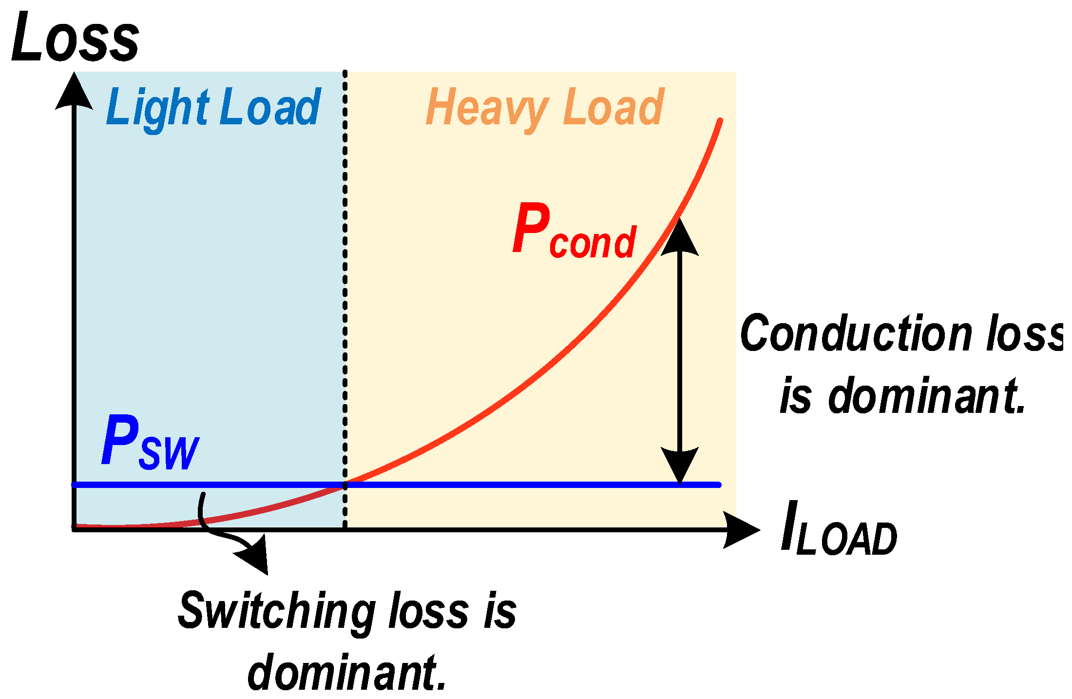
In the SI converter, there are two representative power losses, as shown in Figure 1. One is the switching loss (PSW) which is proportional to the switching frequency. When the switching frequency is fixed, the PSW is a constant independent of the ILOAD. The other is the conduction loss (Pcond). Since the Pcond is proportional to the square of the current, the Pcond is dominant in heavy load conditions. Therefore, reducing Pcond is important for improving power efficiency when ILOAD is large.
However, due to a large inductor current (iL), under heavy load conditions, these efficient SI converters also suffer from significant conduction loss (PDCR) dissipated at a parasitic DC resistance (RDCR) of a small inductor for size-limited mobile devices as shown in Figure 2. This large PDCR causes a severe thermal problem as well as low power efficiency in heavy load conditions. PDCR is expressed as follows:
where iL,RMS, IL, and ΔiL are the root-mean-square value, the DC value, and the ripple of the iL, respectively. Since the small inductor for the miniaturized mobile device can have much larger RDCR than the on-resistance of switches, reducing PDCR can achieve a significant improvement in power efficiency. To minimize the PDCR, reducing iL,RMS is the only solution when a large RDCR of the small inductor is used as shown in Equation (1). In particular, as the inductor with larger RDCR than the on-resistance of the switch is adopted, the efficiency improvement due to low iL,RMS is significantly increased.
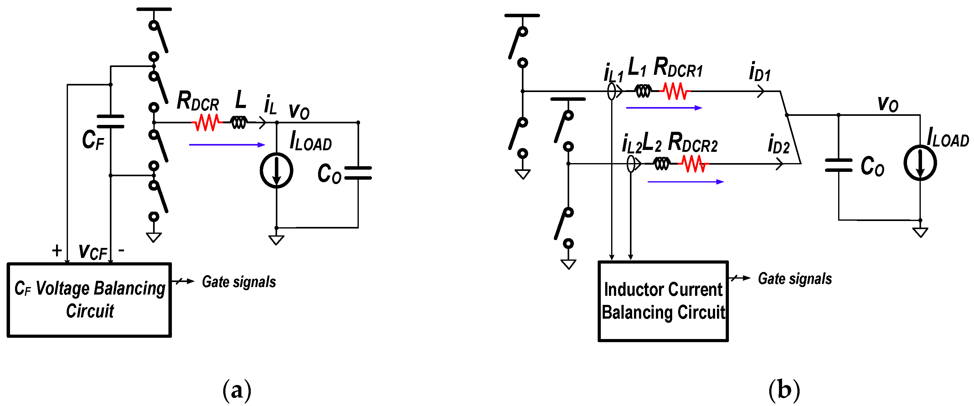
There are some alternative topologies that can reduce iL,RMS in a SI converter. For example, Figure 3a shows a multi-level structure with an additional flying capacitor that reduces ΔiL, thereby improving power efficiency in light or medium load conditions [17,18]. However, under heavy loads, since IL is much larger than ΔiL, the reduction of PDCR is limited. Alternatively, Figure 3b shows a multi-phase structure that can reduce IL and can result in increased power efficiency compared with the multi-level structure in heavy load conditions. However, it requires an additional inductor that is larger and more expensive than other passive components [19,20,21]. Furthermore, both the multi-level and the multi-phase structures require complex balancing circuits, as shown in Figure 3.
To resolve these issues, this paper proposes and analyzes a new type of hybrid switched inductor capacitor (SIC) converter with energy transfer media (ETM) using an additional flying capacitor. The topologies with the ETM provide improved efficiency by lowering IL owing to an additional current path in heavy load conditions.
The topologies with the proposed ETM are introduced in Section 2. In Section 3 and Section 4, the operation principle and a detailed conduction loss analysis of both the buck and buck-boost topologies are provided. In Section 5, different examples of extension to other topologies are explained and discussed. The simulation results for verification are presented in Section 6. Finally, a brief concluding summary is given in Section 7.
2. Energy Transfer Media
A hybrid SIC converter that possesses the advantages of both a SC converter and a SI converter is an attractive solution [22,23,24,25,26,27,28,29,30]. However, it is complicated to design because of the many complex combinations of power switches and flying capacitors. Also, various factors such as conversion ratios, balancing circuits, and power loss should be considered. To make it easy to design, and to reduce PDCR at the same time, this paper proposes an ETM that can be easily implemented with all types of non-isolated converters, such as buck, boost, and buck-boost topologies, with high efficiency under heavy load conditions. An ETM has been used previously to reduce only ΔiL [29,30]. However, similar to a multi-level converter, this structure is not effective at improving power efficiency under heavy load conditions. Therefore, we propose an ETM that uses an additional flying capacitor to obtain high efficiency in heavy load conditions, as shown in Figure 4.
The ETM uses one external flying capacitor (CF) and three power switches (SM1–SM3). This approach offers the advantage of inserting the capacitor current path into the output current path (C-path) as well as the inductor current path (L-path). This ETM with dual current paths can be applied to conventional non-isolated topologies by simply cascading the ETM, as shown in Figure 5. Figure 5a is a conceptual structure showing that the ETM can be applied to conventional converter topologies. Figure 5b–d show examples of applying the ETM to buck, boost, and buck-boost converters, respectively. This paper analyzes buck type and buck-boost type topologies with ETMs as examples and discusses possible extensions to other topologies.
3. Buck Converter with Energy Transfer Media
Figure 5b shows a buck converter with ETM (BKETM), which is composed of power switches S1–S2 and SM1–SM3, one inductor (L), one flying capacitor (CF), and one output capacitor (CO). The BKETM uses two operating modes (Φ1, Φ2), as shown in Figure 6a. The operation waveforms of the BKETM are shown in Figure 6b.
In Φ1, S1 and SM2 are turned on, and S2, SM1, and SM3 are turned off. At this time, iL is built up with a slope of 2(VIN − VO)/L and is delivered to the output. In Φ2, S2, SM1, and SM3 are turned on, and S1 and SM2 are turned off. While iL is de-energized with a slope of −VO/L, it is also delivered to the output. In the meantime, the capacitor current iC of CF flows to the output, while the voltage of CF is charged to VIN − VO. To derive a conversion ratio (MBK), applying the voltage sec balance to the inductor with duty cycle D is expressed as follows:
Simplifying Equation (2), MBK is given by:
The MBK of the BKETM from Equation (3) has a value between 0 and 1 as D varies from 0 to 1, which is the same as the range of a conventional buck converter (CBK). Therefore, in spite of the SIC converter, the BKETM behaves like a CBK without the limit of the conversion ratio.
To obtain the average value of the C-path current (IC,Φ2) delivered to the output in Φ2, we also apply charge balance to CF as shown below:
Simplifying Equation (4), IC,Φ2 is given by
Applying the charge balance to the output capacitor CO,
Substituting Equation (5) into Equation (6), IL can be expressed with ILOAD as shown below:
For the CBK, IL is always the same as ILOAD [3,4,13,14,15,16]. In contrast, for the proposed BKETM, IL is ILOAD divided by (1 + D). As MBK increases, IL decreases. Therefore, IL always has a smaller value than ILOAD due to the two current paths (L-path and C-path). As IL decreases, PDCR also is reduced compared to that of the CBK. To compare the total conduction loss with that of the CBK, we assume that since the parasitic resistance (RESR) of the flying capacitors is typically much smaller than other resistances, the loss of RESR can be ignored for simplicity. Also, the on-resistance of each switch is assumed to be the same as RON. Thus, the total conduction loss (Pcond,CBK) of the CBK is expressed as follows:
On the other hand, the total conduction loss (Pcond,BKETM) of the BKETM is as follows:
For the relative comparison with CBK, the ratio between Pcond,CBK and Pcond,BKETM is expressed as:
Figure 7 depicts the value calculated by Equation (13) versus the conversion ratio MBK for different RDCR. It shows that Pcond,BKETM is lower than Pcond,CBK across a wide range of MBK values. As described by Equation (7), the total conduction loss decreases because IL is reduced as MBK increases. Also, the larger the RDCR, the lower the Pcond,BKETM is compared with Pcond,CBK. Therefore, BKETM is a useful topology for step-down when a small inductor with a large RDCR is used in heavy load conditions.
4. Buck-Boost Converter with Energy Transfer Media
Since the boost converter with the ETM shown in Figure 5c has been previously described in detail in [27], this paper focuses on the buck-boost converter with ETM (BBETM) shown in Figure 5d. It is composed of power switches S1–S4, SM1–SM3, one inductor (L), one flying capacitor (CF), and one output capacitor (CO). The BBETM also uses two operating modes (Φ1, Φ2), as shown in Figure 8a. Its operation waveforms are shown in Figure 8b.
In Φ1, S1 and S3 are turned on while iL increases with a slope of VIN/L and is delivered to the output. At the same time, SM1 and SM3 turn on, and iC flows to the output through the C-path, while the voltage of CF is charged to VIN − VO. With a conventional buck-boost (CBB) converter, current cannot be delivered to the output while iL is building up. The ability of the BBETM to transfer the energy to the output during iL build-up is one of the main differences between the BBETM and a CBB converter. Owing to this operation, the output delivery current (iD) in the BBETM is continuous, resulting in a small output voltage ripple (∆VO). In Φ2, S2, SM2, and SM3 turn on, and iL is delivered to the output.
For the BBETM conversion ratio (MBB), applying the voltage sec balance to the inductor based on the operation is expressed as follows:
Simplifying Equation (14), MBB is given by:
MBB of the BBETM from Equation (15) has a value between 0.5 and infinity as D varies from 0 to 1. This means that the BBETM can operate for step-up and step-down output voltages. Since the conversion ratio is limited to less than 0.5, this approach is not appropriate for applications with a low conversion ratio. However, it offers several advantages compared with a CBB converter.
First, similar to the buck type converter, the BBETM IL is reduced compared with that of a CBB converter. To analyze this, the average value of the C-path current (IC,Φ1) in Φ1 can be obtained by applying charge balance to the CF as shown below:
Simplifying Equation (16), IC,Φ1 is given by
Applying the charge balance to CO,
Substituting Equation (17) into Equation (18), IL can be expressed with load current (ILOAD) as shown below:
Due to the two current paths in the ETM, the BBETM IL is as low as MBBILOAD, while the CBB IL is (1 + MBB) ILOAD [4]. Therefore, the BBETM PDCR can be reduced. To compare the total conduction loss with that of the CBB, the on-resistance of each switch is assumed to be the same as RON, and the total conduction loss (Pcond,CBB) of the CBB is expressed as follows:
In contrast, the total conduction loss (Pcond,BBETM) of the BBETM is expressed as
For the relative comparison with the CBB, the ratio between Pcond,CBB and Pcond,BBETM for the BBETM is expressed as
Figure 9 depicts the values of Equation (24) versus the conversion ratio MBB for different RDCR values, showing that the Pcond,BBETM is lower than the Pcond,CBB for a wide range of MBB values. This finding demonstrates that the BBETM is more efficient than CBB due to the dual current paths. Also, it shows that the larger the RDCR, the lower Pcond,BBETM is, compared with Pcond,CBB. Therefore, the BBETM is useful for step-up and step-down applications when a small inductor with a large RDCR is used in heavy load conditions.
5. Extension to Other Topologies
5.1. Multi-Phase Buck Converter with ETM
The multi-phase converter is a structure that allows multiple inductors to transfer energy to the output when it is difficult to support sufficient energy for the output with only a single converter. The proposed ETM can also easily implement a SIC converter with a multi-phase structure. As shown in Figure 10a, the multi-phase buck converter can be designed with two ETMs for a single output with heavy ILOAD. The proposed multi-phase buck converter with ETM (MBKETM) consists of one inductor and two flying capacitors, because two ETMs are used. Figure 10b shows the operation principle of the MBKETM. The advantage of the MBKETM over other topologies with an ETM is that the input frequency (fIN) for the input duty (Φ1, Φ2) and the output switching frequency (fOUT) for the output duty (ΦO1, ΦO2) can be independently controlled. As an example, in this paper, the input duty is controlled to regulate the output voltage, and the output duty is always fixed at 0.5 so that the C-path currents (IC,ΦO1, IC,ΦO2) can be maintained at the inductor current IL. Then, applying charge balance to the output capacitor CO in this condition,
From Equation (25), IL can also be maintained at half of ILOAD, the same value as IL of the conventional multi-phase buck converter (CMBK) with two inductors [19]. Thus, the MBKETM can generate triple current paths (one L-path, two C-paths) with a single inductor and two low-cost, small flying capacitors, thus reducing cost and size compared with a CMBK. Moreover, owing to these triple current paths, the ripple of the output delivery current iD is reduced such that the output voltage ripple ∆VO is smaller than that of the BKETM. Furthermore, by adopting a higher output frequency (fOUT) for the output duty (ΦO1, ΦO2) than the input frequency (fIN) for the input duty (Φ1, Φ2), ∆VO can be further reduced. These characteristics are verified with simulation results in the next section.
5.2. Single-Inductor Multiple-Output Buck Converter with ETM
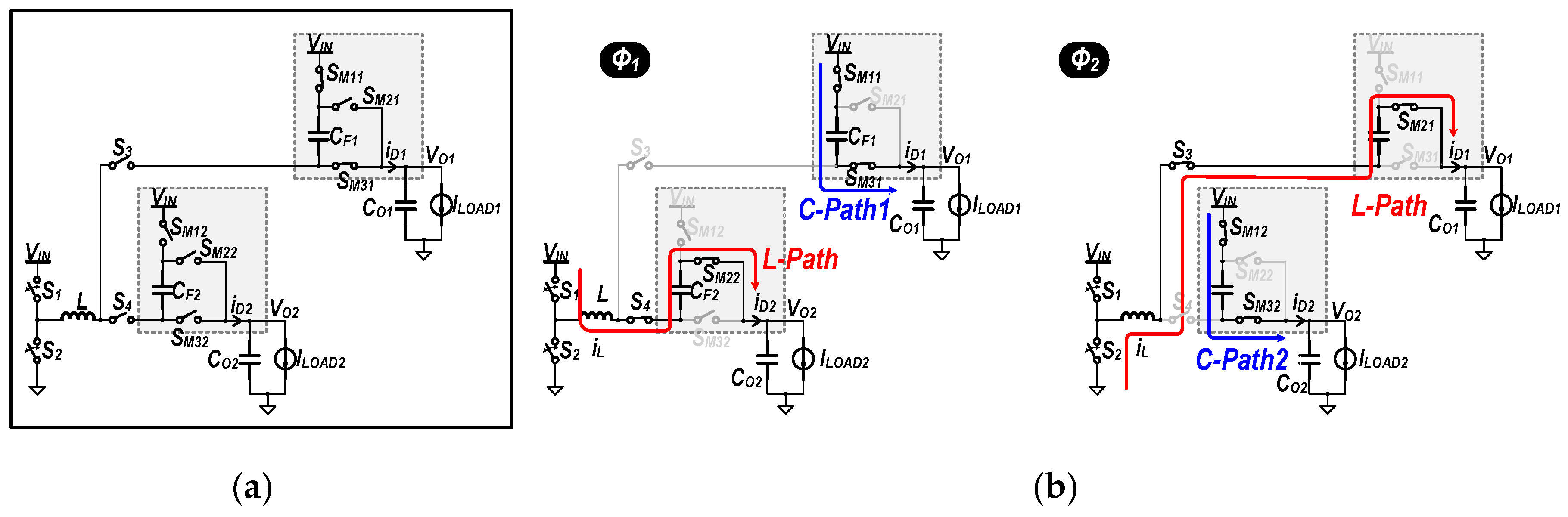
As the name suggests, a single-inductor multiple-output (SIMO) converter can regulate many outputs with one inductor [31,32,33]. As shown in Figure 11a as an example, it is also easy to make a dual-output structure with two ETMs. More outputs can be generated by increasing the number of ETMs. Figure 11b shows the operation of a single-inductor dual-output (SIDO) buck converter with two ETMs (SIDOETM). Because of the ETMs, IL is reduced compared with that of a conventional SIMO converter (CSIMO). Moreover, since the SIDOETM has triple paths (one L-path and two C-paths), the currents (iD1, iD2) delivered to each output (VO1, VO2) are continuous. In contrast, with the CSIMO, the currents delivered to the output are discontinuous because a single inductor must be used to distribute the energy to each output during different time slots. Therefore, the CSIMO has the disadvantage of significant large voltage ripple at each output. In contrast, since the proposed SIDOETM has continuous iD1 and iD2, the output voltage ripples (∆VO1, ∆VO2) can be significantly reduced. Also, the CSIMO typically uses a comparator-based control for regulation of the outputs, which is very vulnerable to spike noise at the outputs [32,33]. Because the discontinuous output delivery currents can generate large spikes at every output due to the parasitic inductance that is connected to the output capacitors in series, it can cause a malfunction on the regulation control of the CSIMO. Therefore, the SIDOETM has an additional advantage of being able to alleviate the spike noise due to continuous output delivery current.
6. Simulation Results and Discussion
6.1. Buck Converter with ETM
Table 1 shows the simulation conditions for the proposed BKETM. To obtain accurate simulation results, the switching loss model is included as well as the conduction loss in the simulation. Cgate and Coss in Table 1 are the gate capacitance and the output capacitance of the power switch, respectively, for considering the switching loss. Figure 12 shows the simulated waveforms to confirm the operation of the converter.
The results show a IL of 720 mA, lower than the ILOAD of 1 A. Also, the charge balance of the capacitor is satisfied through ic, and the voltage and current values of each node match the calculation in Section 3. Owing to the lowered IL, high efficiency can be achieved even when using a small inductor, reducing PDCR. This type of converter can also solve the heat problems associated with high performance mobile devices. However, since the BKETM has a pulsating iD due to the C-path, a large ∆VO of 35 mV is observed, as shown in Figure 12.
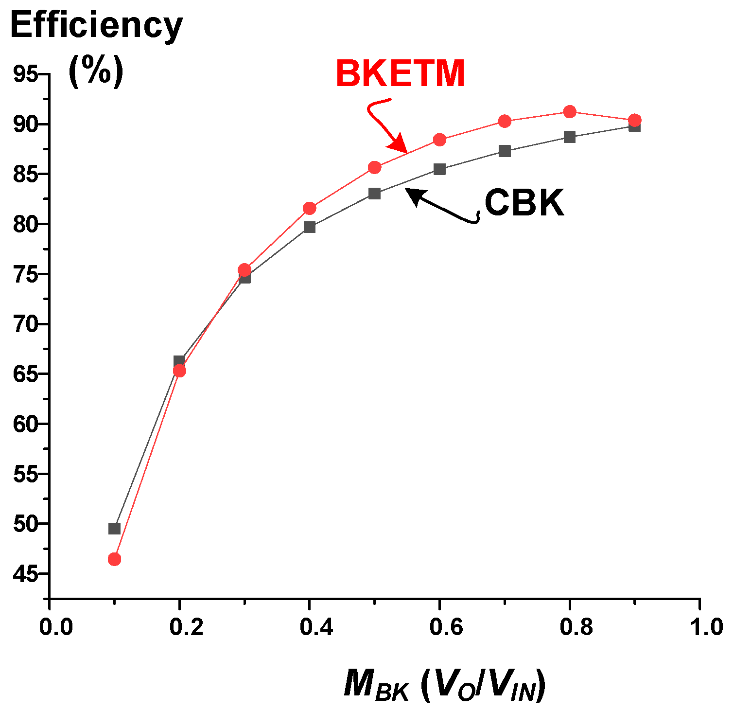
Figure 13 shows the simulated efficiency plots for both the BKETM and CBK with different conversion ratios (MBK). From Equation (7), the larger the value of MBK, the larger the reduction in IL. Thus, the efficiency of the BKETM is higher than that of the CBK when MBK is high. However, as MBK approaches 1, the C-path current, IC,Φ2, rapidly increases according to Equation (5). Then, the total conduction loss increases again, resulting in the degradation of the efficiency of the BKETM.
Figure 14 shows the efficiency plots with different values of ILOAD when MBK is 0.6 or 0.3. When MBK is high, as ILOAD increases, the efficiency improves compared with that of the CBK. However, when MBK is low, the reduction effect of IL is not significant. Then, even if ILOAD becomes large, the increment in efficiency is negligible. Therefore, the BKETM is an efficient topology when MBK is high under heavy load conditions.
6.2. Buck-Boost Converter with ETM
Table 2 shows the simulation conditions for the proposed BBETM. Figure 15 shows the simulation results to confirm the operation of the converter.
The simulation results show that the BBETM achieves a lower IL (1.2 A) than that of the CBB (2.2 A). Also, the charge balance of CF is satisfied through ic, and the voltage and current values of each node are matched with the calculation in Section 4. Due to reduced inductor current, the conduction loss can be decreased even when a small inductor is used. Moreover, in contrast to the CBB iD, the BBTEM iD is continuous due to the addition of the C-path, resulting in a smaller ∆VO of 25 mV compared with the 130 mV observed for the CBB under the same operating conditions, as shown in Figure 16.
Figure 17 shows the simulated efficiency plots for both the BBETM and CBB with different conversion ratio values, MBB. The BBETM has a much higher efficiency than the CBB across a wide range of MBB values because the buck-boost topology generates a much larger IL than the buck-type topology due to a structural characteristic.
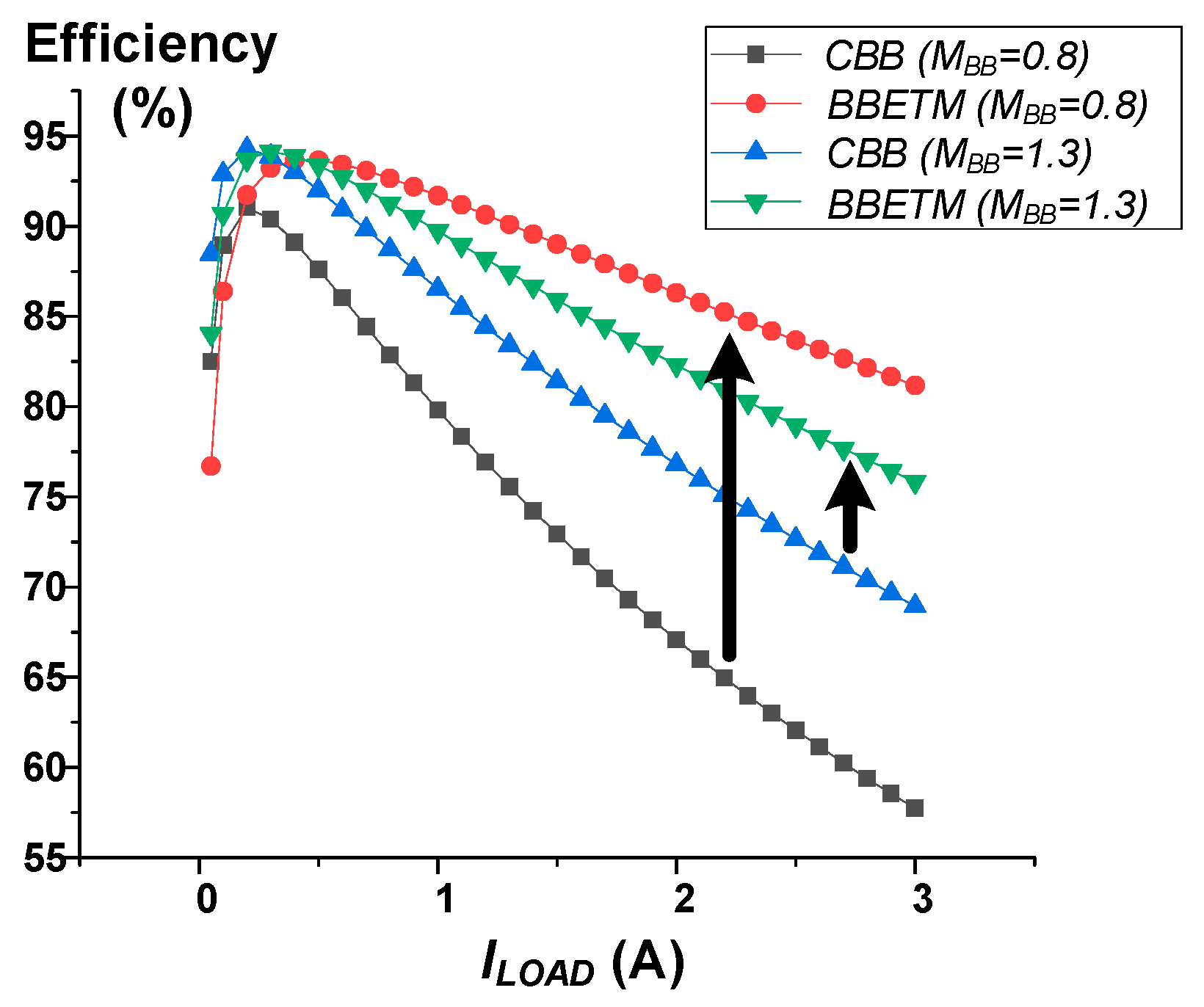
Figure 18 shows the efficiency plots with different ILOAD values when MBB is 0.8 or 1.3. Based on Equation (19), a lower MBB is associated with a larger reduction in IL for the BBETM compared to the CBB. Thus, with a low MBB, as ILOAD increases, the increment in efficiency for BBETM compared with CBB becomes significant.
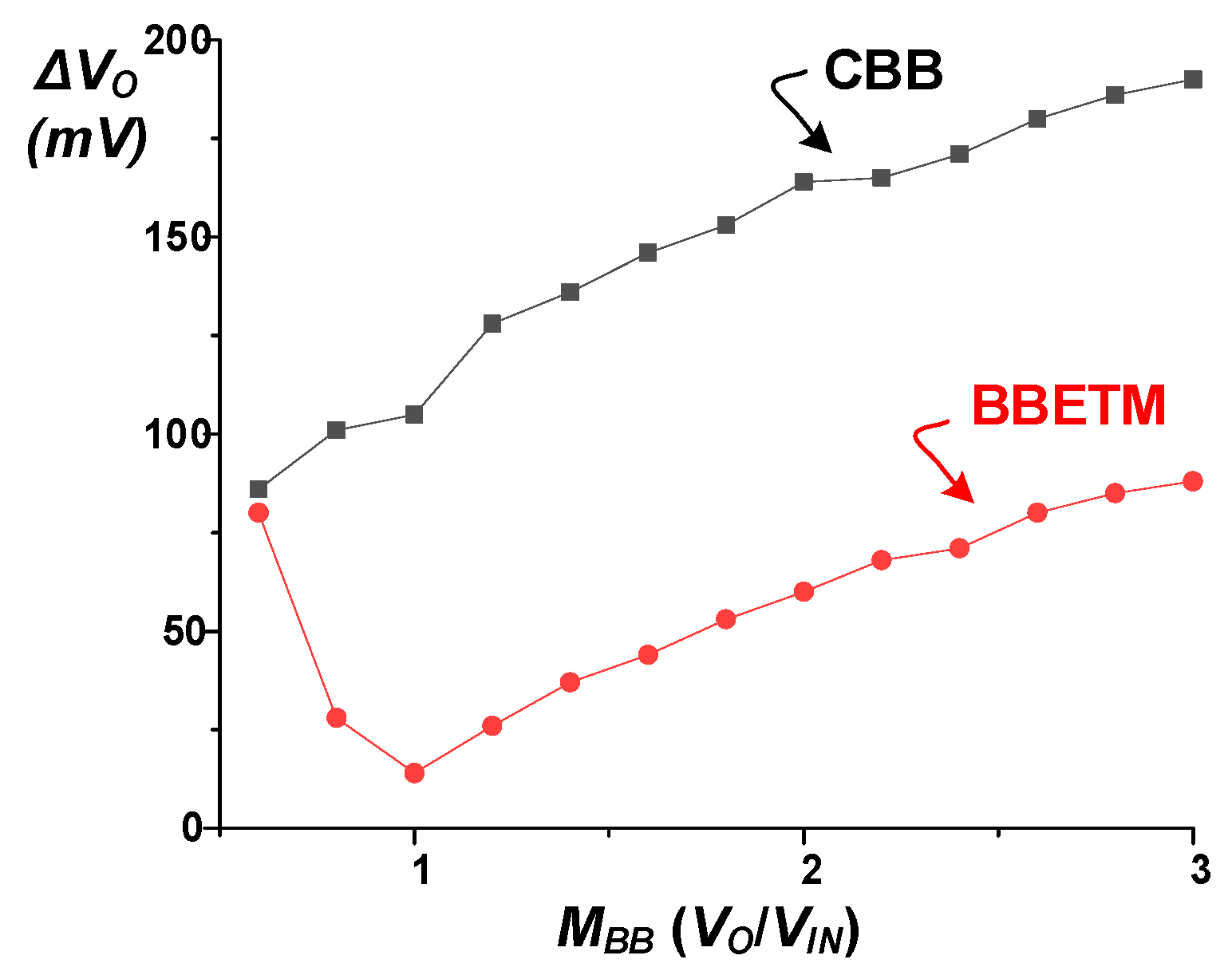
The BBETM has another benefit of a small ∆VO. Figure 19 is a plot comparing the ∆VO of the proposed BBETM and the CBB under the same operating conditions. The BBETM ∆VO is lower than that of the CBB across a wide range of MBB values. However, when MBB is very low, which means there is a small duty cycle D, the C-path current rapidly increases as shown in Equation (17), resulting in a large ∆VO again.
6.3. Multi-Phase Buck Converter with ETM
The MBKETM is simulated under the operating conditions as shown in Table 3.
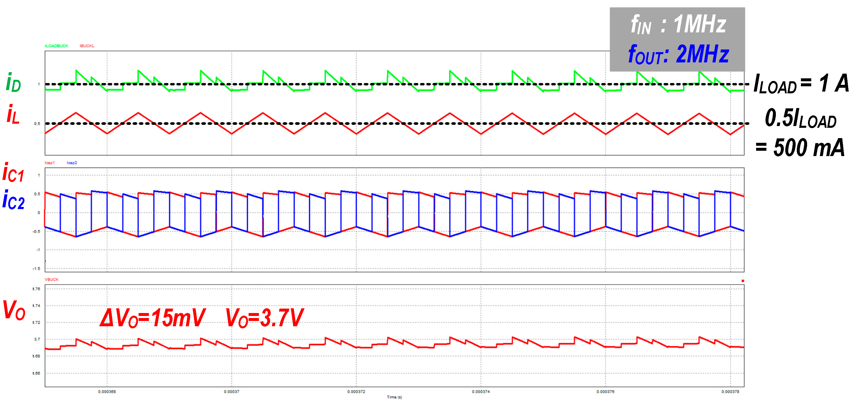
It is possible to separate fIN and fOUT as mentioned in Section 5. Figure 20, Figure 21 and Figure 22 show the simulation waveforms of the MBKETM with different values of fOUT. Figure 20 shows the waveforms when fIN and fOUT are both equal to 1 MHz. IL is reduced to half of ILOAD because the output duty is fixed at 0.5, as shown in Equation (25). Moreover, ∆VO is as small as 25 mV because iD is continuous due to the presence of both the L-path and the C-path. Figure 21 shows the waveforms when fOUT is two times higher than fIN. Under these conditions, ∆VO is further reduced to 15 mV because the effective frequency seen at the output is increased. Figure 22 shows the waveforms when fOUT is triple the value of fIN. Under these conditions, ∆VO is further reduced to 10 mV. However, since high fOUT can increase the switching loss in the converter, causing degradation of efficiency, there is a trade-off between ∆VO and power efficiency.
In summary, the proposed MBKETM, using one inductor and two flying capacitors, achieves a similar reduction of IL to half of ILOAD as the CMBK does with two large, expensive inductors, thereby reducing PDCR significantly. Furthermore, because fIN and fOUT can be controlled independently, ∆VO can be further reduced. Also, unlike the CMBK, the proposed MBKETM does not require a complex current balancing controller in spite of the multi-phase operation.
6.4. Single-Inductor Multiple-Output Buck Converter with ETM
Table 4 shows the simulation conditions of the proposed SIDOETM. Figure 23 shows the simulated iL, iC1, iC2, iD1, and iD2 of the proposed converter. Due to the dual current paths, IL is lower than the sum of ILOAD1 and ILOAD2.
Moreover, since iD1 and iD2 do not drop to zero, the continuous current (iD1, iD2) flows to the respective output (VO1, VO2). Figure 24 shows that the output voltage is well regulated to 2.8 V and 2 V. The ripples of each output are 15 mV and 13 mV, respectively. It has a lower ∆VO than the CSIMO [31,32,33].
Table 5 and Table 6 summarize the advantages of the proposed topologies with the ETM. The common advantage is the reduction of IL, resulting in low total conduction loss in heavy load conditions. Moreover, unlike conventional topologies that have discontinuous iD, such as the CBB and CSIMO topologies, the proposed ETM topologies have very low ∆VO because of the continuous iD. The MBKETM can control fIN and fOUT independently, resulting in further reduction of ∆VO.
7. Conclusions
In this paper, an ETM was proposed to make a promising hybrid switched inductor capacitor converter easier to design for heavy load conditions. New topologies with ETM, which generate dual current paths, were analyzed and compared with conventional topologies that have a single current path. Owing to the dual current paths (L-path and C-path), all of the topologies with the ETM shared the common advantage of reduced inductor current. Since it significantly decreases conduction loss dissipated at a considerable parasitic DC resistance of the inductor, the heating issue can be resolved at the same time as the power efficiency is improved, which was discussed with buck and buck-boost converters with ETMs as examples. Moreover, the buck-boost converter with ETM has continuous output delivery current, resulting in much smaller output voltage ripple than that of a conventional buck-boost converter. Also, a multi-phase converter and single-inductor multiple-output converter with several ETMs were proposed and simulated. The multi-phase converter with ETM offered the additional advantage of separating the switching frequency between the input frequency and the output frequency to further reduce the output ripple voltage. Additionally, the SIMO converter with ETM achieved a small output voltage ripple, similar to that of a buck-boost converter with ETM, due to the continuous output delivery current. In summary, the ETM can be implemented easily by combining with conventional topologies, and it has several merits such as reduced inductor current, small output voltage ripple, and independent frequency control. The proposed ETM can be applied to various non-isolated topologies as a promising solution for use in heavy load conditions with a small inductor.
Funding
This research received no external funding.
Conflicts of Interest
The author declares no conflicts of interest.
References
- Carroll, A.; Heiser, G. An analysis of power consumption in a smartphone. In Proceedings of the 2010 USENIX Conference on USENIX Annual Technical Conference, Boston, MA, USA, 23–25 June 2010. [Google Scholar]
- Lee, I.; Lee, Y.; Sylvester, D.; Blaauw, D. Battery Voltage Supervisors for Miniature IoT Systems. IEEE J. Solid-State Circuits 2016, 51, 2743–2756. [Google Scholar] [CrossRef]
- Hella, M.M.; Mercier, P.P. Power Management Integrated Circuits, 1st ed.; CRC Press Publishers: Boca Raton, FL, USA, 2016. [Google Scholar]
- Erickson, R.W.; Maksimovi’c, D. Fundamentals of Power Electronics, 2nd ed.; Kluwer Academic Publishers: Norwell, MA, USA, 2001. [Google Scholar]
- Park, J.; Ko, W.-J.; Kang, D.-S.; Lee, Y.; Chun, J.-H. An Output Capacitor-Less Low-Dropout Regulator with 0–100 mA Wide Load Current Range. Energies 2019, 12, 211. [Google Scholar] [CrossRef]
- Hazucha, P.; Karnik, T.; Bloechel, B.A.; Parsons, C.; Finan, D.; Borkar, S. Area-Efficient Linear Regulator with Ultra-Fast Load Regulation. IEEE J. Solid-State Circuits 2005, 40, 933–940. [Google Scholar] [CrossRef]
- Milliken, R.J.; Silva-Martinez, J.; Sanchez-Sinencio, E. Full On-Chip CMOS Low-Dropout Voltage Regulator. IEEE Trans. Circuits Syst. I 2007, 54, 1879–1890. [Google Scholar] [CrossRef] [Green Version]
- Guo, J.; Leung, K.N. A 6-_WChip-Area-Efficient Output-Capacitorless LDO in 90-nm CMOS Technology. IEEE J. Solid-State Circuits 2010, 45, 1896–1905. [Google Scholar] [CrossRef]
- Seeman, M.D.; Sanders, S.R. Analysis and optimization of switched-capacitor DC-DC converters. IEEE Trans. Power Electron. 2008, 23, 841–851. [Google Scholar] [CrossRef]
- Le, H.P.; Sanders, S.R.; Alon, E. Design Technique for fully integrated Switched-Capacitor DC-DC Converters. IEEE J. Solid-State Circuits 2011, 46, 2120–2131. [Google Scholar] [CrossRef]
- Bang, S.; Blaauw, D.; Sylvester, D. A Successive-Approximation Switched-Capacitor DC–DC Converter with Resolution of VIN/2N for a Wide Range of Input and Output Voltages. IEEE J. Solid-State Circuits 2016, 51, 543–556. [Google Scholar]
- Saif, H.; Lee, Y.; Lee, H.; Kim, M.; Khan, M.B.; Chun, J.-H.; Lee, Y. A Wide Load Current and Voltage Range Switched Capacitor DC–DC Converter with Load Dependent Configurability for Dynamic Voltage Implementation in Miniature Sensors. Energies 2018, 11, 3092. [Google Scholar] [CrossRef]
- Chiang, C.; Chen, C. Zero-Voltage-Switching Control for a PWM Buck Converter Under DCM/CCM Boundary. IEEE Trans. Power Electron. 2009, 24, 2120–2212. [Google Scholar] [CrossRef]
- Suh, J.; Seok, J.; Kong, B. A Fast Response PWM Buck Converter with Active Ramp Tracking Control in Load Transient period. IEEE Trans. Circuits Syst. II Express Briefs 2018, 66, 467–471. [Google Scholar] [CrossRef]
- Calderón, A.; Vinagre, B.; Feliu, V. Fractional order control strategies for power electronic buck converters. Signal Process. 2006, 86, 2803–2819. [Google Scholar] [CrossRef]
- Suh, J.-D.; Yun, Y.-H.; Kong, B.-S. High-Efficiency DC–DC Converter with Charge-Recycling Gate-Voltage Swing Control. Energies 2019, 12, 899. [Google Scholar] [CrossRef]
- Abdulslam, A.; Mohammad, B.; Ismail, M.; Mercier, P.; Ismail, Y. A 93% Peak Efficiency Fully-Integrated Multilevel Multistate Hybrid DC–DC Converter. IEEE Trans. Circuits Syst. I 2018, 65, 2617–2630. [Google Scholar] [CrossRef]
- Kim, W.; Brooks, D.; Wei, G.-Y. A fully-integrated 3-level DC-DC converter for nanosecond-scale DVSF. IEEE J. Solid-State Circuits 2012, 47, 206–219. [Google Scholar] [CrossRef]
- Li, P.; Xue, L.; Hazucha, P.; Karnik, T.; Bashirullah, R. A delay-locked loop synchronization scheme for high-frequency multiphase hysteretic DC-DC converters. IEEE J. Solid-State Circuits 2009, 44, 3131–3145. [Google Scholar] [CrossRef]
- Abedinpour, S.; Bakkaloglu, B.; Kiaei, S. A Multistage Interleaved Synchronous Buck Converter with Integrated Output Filter in 0.18µm SiGe Process. IEEE Trans. Power Electron. 2007, 22, 2164–2175. [Google Scholar] [CrossRef]
- Huang, C.; Mok, P.K.T. A 100 MHz 82.4% Efficiency Package-Bondwire Based Four-Phase Fully-Integrated Buck Converter with Flying Capacitor for Area Reduction. IEEE J. Solid-State Circuits 2013, 48, 2977–2988. [Google Scholar] [CrossRef]
- Rodiˇc, M.; Milanoviˇc, M.; Truntiˇc, M.; Ošlaj, B. Switched-Capacitor Boost Converter for Low Power Energy Harvesting Applications. Energies 2018, 11, 3156. [Google Scholar] [CrossRef]
- Tran, V.-T.; Nguyen, M.-K.; Choi, Y.-O.; Cho, G.-B. Switched-Capacitor-Based High Boost DC-DC Converter. Energies 2018, 11, 987. [Google Scholar] [CrossRef]
- Ju, Y.; Shin, S.; Huh, Y.; Park, S.; Bang, J.; Kim, K.; Choi, S.; Lee, J.; Cho, G. A hybrid inductor-based flying-capacitor-assisted step-up/step-down DC-DC converter with 96.56% efficiency. In Proceedings of the 2017 IEEE International Solid-State Circuits Conference (ISSCC), San Francisco, CA, USA, 5–9 February 2017; pp. 184–185. [Google Scholar]
- Liu, W.; Assem, P.; Lei, Y.; Hanumolu, P.K.; Pilawa-Podgurski, R. A 94.2%-peak-efficiency 1.53A direct-battery-hook-up hybrid Dickson switched-capacitor DC-DC converter with wide continuous conversion ratio in 65nm CMOS. In Proceedings of the 2017 IEEE International Solid-State Circuits Conference (ISSCC), San Francisco, CA, USA, 5–9 February 2017; pp. 182–183. [Google Scholar]
- Ko, M.; Kim, K.; Woo, Y.; Shin, S.; Han, H.; Huh, Y.; Kang, G.; Cho, J.; Lim, S.; Park, S.; et al. A 97% high-efficiency 6μs fast-recovery-time buck-based step-up/down converter with embedded 1/2 and 3/2 charge-pumps for li-lon battery management. In Proceedings of the 2018 IEEE International Solid-State Circuits Conference (ISSCC), San Francisco, CA, USA, 11–15 February 2018; pp. 428–430. [Google Scholar]
- Shin, S.; Huh, Y.; Ju, Y.; Choi, S.; Shin, C.; Woo, Y.; Choi, M.; Park, S.; Sohn, Y.; Ko, M.; et al. A 95.2% efficiency dual-path DC-DC step-up converter with continuous output current delivery and low voltage ripple. In Proceedings of the 2018 IEEE International Solid-State Circuits Conference (ISSCC), San Francisco, CA, USA, 11–15 February 2018; pp. 430–432. [Google Scholar]
- Huh, Y.; Shin, S.; Hong, S.; Woo, Y.; Ju, Y.; Choi, S.; Cho, G. A Hybrid Dual-Path Step-Down Converter with 96.2% Peak Efficiency Using a 250mΩ Large-DCR Inductor. In Proceedings of the 2018 IEEE Symposium on VLSI Circuits, Honolulu, HI, USA, 18–22 June 2018; pp. 225–226. [Google Scholar]
- Wang, S.; Woo, Y.; Yuk, Y.; Lee, B.; Cho, G.; Cho, G. Efficiency enhanced Single-Inductor Boost-Inverting Flyback converter with Dual Hybrid Energy transfer media and a Bifurcation Free Comparator. In Proceedings of the 2010 Proceedings of ESSCIRC, Seville, Spain, 14–16 September 2010; pp. 450–453. [Google Scholar]
- Wang, S.; Woo, Y.; Yuk, Y.; Cho, G.; Cho, G. High efficiency Single-Inductor Boost/Buck Inverting Flyback converter with hybrid energy transfer media and multi level gate driving for AMOLED panel. In Proceedings of the 2010 Symposium on VLSI Circuits, Honolulu, HI, USA, 16–18 June 2010; pp. 59–60. [Google Scholar]
- Dongsheng, M.; Wing-Hung, K.; Chi-Ying, T. A pseudo-CCM/DCM SIMO switching converter with freewheel switching. IEEE J. Solid-State Circuits 2003, 38, 1007–1014. [Google Scholar] [CrossRef] [Green Version]
- Lu, D.; Qian, Y.; Hong, Z. 4.3 An 87%-peak-efficiency DVS-capable single-inductor 4-output DC-DC buck converter with ripple-based adaptive off-time control. In Proceedings of the 2014 IEEE International Solid-State Circuits Conference Digest of Technical Papers (ISSCC), San Francisco, CA, USA, 9–13 February 2014; pp. 82–83. [Google Scholar]
- Goh, T.Y.; Ng, W.T. Single Discharge Control for Single-Inductor Multiple-Output DC–DC Buck Converters. IEEE Trans. Power Electron. 2018, 33, 2307–2316. [Google Scholar] [CrossRef]
Figure 1.
Graph of the switching loss and conduction loss in different conditions.

Figure 2.
Conduction loss of a parasitic DC resistance (RDCR) of the inductor in heavy load conditions.
Figure 2.
Conduction loss of a parasitic DC resistance (RDCR) of the inductor in heavy load conditions.

Figure 3.
Alternative topologies for reducing conduction loss in RDCR: (a) multi-level buck converter; (b) multi-phase buck converter.
Figure 3.
Alternative topologies for reducing conduction loss in RDCR: (a) multi-level buck converter; (b) multi-phase buck converter.

Figure 4.
Energy transfer media with a flying capacitor.

Figure 5.
(a) Conventional topology with an energy transfer media; (b) buck converter; (c) boost converter; (d) buck-boost converter.
Figure 5.
(a) Conventional topology with an energy transfer media; (b) buck converter; (c) boost converter; (d) buck-boost converter.
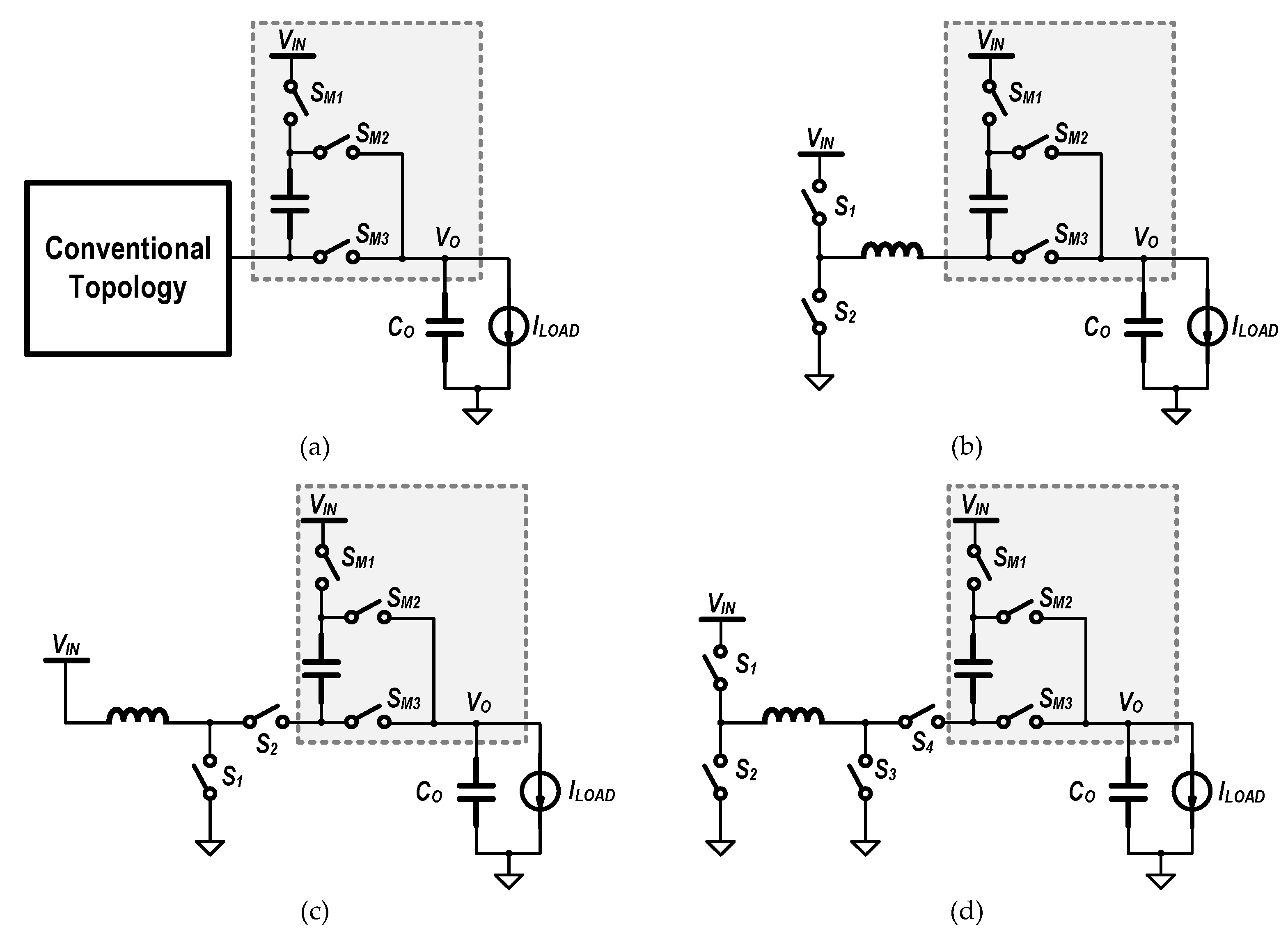
Figure 6.
Operating mode (a) and waveforms (b) of buck converter with energy transfer media (BKETM).
Figure 6.
Operating mode (a) and waveforms (b) of buck converter with energy transfer media (BKETM).
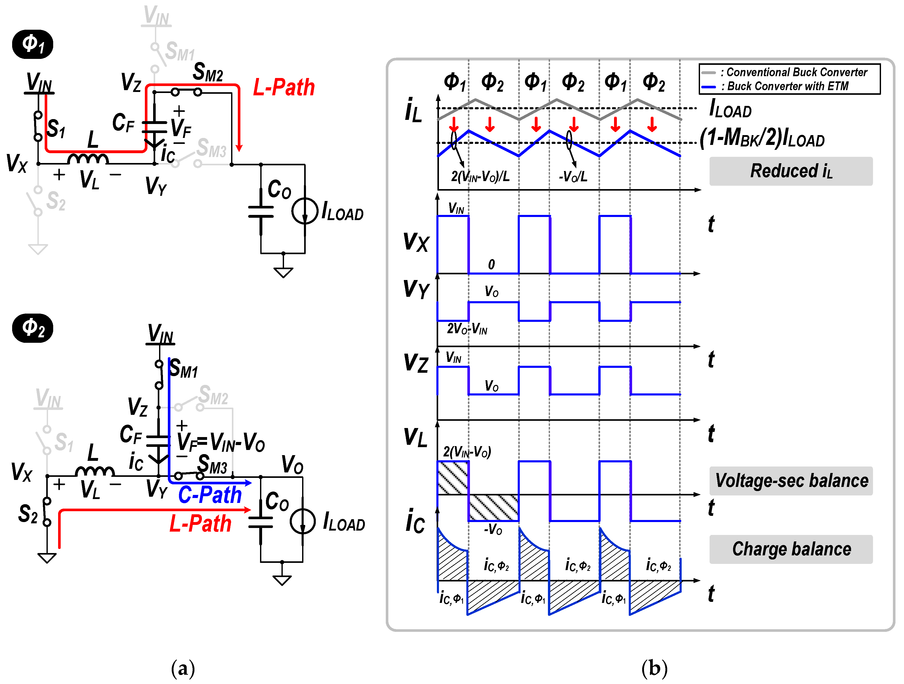
Figure 7.
Conduction loss comparison for the buck converter with energy transfer media (BKETM) and conventional buck converter (CBK) with different RDCR values.
Figure 7.
Conduction loss comparison for the buck converter with energy transfer media (BKETM) and conventional buck converter (CBK) with different RDCR values.

Figure 8.
Operating modes (a) and waveforms (b) of buck-boost converter with ETM.

Figure 9.
Conduction loss comparison of buck-boost converter with energy transfer media (BBETM) and conventional buck-boost (CBB) for different RDCR values.
Figure 9.
Conduction loss comparison of buck-boost converter with energy transfer media (BBETM) and conventional buck-boost (CBB) for different RDCR values.

Figure 10.
Topology (a) and operation (b) of a multi-phase buck converter with ETM.

Figure 11.
Topology (a) and operation (b) of a single-inductor dual-output buck converter with ETM.

Figure 12.
Simulation waveforms of a buck converter with ETM.

Figure 13.
Simulated efficiency plot of a buck converter with ETM at different conversion ratios.

Figure 14.
Simulated efficiency plot for a buck converter with ETM at different load currents.

Figure 15.
Simulation waveforms of buck-boost converter with ETM.

Figure 16.
Simulated output voltage ripple of BBETM compared with CBB.

Figure 17.
Simulated efficiency plot of a buck-boost converter with ETM at different conversion ratios.
Figure 17.
Simulated efficiency plot of a buck-boost converter with ETM at different conversion ratios.

Figure 18.
Simulated efficiency plot of a buck-boost converter with ETM at different load currents.

Figure 19.
Simulated output voltage ripple plot of the BBETM and CBB across different conversion ratios.
Figure 19.
Simulated output voltage ripple plot of the BBETM and CBB across different conversion ratios.

Figure 20.
Simulated waveforms of the multi-phase buck converter with energy transfer media (MBKETM) with fIN = 1 MHz and fOUT = 1 MHz.
Figure 20.
Simulated waveforms of the multi-phase buck converter with energy transfer media (MBKETM) with fIN = 1 MHz and fOUT = 1 MHz.

Figure 21.
Simulated waveforms of the MBKETM with fIN = 1 MHz and fOUT = 2 MHz.

Figure 22.
Simulated waveforms of the MBKETM with fIN = 1 MHz and fOUT = 3 MHz.

Figure 23.
Simulated current waveforms of the proposed single-inductor dual-output converter with ETM (SIDOETM).
Figure 23.
Simulated current waveforms of the proposed single-inductor dual-output converter with ETM (SIDOETM).

Figure 24.
Simulated voltage waveforms of the proposed SIDOETM.


Table 1.
Simulation conditions for buck converter with ETM.
| VIN | VOUT | ILOAD | fIN | L | RDCR |
| 5 V | 2.8 V | 1 A | 1 MHz | 4.7 μH | 0.2 Ω |
| CF | CO | RON | RESR | Cgate | Coss |
| 4.7 μF | 4.7 μF | 50 mΩ | 20 mΩ | 250 pF | 100 pF |
Table 2.
Simulation conditions for buck-boost converter with ETM.
| VIN | VOUT | ILOAD | fIN | L | RDCR |
| 5 V | 6 V | 1 A | 1 MHz | 4.7 μH | 0.2 Ω |
| CF | CO | RON | RESR | Cgate | Coss |
| 4.7 μF | 4.7 μF | 50 mΩ | 20 mΩ | 250 pF | 100 pF |
Table 3.
Simulation conditions for multi-phase buck converter with ETM.
| VIN | VOUT | ILOAD | fIN | L | RDCR |
| 5 V | 3.7 V | 1 A | 1 MHz | 4.7 μH | 0.2 Ω |
| CF | CO | RON | RESR | Cgate | Coss |
| 4.7 μF | 4.7 μF | 50 mΩ | 20 mΩ | 250 pF | 100 pF |
Table 4.
Simulation conditions for single-inductor multiple-output (SIDO) converter with ETM.
| VIN | VOUT1/VOUT2 | ILOAD1/ILOAD2 | fIN | L | RDCR |
| 5 V | 2.8 V/2 V | 0.7 A/0.5 A | 1 MHz | 4.7 μH | 0.2 Ω |
| CF | CO | RON | RESR | Cgate | Coss |
| 4.7 μF | 4.7 μF | 50 mΩ | 20 mΩ | 250 pF | 100 pF |
Table 5.
Summary table with buck and buck-boost type converters.
| Advantages | BKETM | CBK | BBETM | CBB |
|---|---|---|---|---|
| Reduction of IL | O | × | O | × |
| Reduction of ∆VO | × | × | O | × |
| Continuous iD | O | O | O | × |
O: Yes; ×: No.
Table 6.
Summary table with multi-phase buck and single-inductor dual-output (SIDO) buck type converters.
Table 6.
Summary table with multi-phase buck and single-inductor dual-output (SIDO) buck type converters.
| Advantages | MBKETM | CMBK | SIDOETM | CSIMO |
|---|---|---|---|---|
| Reduction of IL | O | × | O | × |
| Reduction of VO | O | × | O | × |
| Continuous iD | O | O | O | × |
| Separated frequency | O | × | × | × |
O: Yes; ×: No.
© 2019 by the author. Licensee MDPI, Basel, Switzerland. This article is an open access article distributed under the terms and conditions of the Creative Commons Attribution (CC BY) license (http://creativecommons.org/licenses/by/4.0/).
Share and Cite
MDPI and ACS Style
Shin, S.-U. An Analysis of Non-Isolated DC-DC Converter Topologies with Energy Transfer Media. Energies 2019, 12, 1468. https://doi.org/10.3390/en12081468
AMA Style
Shin S-U. An Analysis of Non-Isolated DC-DC Converter Topologies with Energy Transfer Media. Energies. 2019; 12(8):1468. https://doi.org/10.3390/en12081468
Chicago/Turabian StyleShin, Se-Un. 2019. "An Analysis of Non-Isolated DC-DC Converter Topologies with Energy Transfer Media" Energies 12, no. 8: 1468. https://doi.org/10.3390/en12081468
Note that from the first issue of 2016, this journal uses article numbers instead of page numbers. See further details here.