Design and Optimization of Three-Phase Dual-Active-Bridge Converters for Electric Vehicle Charging Stations


Abstract
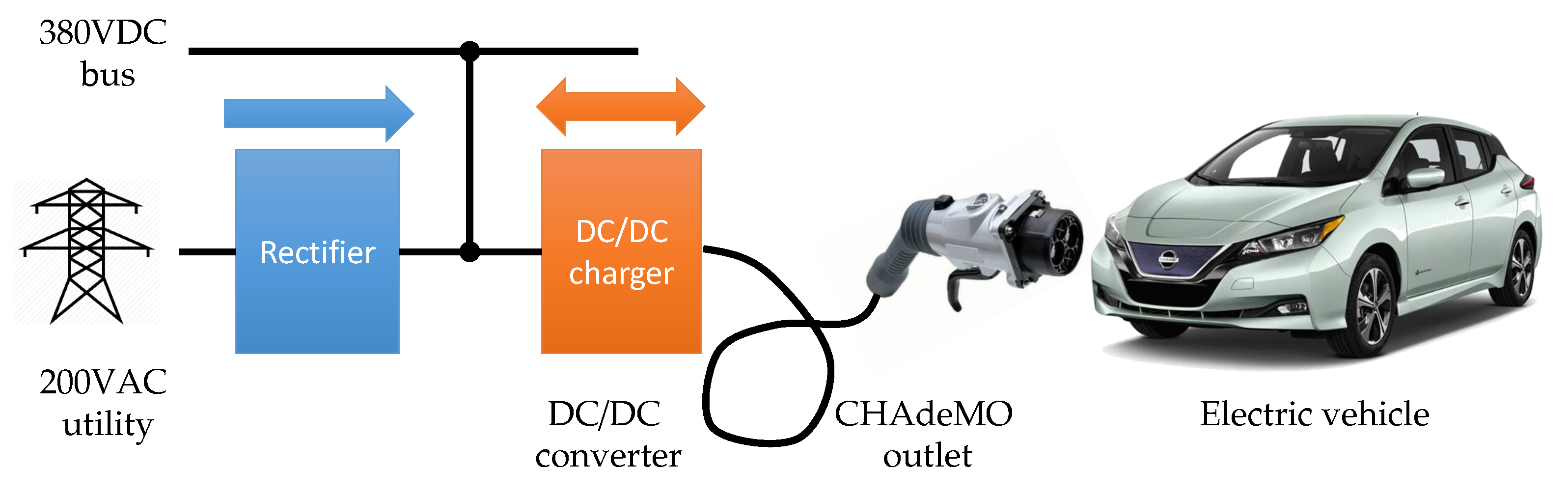
:1. Introduction
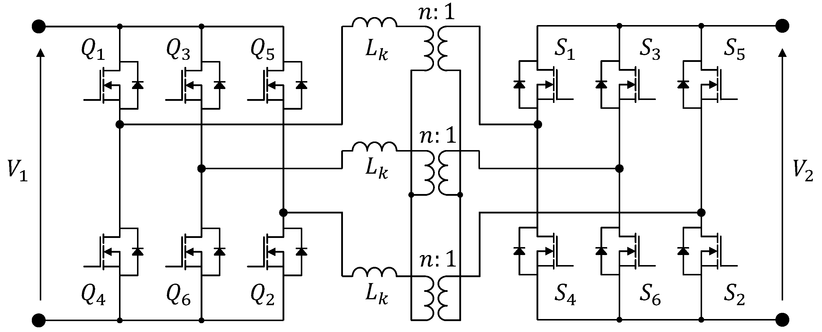
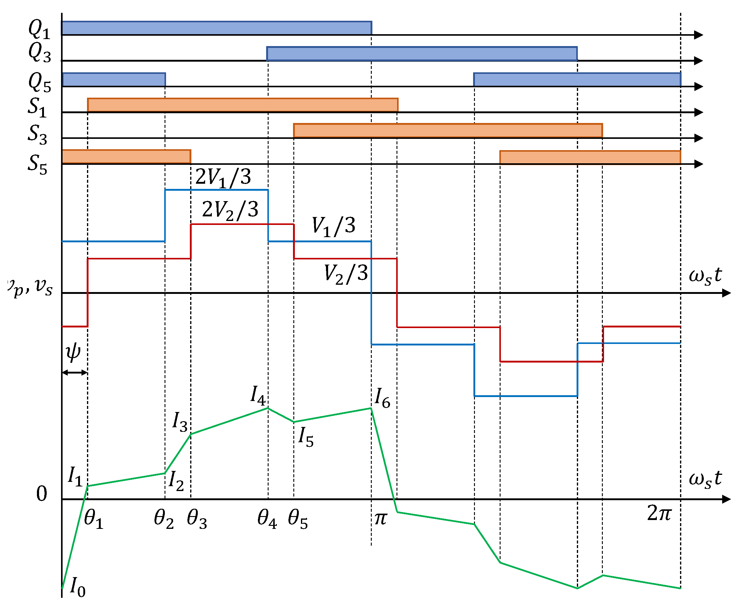
2. Steady State Analysis
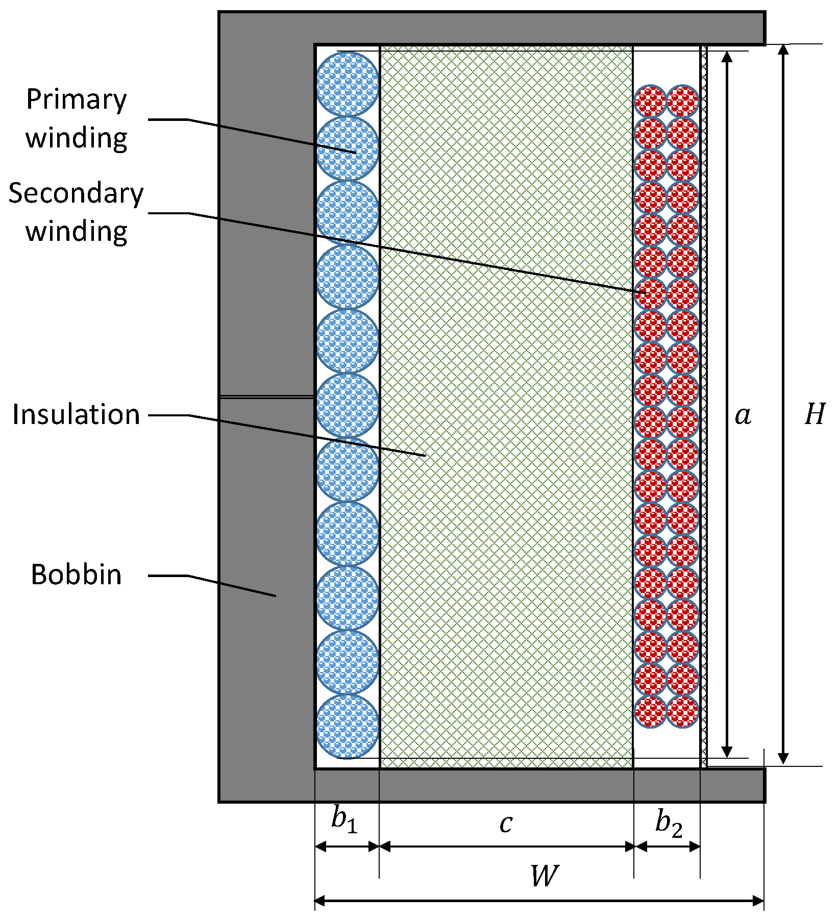
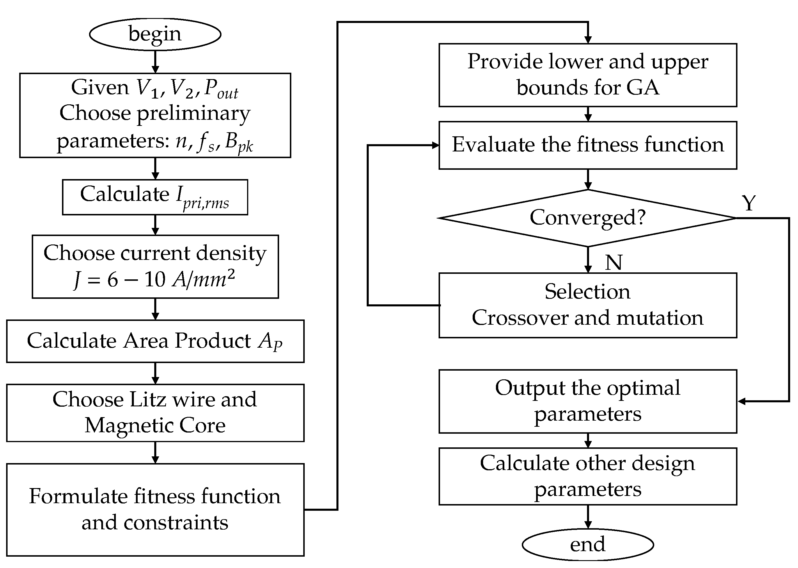
3. Transformer Design
- Maximum output power;
- Nominal input and output voltages;
- Current density (J = 6 − 10 A/mm);
- Window utilization factor ( = 0.2 − 0.4 for transformer);
- Initial switching frequency and flux density.
4. Power Loss Modeling
4.1. Power Electronics Loss
4.2. Transformer Loss
4.3. Capacitor Loss
5. Optimization
6. Results and Discussion
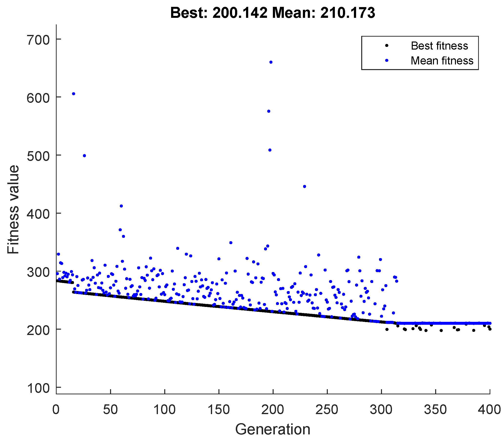
6.1. Optimization Results
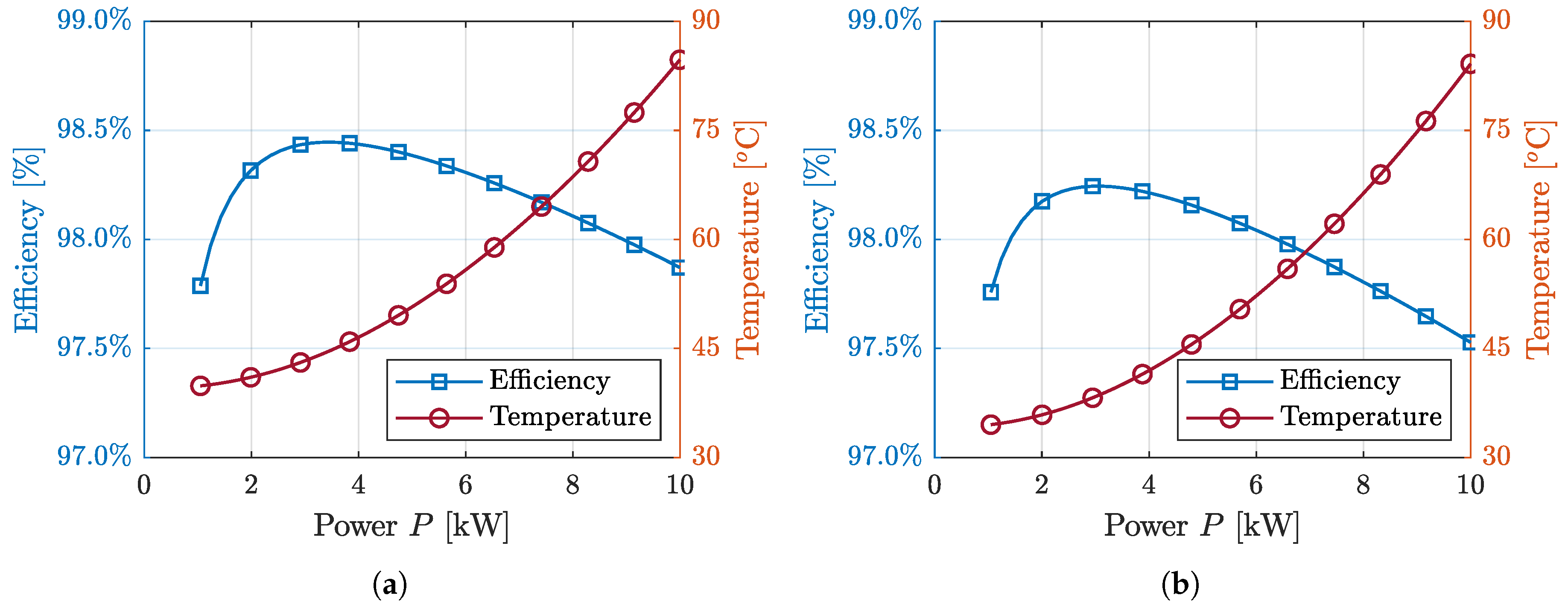
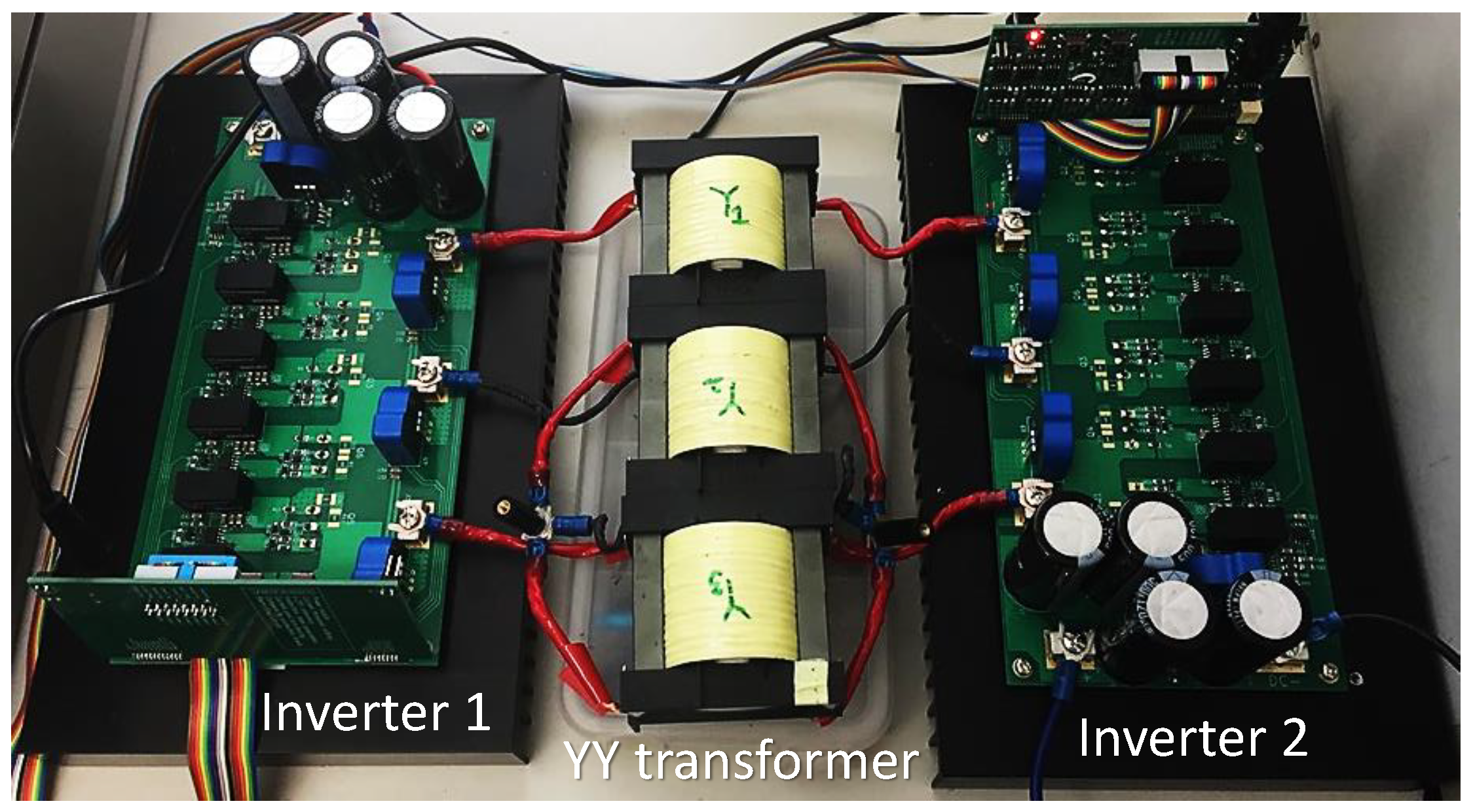
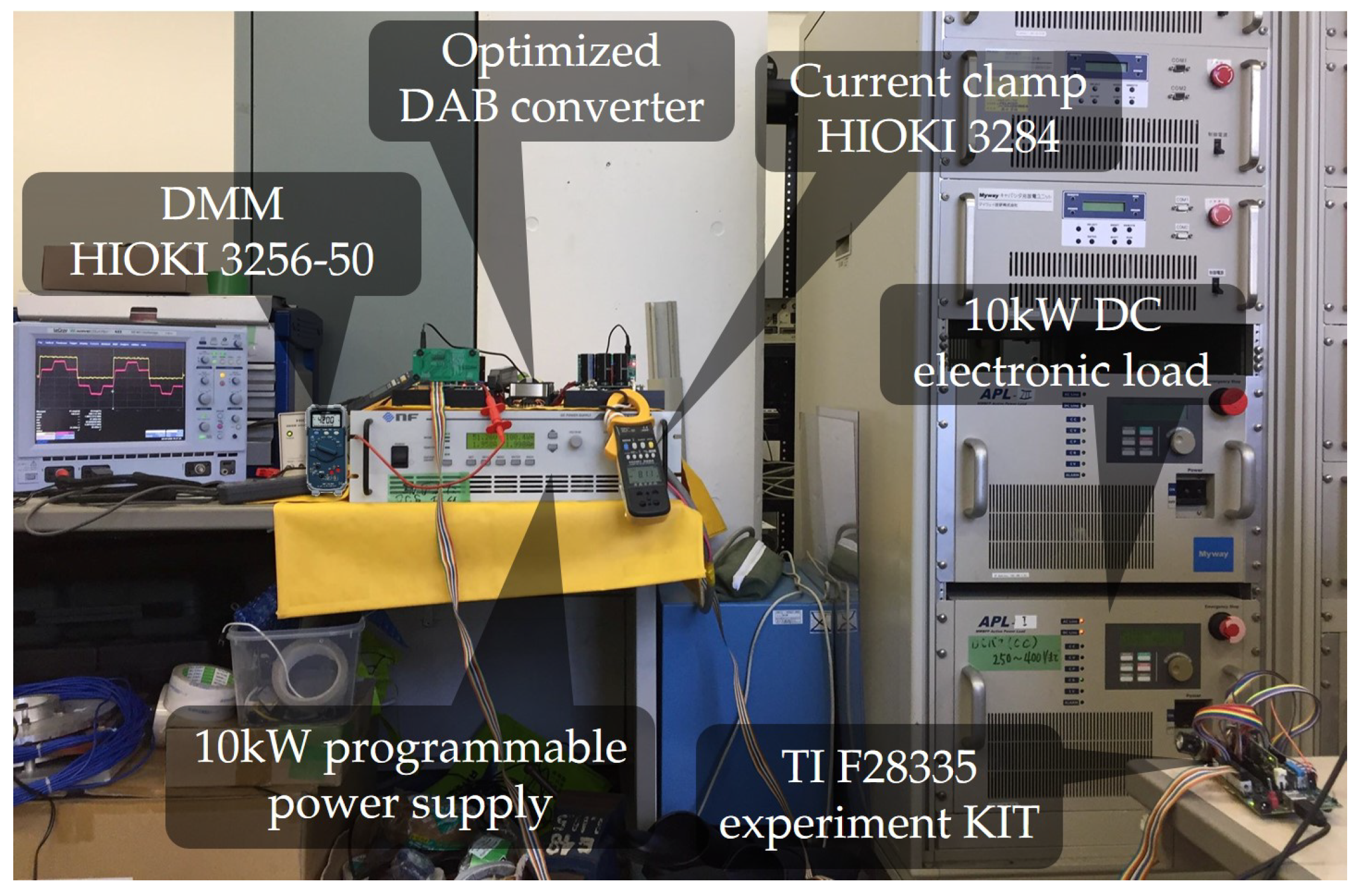
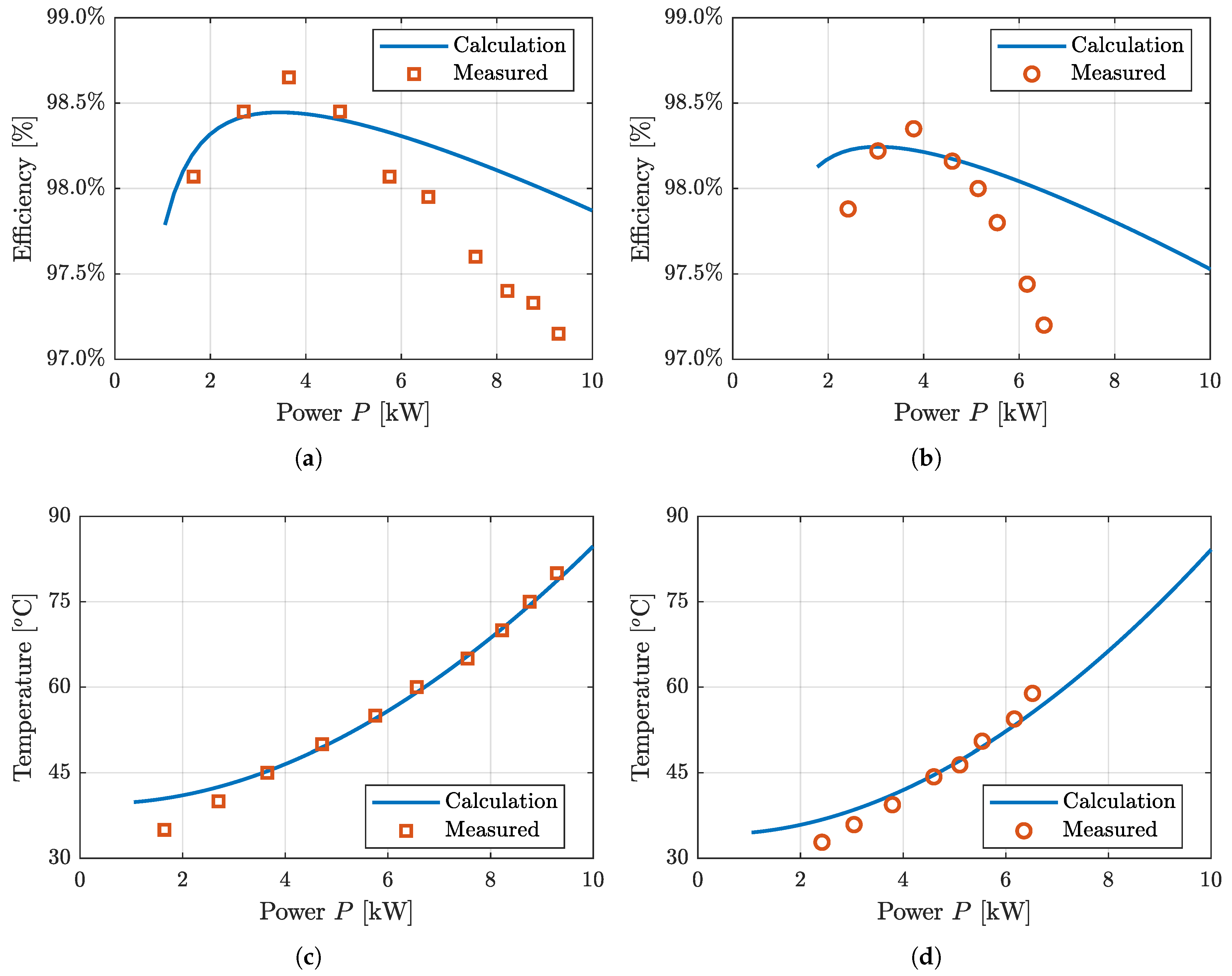
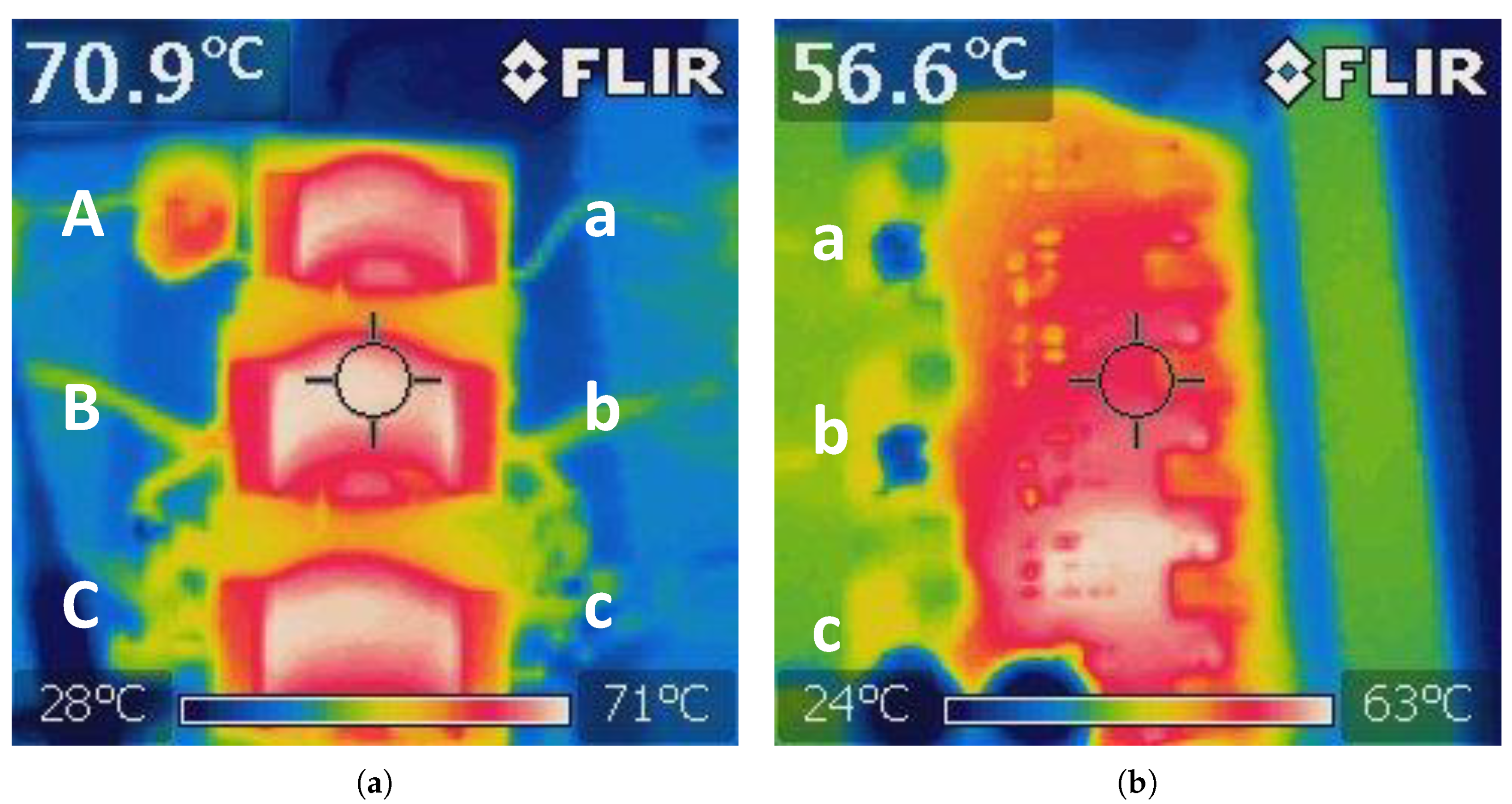
6.2. Simulation and Experimental Results
7. Conclusions
Author Contributions
Funding
Conflicts of Interest
References
- Kempton, W.; Tomić, J. Vehicle-to-grid power implementation: From stabilizing the grid to supporting large-scale renewable energy. J. Power Sources 2005, 144, 280–294. [Google Scholar] [CrossRef]
- Ota, Y.; Taniguchi, H.; Nakajima, T.; Liyanage, K.M.; Baba, J.; Yokoyama, A. Autonomous distributed V2G (vehicle-to-grid) satisfying scheduled charging. IEEE Trans. Smart Grid 2011, 3, 559–564. [Google Scholar] [CrossRef]
- Uddin, K.; Moore, A.D.; Barai, A.; Marco, J. The effects of high frequency current ripple on electric vehicle battery performance. Appl. Energy 2016, 178, 142–154. [Google Scholar] [CrossRef] [Green Version]
- He, P.; Khaligh, A. Comprehensive analyses and comparison of 1 kW isolated DC–DC converters for bidirectional EV charging systems. IEEE Trans. Transp. Electrif. 2016, 3, 147–156. [Google Scholar] [CrossRef]
- Zhu, L.; Taylor, A.R.; Liu, G.; Bai, K. A Multiple-Phase-Shift Control for a SiC-Based EV Charger to Optimize the Light-Load Efficiency, Current Stress, and Power Quality. IEEE J. Emerg. Sel. Top. Power Electron. 2018, 6, 2262–2272. [Google Scholar] [CrossRef]
- Haghbin, S.; Alatalo, M.; Yazdani, F.; Thiringer, T.; Karlsson, R. The design and construction of transformers for a 50 kW three-phase dual active bridge dc/dc converter. In Proceedings of the 2017 IEEE Vehicle Power and Propulsion Conference (VPPC), Belfort, France, 11–14 December 2017; pp. 1–5. [Google Scholar]
- van Hoek, H.; Neubert, M.; De Doncker, R.W. Enhanced modulation strategy for a three-phase dual active bridge—Boosting efficiency of an electric vehicle converter. IEEE Trans. Power Electron. 2013, 28, 5499–5507. [Google Scholar] [CrossRef]
- Baars, N.H.; Everts, J.; Wijnands, C.G.; Lomonova, E.A. Performance evaluation of a three-phase dual active bridge dc–dc converter with different transformer winding configurations. IEEE Trans. Power Electron. 2016, 31, 6814–6823. [Google Scholar] [CrossRef]
- Segaran, D.; Holmes, D.; McGrath, B. Comparative analysis of single-and three-phase dual active bridge bidirectional dc-dc converters. Aust. J. Electr. Electron. Eng. 2009, 6, 329–337. [Google Scholar] [CrossRef]
- Mainali, K.; Tripathi, A.; Madhusoodhanan, S.; Kadavelugu, A.; Patel, D.; Hazra, S.; Hatua, K.; Bhattacharya, S. A Transformerless Intelligent Power Substation: A three-phase SST enabled by a 15-kV SiC IGBT. IEEE Power Electron. Mag. 2015, 2, 31–43. [Google Scholar] [CrossRef]
- Iyer, V.M.; Gulur, S.; Bhattacharya, S. Optimal design methodology for dual active bridge converter under wide voltage variation. In Proceedings of the 2017 IEEE Transportation Electrification Conference and Expo (ITEC), Chicago, IL, USA, 22–24 June 2017; pp. 413–420. [Google Scholar]
- Wojda, R.; Kazimierczuk, M. Winding resistance of litz-wire and multi-strand inductors. IET Power Electron. 2012, 5, 257–268. [Google Scholar] [CrossRef]
- Qin, H.; Kimball, J.W.; Venayagamoorthy, G.K. Particle swarm optimization of high-frequency transformer. In Proceedings of the IECON 2010-36th Annual Conference on IEEE Industrial Electronics Society, Glendale, AZ, USA, 7–10 November 2010; pp. 2914–2919. [Google Scholar]
- Jauch, F.; Biela, J. Generalized modeling and optimization of a bidirectional dual active bridge DC-DC converter including frequency variation. IEEJ J. Ind. Appl. 2015, 4, 593–601. [Google Scholar] [CrossRef] [Green Version]
- Nguyen, D.D.; Kazuto, Y.; Katou, A.; Yoshida, S. Design optimization of a three-phase Dual-Active-Bridge converter for charging stations. In IEEE Vehicle Power and Propulsion Conference—VPPC 2019; IEEE: Hanoi, Vietnam, 2019; in process. [Google Scholar]
- McLyman, C.W.T. Transformer and Inductor Design Handbook; CRC Press: Boca Raton, FL, USA, 2016. [Google Scholar]
- Kachitvichyanukul, V. Comparison of three evolutionary algorithms: GA, PSO, and DE. Ind. Eng. Manag. Syst. 2012, 11, 215–223. [Google Scholar] [CrossRef] [Green Version]
- Global Optimization Toolbox. Available online: https://www.mathworks.com/products/global-optimization.html (accessed on 20 November 2019).
- Finite Element Method Magnetics 4.2. Available online: http://www.femm.info/wiki/HomePage (accessed on 20 November 2019).


| Parameter | Symbol | Value |
|---|---|---|
| Input voltage | 380 V | |
| Output voltage | 240−480 V | |
| Nominal output voltage | 380 V | |
| Rated power | P | 10 kW |
| Maximum temperature rise | 70 C | |
| Preliminary frequency | 50 kHz | |
| Preliminary phase shift | 30 degrees | |
| Preliminary peak flux density | 250 mT | |
| Calculated inductance | 15.56 H | |
| Desired current density | J | 9 A/mm |
| Selected wire | Litz 1050AWG44 | |
| Selected ferrite core | ETD54/28/19 (N87) | |
| SiC MOSFET | CREE C2M0040120D |
| Parameter | Symbol | Lower Bound | Upper Bound |
|---|---|---|---|
| Switching frequency | 50 kHz | 300 kHz | |
| Peak flux density | 50 mT | 250 mT | |
| Leakage inductance | 1 H | 10 H | |
| Voltage conversion ratio | M | 0.5 | 2 |
| Parameter | Symbol | Optimized Value | Modified Value | Competing Value | Unit |
|---|---|---|---|---|---|
| Switching frequency | 72.71 | 75 | 100 | kHz | |
| Peak flux density | 137.6 | 133.13 | 97.68 | mT | |
| Leakage inductance | 5.05 | 5.05 | 5.05 | H | |
| Conversion ratio | M | 1 | 1 | 1 | |
| Number of turns | : | 15:15 | 15:15 | 15:15 | |
| Phase shift angle | 13.1 | 13.54 | 18.46 | degrees | |
| AC resistance | 31.86 | 31.99 | 33.61 | m | |
| Transformer temperature rise | 70.0 | 69.75 | 69.15 | C | |
| Heatsink temperature rise | 40.7 | 41.44 | 49.73 | C | |
| Power electronics loss | 162.80 | 165.76 | 198.93 | W | |
| Transformer loss | 42.97 | 42.78 | 42.34 | W | |
| Total loss | 210.02 | 212.94 | 247.24 | W | |
| Efficiency@ | 97.9% | 97.87% | 97.53% |
| Parameter | Symbol | Calculation | FEA | Measurement | Unit | ||
|---|---|---|---|---|---|---|---|
| Leakage inductance | 5.05 | 4.87 | 4.92 | 4.9 | 4.82 | H | |
| Magnetizing inductance | 1.2 | 1.17 | 1.33 | 1.13 | 1.24 | mH | |
| AC resistance @ | 31.99 | 30.81 | 36.5 | 36.5 | 35.2 | m | |
| Peak flux density | 133.13 | 149.9 | - | - | - | mT | |
| Copper loss | 10.8057 | 10.19 | - | - | - | W | |
| Core loss | 3.4555 | 3.03 | - | - | - | W | |
© 2019 by the authors. Licensee MDPI, Basel, Switzerland. This article is an open access article distributed under the terms and conditions of the Creative Commons Attribution (CC BY) license (http://creativecommons.org/licenses/by/4.0/).
Share and Cite
Nguyen, D.-D.; Bui, N.-T.; Yukita, K. Design and Optimization of Three-Phase Dual-Active-Bridge Converters for Electric Vehicle Charging Stations. Energies 2020, 13, 150. https://doi.org/10.3390/en13010150
Nguyen D-D, Bui N-T, Yukita K. Design and Optimization of Three-Phase Dual-Active-Bridge Converters for Electric Vehicle Charging Stations. Energies. 2020; 13(1):150. https://doi.org/10.3390/en13010150
Chicago/Turabian StyleNguyen, Duy-Dinh, Ngoc-Tam Bui, and Kazuto Yukita. 2020. "Design and Optimization of Three-Phase Dual-Active-Bridge Converters for Electric Vehicle Charging Stations" Energies 13, no. 1: 150. https://doi.org/10.3390/en13010150