Abstract
Modular multilevel converters (MMCs) are expected to play an important role in future high voltage direct current (HVDC) grids. Moreover, advanced MMC topologies may include various submodule (SM) types. In this sense, the modeling of MMCs is paramount for HVDC grid studies. Detailed models of MMCs are cumbersome for electromagnetic transient (EMT) programs due to the high number of components and large simulation times. For this reason, simplified models that reduce the computation times while reproducing the dynamics of the MMCs are needed. However, up to now, the models already developed do not consider hybrid MMCs, which consist of different types of SMs. In this paper, a procedure to simulate MMCs having different SM topologies is proposed. First, the structure of hybrid MMCs and the modeling method is presented. Next, an enhanced procedure to compute the number of SMs to be inserted that takes into account the different behavior of full-bridge SMs (FB-SMs) and half-bridge submodules (HB-SMs) is proposed in order to improve the steady-state and dynamic response of hybrid MMCs. Finally, the MMC model and its control are validated by means of detailed PSCAD simulations for both steady-state and transients conditions (AC and DC faults).
1. Introduction
Multiterminal high voltage direct current (HVDC) grids are expected to be used to gather renewable energy from wind and solar power plants. At present, some multiterminal HVDC grids and several point-to-point HVDC links are already in operation to connect distant offshore wind farms to the onshore electrical grid [1,2,3]. For these grids, the modular multilevel converter (MMC) is the preferred topology because of its modularity, scalability, independent control of the active and reactive powers, capability to supply weak or passive networks, black-start capability, and ease to build multiterminal grids. Therefore, MMCs will be the backbone of future multiterminal HVDC grids [4].
To study the operation of the HVDC grids during steady-state and transient conditions, it is necessary to develop accurate MMC models. However, MMCs for HVDC grids have hundreds of levels, thus, thousands of submodules (SMs) and power semiconductor devices. This high number of semiconductor devices hinders the development of detailed models in electromagnetic transient (EMT) programs that include every single component owing to the computation burden and simulation times. For this reason, simplified models that accurately reproduce its dynamics are required [5].
Depending on the aim of the study, models with different levels of detail have been proposed in the literature [6,7]. Detailed IGBT-based models consider an in-depth representation of the power switches, including snubber circuits and the nonlinear behavior of the diodes and IGBTs. These models accurately replicate the nonlinear behavior of the switching events and allow the simulation of specific conditions such as blocked states, switching and conduction losses, converter start-up procedures, or internal converter faults. Hence, they are the most complex and accurate models but the computational burden for EMT programs makes their use for power system studies difficult. For these reasons, these models are usually implemented on FPGAs as in [8,9,10] and used as a reference for the validation of simplified models [6].
Simplified IGBT-based models use linear passive components (resistors, inductors, and capacitors) to represent the power semiconductor devices. A two-state resistor with a small value, , for the conduction state of the power devices and a large value, , for the blocked state is employed in [11]. In [12] the power semiconductor devices are replaced by RLC equivalent circuits which take into account the influence of the inductive and capacitive components at high frequencies. However, in both cases the vast number of nodes generates large admittance matrices (their size equals the number of nodes) that have to be inverted. Moreover, every time there is a switching operation, the admittance matrices change and must be reinverted, which leads to long simulation times. These large-scale admittance matrices are split up into several small-scale matrices to accelerate the simulation in [13]. To avoid the matrix inversions, a discrete modified nodal approach is proposed in [14], where the power devices are replaced by a small inductor for the ON state and a small capacitor for the OFF state. The inductance and capacitance values are selected in a way that the admittance matrices do not change regardless of the state of the power devices. Thus, the admittance matrices only have to be inverted once, which speeds up the simulation.
In the arm Thévenin equivalent models, each arm of the converter is modeled using a Thévenin or Norton equivalent circuit [11,15,16,17,18], which drastically reduces the number of nodes and improves the computational performance. The SMs are still considered individually, that is, there is a record of each SM state and capacitor voltage. However, given that the switching events are taken into account, small simulation steps are still required.
Simplified arm Thévenin equivalent models (continuous models or averaged value models (AVM)) also represent each arm by a Thévenin or Norton equivalent circuit. However, these models assume that all capacitors are charged/discharged simultaneously, so the SM capacitor voltages within each arm are perfectly balanced. In this way, there is no record of the behavior of each individual SM and the switching events are neglected, which allows increasing the simulation time step and to reduce the computation time [19,20,21,22]. AVM in the dq rotating frame and phasorial models have also been proposed in [23,24,25,26]. However, they neglect high frequency dynamics, therefore, transients like faults are not accurately modeled.
High-level models represent the whole MMC with a three-phase AC voltage source and a DC current source. These models neglect the internal dynamics of the MMC since they assume that the capacitor voltages are perfectly balanced and the circulating currents are null [5,27,28]. However, transients like AC and DC faults are not accurately modeled.
On the other hand, MMCs based on half-bridge submodules (HB-SMs) have been commercially used for the last decade due to its simpler structure and lower losses [27,29]. However, HB-SMs are not able to block DC faults, which may hinder the development of multiterminal HVDC grids unless reliable DC circuit breakers are developed. Thus, other SM topologies, such as full-bridge SM (FB-SM), clamp-double SM (CD-SM), or clamp-single SM (CSSM) have been proposed [30,31]. These topologies do have DC fault blocking capability at the expense of higher semiconductor power device counting and losses. Alternatively, hybrid MMCs combine different SM types within each arm to enhance their performance [32,33,34].
For power grid studies of multiterminal HVDC grids, it is important to capture the interaction between the MMCs and the DC and AC grids. For this reason, it is necessary to properly represent the behavior of the MMCs during steady-state and transient conditions like AC and DC faults or SM block states. However, it is not paramount to model other internal aspects like SMs faults, switching and conduction losses, etc. In this regard, simplified arm Thévenin equivalent models offer a good tradeoff between accuracy and computational burden. These type of models assume that the dynamics of all SMs are the same, thus, the capacitor voltages are equal for all SMs. However, this assumption is no longer valid for hybrid MMCs that include different topologies of SMs. Hence, it is necessary to take into account the characteristics of hybrid MMCs. Up to now, hybrid MMCs have been analyzed using detailed IGBT-based models with a low number of SMs per arm in order to not excessively slow down the simulation [33,34] or arm Thévenin equivalent models [35]. Therefore, an AVM is required, which is more suitable and efficient for power grid studies.
In this paper a simplified arm Thévenin equivalent model for a half bridge–full bridge hybrid MMC that takes into account the different behavior of HB-SMs and FB-SMs is developed. Moreover, an enhanced algorithm to determine the number of SMs that have to be inserted, which also takes into account the different voltages of HB-SMs and FB-SMs, is proposed in order to improved the steady-state and dynamic response of the hybrid MMCs.
2. MMC Description
Figure 1 shows the structure of the hybrid MMC considered in this paper. Each arm consists of an arrangement of HB-SMs and FB-SMs, N being the total number of SMs in each arm (). The proportion of HB-SMs and FB-SMs depends on the objectives of the hybrid MMC, for instance, DC fault blocking capability or overmodulation [36].
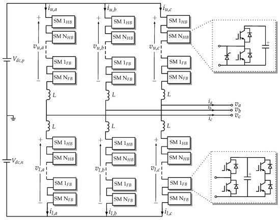
Figure 1.
Structure of the hybrid modular multilevel converter (MMC).
3. MMC Control
The overall control of the MMC is shown in Figure 2. The VSC control (outer control loops) regulates the AC active power/DC voltage and the reactive power in the dq frame, whereas the MMC control (inner control loops) regulates the SM capacitor voltages and the circulating current. The strategy for regulating the SM capacitor voltages is a two-fold scheme: (i) control of the arm energies and (ii) balancing the capacitor voltages.
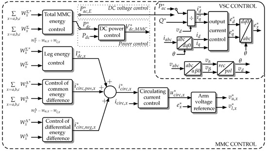
Figure 2.
Control of the MMC.
- Arm energy control
The arm energy control consists of the following four parts [37]:
- °
- Total converter energy control. This control regulates the total converter energy by setting the DC power if the MMC is in power control mode or the AC active power if the converter is in DC voltage mode.
- °
- Leg energy control. This control regulates the overall leg energy by means of the DC circulating current.
- °
- Common energy difference control. This control regulates the total energy difference between the upper and lower arms by using positive AC circulating currents.
- °
- Differential energy control. This control regulates the individual leg energy differences between the upper and lower arms by means of negative AC circulating currents.
The energy controls consist of proportional–integral (PI) controllers and feedforward terms that determine the DC and AC circulating currents, which, in turn, are regulated by means of proportional–integral–resonant (PIR) controllers.
From the VSC control and the MMC energy control, the arm voltage references are computed as follows:
where and are the positive and negative pole voltages, respectively, is the reference of output AC voltage for the phase x (), and is the reference for the internal voltage needed to control the circulating currents.
The insertion indexes are:
where and are the SM capacitor voltages of the upper and lower arms, respectively, of the phase x.
Considering the nearest level control (NLC), the number of SMs to be inserted is:
where the round function returns the nearest integer.
- Capacitor balancing control
The capacitor balancing algorithm (CBA) determines which SMs have to be inserted and bypassed at instant k to keep the SM capacitor voltages within each arm balanced, Figure 3.
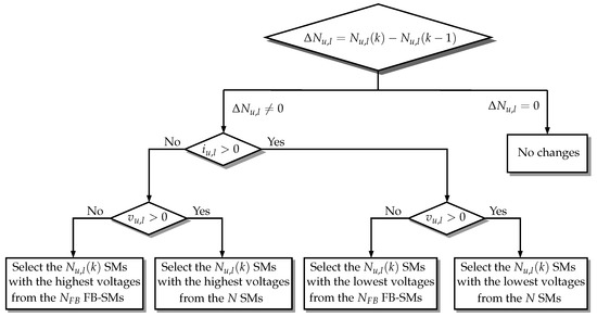
Figure 3.
Capacitor balancing algorithm.
3.1. Enhanced Control
If the MMC arms only have to insert positive arm voltages, both HB-SMs and FB-SMs can be used, and all SM capacitor voltages are virtually the same thanks to the CBA. However, if the MMC arms have to generate positive and negative voltages, only the FB-SMs can be employed for the negative voltages. Therefore, when the arm voltage is negative, the FB-SMs are charged/discharged, depending on the arm’s current direction, whereas the HB-SMs voltages remain constant. As a result, the capacitor voltages of the FB-SMs and HB-SMs are no longer the same. If the modulation indexes are calculated using Equation (2), the voltage inserted will be slightly different from that expected and the transient response of the MMC is worsened.
To overcome the aforementioned drawback, the use of the average capacitor voltages of those SMs that are going to be connected is proposed in this paper. However, which SMs will be inserted is unknown before calculating the modulating indexes and using the CBA. Nevertheless, taking into account that only a few SMs change their state every time there is a switching event, the average capacitor voltages of the SMs that are already connected is employed. In this way, the new insertion indexes are computed as follows:
where and are binary functions (0,1) that contain the state of the SMs of the upper and lower arms, respectively. and are the number of SMs connected in the upper and lower arms, respectively. With the proposed modulation indexes, only the SMs that are connected are used to compute the summation. Next, the obtained voltage is scaled up to get the modified total arm voltage as if all SMs had the same voltage as the inserted SMs. Once the new modulation indexes are computed, the number of SMs to be connected can be obtained using Equation (3).
4. Hybrid MMC Modeling
A simplified arm Thévenin equivalent model for hybrid MMCs is derived in this section with the aim of accurately reproducing the MMC behavior during both steady-state and transient conditions caused by AC or DC short-circuits. Moreover, it also considers the blocked state of the SMs. During normal operation, each arm is replaced by a voltage source and a resistor, regardless the number of SMs. Thus, the simulation time is not affected by the number of levels of the MMC.
4.1. SM Equivalent Circuit
The power semiconductor switches are modeled according to the simplified V-I curve shown in Figure 4, where the nonlinear behavior is neglected. The on-state is modeled by the forward voltage drop and a low-value resistor. The off-state is modeled with a resistor whose value is considered to be infinite. Taking into account the previous considerations, the SMs, irrespective of their type, are replaced by an equivalent resistor, , and an equivalent voltage source, , as shown in Figure 5.
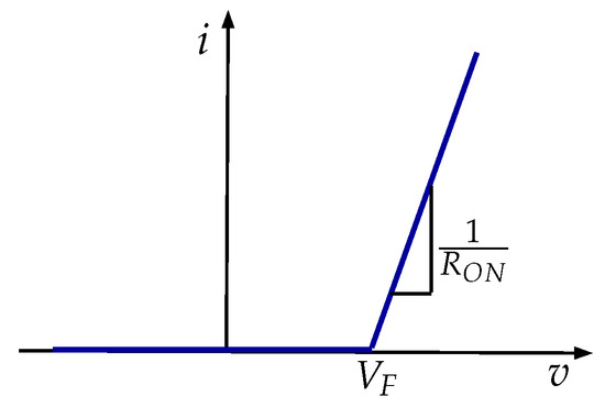
Figure 4.
V-I curve of the power semiconductor devices.
Figure 5.
Thévenin equivalent circuit of the submodules (SMs).
For HB-SMs, according to the current paths for the three possible states (bypassed, inserted, and blocked) shown in Figure 6, the values of the equivalent resistor () and voltage source () are presented in Table 1, where and are the conduction resistances of the IGBTs and the diodes, respectively, and are the forward voltages of the IGBTs and diodes, respectively, and is the capacitor voltage.
Figure 6.
States and current paths for half-bridge submodules (HB-SMs): (a) bypassed; (b) inserted; (c) blocked.

Table 1.
Values of the voltage source and the resistor for the HB-SM equivalent circuit.
For FB-SMs, according to the current paths for the three possible states (bypassed, inserted, and blocked) shown in Figure 7, Figure 8 and Figure 9, the values of the equivalent resistor () and voltage source () are presented in Table 2.
Figure 7.
Current path for the bypassed state of the full-bridge submodules (FB-SMs).
Figure 8.
Current path for the inserted state of the FB-SMs: (a) positive voltage; (b) negative voltage.
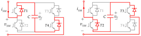
Figure 9.
Current path for the blocked state of the FB-SMs.
Table 2.
Values of the voltage source and the resistor for the FB-SM equivalent circuit.
4.2. Simplified Arm Thévenin Equivalent Model
For the normal operation of the MMC, the arm equivalent circuit is obtained from the number of inserted SMs calculated using Equations (3) and (4). The values of the equivalent voltage source and the resistor are computed as follows:
MMCs used in power systems have hundreds of SMs per arm, so the generated voltage waveform is virtually sinusoidal as shown in Figure 10. Hence, it can be assumed that the generated output voltage equals its reference. In this way the switching events resulting from inserting or bypassing SMs can be neglected and the simulation time step can be increased from few microseconds to several tens of microseconds, which drastically boosts the speed of the simulations. However, this simplification implies that: (i) there is no longer an individual record of the voltage of each SM, (ii) all SMs have the same capacitor voltage. Hence, the capacitor voltages are computed as follows:
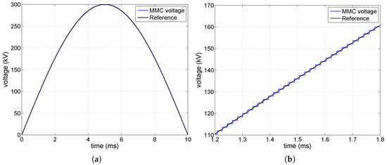
Figure 10.
Output MMC voltage and its reference. (a) MMC voltage and its reference; (b) zoom in of the MMC voltage and its reference.
For hybrid MMCs, it is necessary to take into account the different behavior of HB-SMs and FB-SMs if negative voltages are required. In this case, the insertion indexes of both types of SMs are different and the capacitor voltages of FB-SMs and HB-SMs can differ. The insertion indexes for the FB-SMs and HB-SMs are calculated according to the flow chart shown in Figure 11. For the sake of clarity, the subscripts related to the upper and lower arms are neglected. Hence, v is the arm voltage reference ( for the upper arm and for the lower arm) and i is the arm current ( for the upper arm and for the lower arm). Similarly, is the insertion index for the HB-SMs ( for the upper arm and for the lower arm) and is the insertion index for the FB-SMs ( for the upper arm and for the lower arm).
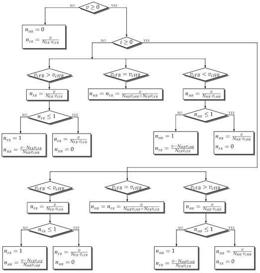
Figure 11.
Computation of the modulation indexes during normal operation of the MMC.
Figure 12 shows the arm Thévenin equivalent circuit. During normal operation the switches y are open whereas the switch is closed. Thus, the equivalent circuit consists of a variable voltage source and a resistor, regardless the number of SMs. The values of the arm voltage source, , and the arm resistor, for the arm Thévenin equivalent circuit are computed according to the flow chart shown in Figure 13.
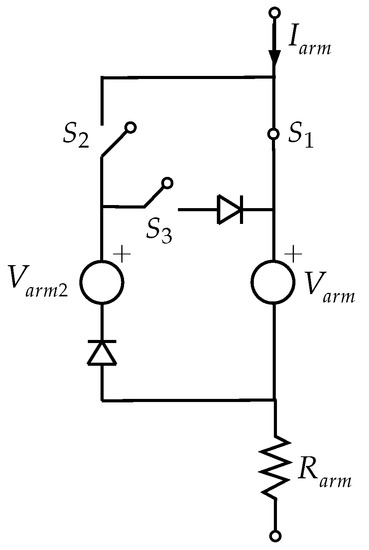
Figure 12.
Arm Thévenin equivalent circuit.
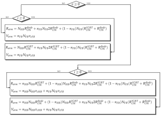
Figure 13.
Values of the arm equivalent Thévenin circuit.
Next, the capacitor voltages for the HB-SMs and FB-SMs are updated as follows:
The behavior of the MMC when it is blocked depends on the SM type and the arm current direction. For HB-SMs, if the arm current is positive, it flows through the diode of and charges the capacitor. On the other hand, if the arm current is negative, it flows through the diode of and the capacitor voltage remains constant, see Figure 6c. For FB-SMs, irrespective of the arm current direction, the current always flows through two diodes and charges the capacitor. Therefore, if the arm current is positive, it flows through the capacitor of all HB-SMs and all FB-SMs, which is equivalent to consider that all SMs are inserted. On the other hand, if the arm current is negative, it only flows through the capacitor of the FB-SMs, which is equivalent to consider that the FB-SMs are inserted and the HB-SMs are bypassed. Hence, the modulation indexes are computed as shown in Figure 14.
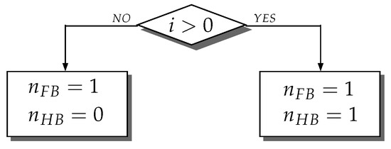
Figure 14.
Modulation indexes during the blocked state of the MMC.
To accurately model the MMC while it is blocked, the switches and are closed and the switch is opened, see Figure 12. In this way, the current flows through the voltage source when it is positive and through the voltage source when it is negative. The values of the voltage sources and the arm resistance are calculated as shown in Figure 15.
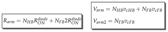
Figure 15.
Values of the arm equivalent Thévenin circuit for the blocked state of the MMC.
5. Results
In this section the proposed simplified arm Thévenin equivalent model is compared for its verification with the detailed (arm Thévenin equivalent) model developed by PSCAD [11,38]. Additionally, the enhanced control proposed in Section 3.1 is also validated. Figure 16 shows the electrical system used for the verification. The data of the MMC are presented in Table 3.
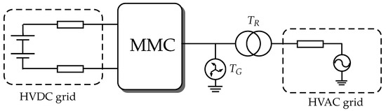
Figure 16.
Electrical system used for the verification of the simplified MMC model.
Table 3.
MMC data.
5.1. Control Validation
The MMC is connected to a symmetrical monopolar HVDC grid with a voltage of kV and controls the power exchanged between the DC and the AC grids. Provided that the DC voltage is lower than the AC voltage, FB-SMs are needed. Thus, the hybrid MMC has 300 HB-SMs and 100 FB-SMs per arm.
Initially the power reference is 0 and at s it is increased to 750 MW. The results obtained with the conventional and the proposed enhanced control are shown in Figure 17a,b. A zoom in of the plots is shown in Figure 18a,b. The MMC power is shown in the first graph. The second graph depicts the circulating current. The average capacitor voltages of all SMs (red trace), FB-SMs (black trace), and HB-SMs (blue trace) are plotted in the third graph. It can be noted that the dynamics of the capacitor voltages of the HB-SMs and FB-SMs are different, which makes difficult an accurate control of the MMC as explained below. The arm voltage reference and the insertion indexes are shown in the fourth and fifth graphs, respectively.
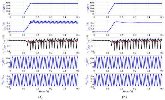
Figure 17.
Comparison between the conventional and proposed enhanced control. (a) Conventional control; (b) enhanced control.
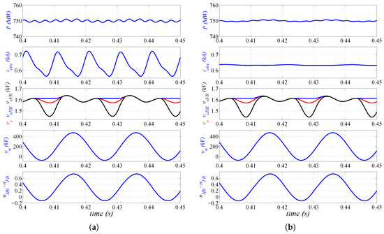
Figure 18.
Zoom in of the conventional and proposed enhanced controls. (a) Conventional control; (b) enhanced control.
The voltage that has to to inserted by the upper arm of phase a at s is kV as shown in the fourth graph of Figure 18a. From the third graph of Figure 18a, the average capacitor voltage is 1.58 kV. Thus, considering Equation (2a), the insertion index (fifth graph of Figure 18a) is:
The number of SMs to be inserted is obtained using Equation (3a):
However, given that the voltage to be inserted is negative, only FB-SMs can be used. This means that the inserted voltage is 47.68 kV (, 1.49 being the average capacitor voltage of the FB-SMs as shown in the third graph of Figure 18a), which differs from the reference voltage. As a result, the voltages generated by the MMC arms differ from their references, which creates some ripple in the output power (first graph of Figure 18a) and hinders the control of the circulating current (second graph of Figure 18a).
Given that the capacitor voltages of the HB-SMs and FB-SMs considerably differ since the HB-SMs have an average voltage of 1.61 kV and the average voltage of the FB-SMs is 1.49 kV, only the voltage of the SMs that are going to be inserted is used for computing the insertion index. The new insertion index and the number of SMs to be connected is:
Now, the inserted voltage is 50.66 kV (), which is closer to the reference voltage. As a result, the ripple of the output power and the AC components of the circulating current are reduced (first and second graphs of Figure 18b).
5.2. Verification of the Simplified Model
In this section the simplified arm Thévenin equivalent model for hybrid MMCs is verified for steady-state and transient conditions (AC and DC faults).
5.2.1. Normal Operation
The proposed model and the PSCAD model are compared for the normal operation of the MMC. As in the previous case, the MMC is connected to a symmetrical monopolar HVDC grid with a voltage of kV and controls the power exchanged between the DC and the AC grids. The hybrid MMC has 300 HB-SMs and 100 FB-SMs per arm.
Figure 19a,b shows the electrical variables of the AC and DC grids (active power, voltage, and current) for the detailed and simplified models, respectively, when the power is increased from 0 to 750 MW at s. The MMC controls the power exchanged with the AC grid (in this case, the power flows from the DC grid to the AC grid). Immediately, the MMC energy control reduces the DC voltage at the MMC terminals to increase the DC power imported from the DC in order to keep the SM capacitor voltages around their nominal value. It can be noticed that both models provide similar results during power changes.
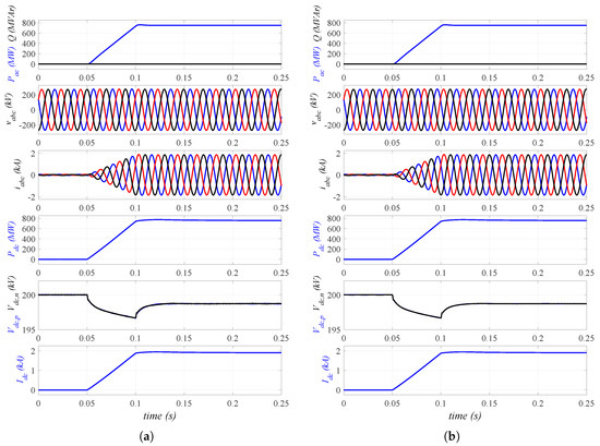
Figure 19.
External variables of the MMC during normal operation. (a) Detailed model; (b) simplified model.
Figure 20a,b shows the internal variables of the MMC (arm current and circulating current, average capacitor voltage, capacitor voltage of the HB-SMs, and capacitor voltage of the FB-SMs). The detailed model keeps a record of the state of each SM and each capacitor voltage. Therefore, the average capacitor voltages, along with the SMs with the highest and lowest capacitor voltages, are plotted in the third and fourth graphs of Figure 20a. Initially, the power exchanged with the AC grid is zero, thus, the arm currents are null and the capacitor voltages do not present any oscillation. When the power is changed, the arm currents increase accordingly and the capacitor voltages present the typical oscillation of the SM capacitors of MMCs. However, it can be seen that the CBA keeps the capacitor voltages perfectly balanced. Hence, it is acceptable to consider that all SMs have the same voltage as in the simplified model. In this way, it is not necessary to compute N capacitor voltages per arm, but only one, and the CBA can be neglected. Despite this simplification, the simplified model accurately reproduces the different behavior of the HB-SMs and FB-SMs, however, the computation burden is significantly reduced, which speeds up the simulation.
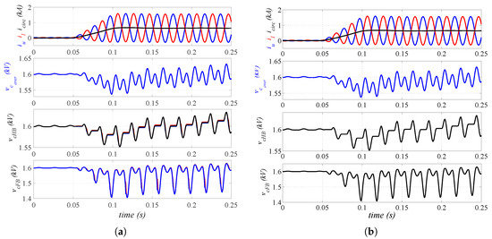
Figure 20.
Internal variables of the MMC during normal operation. (a) Detailed model; (b) simplified model.
Figure 21 and Figure 22 show the results for the reduced switching modulation strategy presented in [39]. Given that this modulation strategy reduces the switching frequency of the SMs, the variability among the SM capacitor voltages within an arm is higher as shown in the third and fourth graphs of Figure 22a. In this case, the differences between the average capacitor voltages provided by both models are slightly higher when compared with the previous CBA. However, the simplified model is still able to provide accurate results for both the external and internal variables of the MMC.

Figure 21.
External variables of the MMC during normal operation (reduced switching modulation). (a) Detailed model; (b) simplified model.
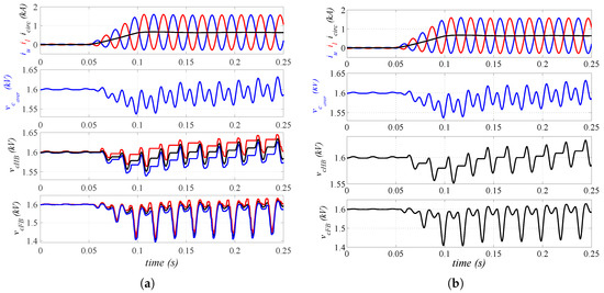
Figure 22.
Internal variables of the MMC during normal operation (reduced switching modulation). (a) Detailed model; (b) simplified model.
5.2.2. DC Faults
The response of the MMC, with 300 HB-SMs and 100 FB-SMs per arm, to a pole-to-ground DC fault is shown in Figure 23 and Figure 24. Figure 23 shows the external variables of the MMC, that is, the voltages and currents of the AC and DC sides. Figure 24 shows the internal variables of the MMC, that is, the arm currents and the HB-SM and FB-SM capacitor voltages of the upper and lower arms. Again, for the detailed model, the average capacitor voltages along with the maximum and minimum SM capacitor voltages are plotted. At s, the voltage of the positive pole drops to zero, the negative pole experiences an overvoltage, and the DC current increases rapidly. The SMs are blocked when an overcurrent of 1.5 pu is detected, plus 250 μs to take into account blocking delays. Altogether, the MMC is blocked about 2 ms after the fault onset. From that moment, the MMC behaves as a diode rectifier as can be seen in the AC current waveforms. Moreover, due to the counter voltage inserted by the FB-SMs, the fault current starts decreasing.
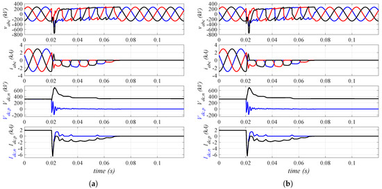
Figure 23.
Response of the MMC ( and ) to a DC fault when the MMC is blocked 2 ms after the fault onset. External variables. (a) Detailed model; (b) simplified model.
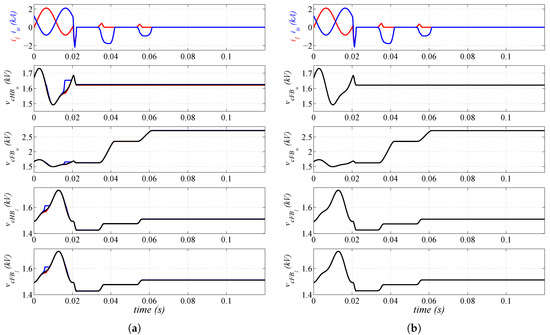
Figure 24.
Response of the MMC ( and ) to a DC fault when the MMC is blocked 2 ms after the fault onset. Internal variables. (a) Detailed model; (b) simplified model.
Once the MMC is blocked, the HB-SMs are bypassed so they behave like a rectifier. Therefore, their voltage remain constant as seen in the second graph of Figure 24. On the other hand, the FB-SMs insert a counter-voltage since the current flows through the capacitors. For this reason the FB-SMs are able to block the fault currents. However, given that only 100 FB-SMs are used in the simulation, the counter voltage is not high enough to block the DC fault. For this reason, the current keeps flowing through the capacitors until their voltage is high enough (see the third graph of Figure 24) to block the fault current shown in the second and fourth graphs of Figure 23. Obviously, this is not an acceptable situation due to the overvoltage in the capacitors of the FB-SMs. However, the aim of the simulation is to prove that both models offer similar results.
The same simulation is repeated for an MMC with 150 HB-SMs and 250 FB-SMs per arm. In the event of a DC fault, the FB-SMs insert a counter voltage that is higher than the peak value of the AC voltage. Therefore, in this case, the MMC is able to block the fault current as shown in the second and fourth graphs of Figure 25. As a result the current decays much faster to zero and the capacitor voltages remain almost constant (Figure 26). Thus, with an appropriate combination of HB-SMs and FB-SMs, the MMC is able to block the DC fault currents.
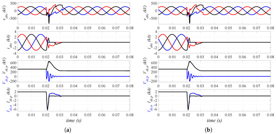
Figure 25.
Response of the MMC ( and ) to a DC fault when the MMC is blocked 2 ms after the fault onset. External variables. (a) Detailed model; (b) simplified model.
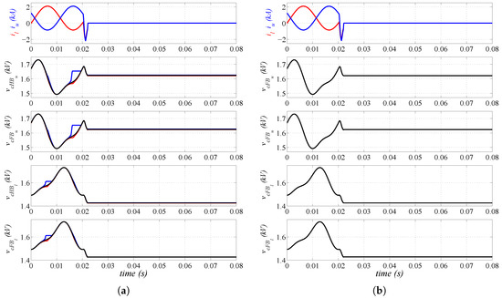
Figure 26.
Response of the MMC ( and ) to a DC fault when the MMC is blocked 2 ms after the fault onset. Internal variables. (a) Detailed model; (b) simplified model.
Figure 27 and Figure 28 present the results for a DC fault, but in this case the converter is blocked 25 ms after the fault onset to prove that the simplified model is also able to give accurate results while the MMC is not blocked. After an initial peak of the DC current due to the cable capacitance and SM capacitors, the DC fault current keeps increasing, which also causes SM capacitor overvoltages. Once the MMC is blocked, the current rapidly drops to zero due to the counter voltage inserted by the FB-SMs. This would not be an acceptable response due to the high overvoltage reached by the SM capacitors. However, the purpose of the simualtion is to prove that the simplified model is also valid in this situation. In all cases, it can be highlighted that the results obtained from the simplified model match with those of the detailed model.
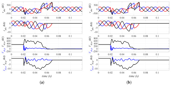
Figure 27.
Response of the MMC ( and ) to a DC fault when the MMC is blocked 25 ms after the fault onset. External variables. (a) Detailed model; (b) simplified model.
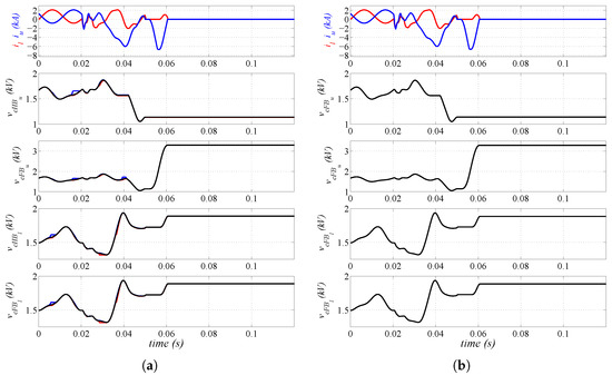
Figure 28.
Response of the MMC ( and ) to a DC fault when the MMC is blocked 25 ms after the fault onset. Internal variables. (a) Detailed model; (b) simplified model.
5.2.3. AC Faults
The response of the MMC, with 150 HB-SMs and 250 FB-SMs per arm, to an AC fault is shown in Figure 29 and Figure 30. Initially, the MMC transmits rated power (1200 MW) from the DC grid to the AC grid. At s there is a solid AC fault, so the AC voltage drops to zero (first graph of Figure 29). In response to the voltage drop, the AC currents increase to try to keep to power exchange (second and third graphs of Figure 29). However, these are limited by the current controllers to their nominal values, so no overcurrents are experienced. In this situation, it is not possible to exchange power with the AC grid (sixth graph of Figure 29), thus, in order to avoid overvoltages in the SM capacitors (second and thirds graphs of Figure 30), the SMs are blocked when a SM capacitor voltage of 1.25 is detected, which takes place around 15 ms after the fault onset. At this point, the AC and DC currents decay to zero (second and fifth graphs of Figure 29). Then, 50 ms after blocking the MMC, it is deblocked and connected to the AC grid. Once the AC voltage increases, the MMC injects reactive current (third graph of Figure 29) for voltage recovery according to the current-voltage profile shown in Figure 31, where the reactive current reference and the reactive current injected to the AC grid are plotted.
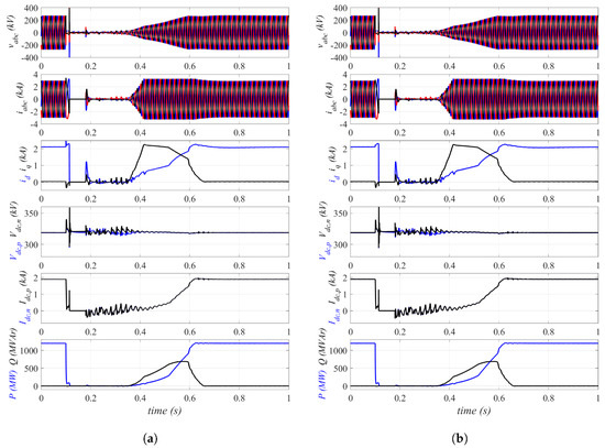
Figure 29.
Response of the MMC ( and ) to an AC fault. External variables. (a) Detailed model; (b) simplified model.
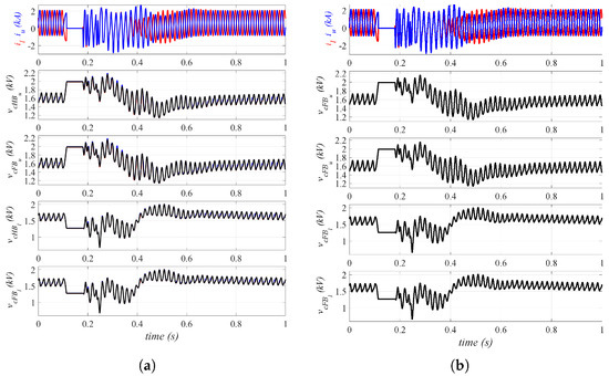
Figure 30.
Response of the MMC ( and ) to an AC fault. Internal variables. (a) Detailed model; (b) simplified model.
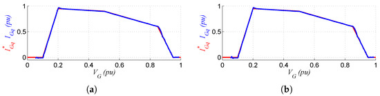
Figure 31.
Reactive current during the AC fault. (a) Detailed model; (b) simplified model.
Figure 30 shows the internal variables of the MMC, that is, the arm currents and the HB-SM and FB-SM capacitor voltages of the upper and lower arms. For the detailed model, the average capacitor voltages along with the maximum and minimum SM capacitor voltages are plotted.
Again, both the detailed and the simplified models offer similar results during the whole transient caused by the AC fault, even when the SMs are blocked and deblocked.
5.2.4. Simulation Efficiency
The simulations were made on a Microsoft Windows 7 platform with a 3 GHz Intel Core i5, 8 GB of RAM running PSCAD version 4.5. Table 4 tabulates the CPU times for both models for a three-second simulation. The solution time steps are 5 μs and 50 μs for the detailed and simplified models, respectively. It can be seen that the simplified model is about 50 times faster than the detailed model.
Table 4.
Simulation times.
5.2.5. Comparison with Other Models
The simplified model is compared in terms of accuracy and simulation times with other AVM models proposed in the literature. The SM capacitor voltage difference between the proposed simplified model and the detailed model are shown in Figure 32. The upper graphs show the error for the HB-SMs and the lower graphs show the error for the FB-SMs for the three cases studied previously, that is, normal operation, DC faults, and AC faults. During normal operation, the maximum error is 0.1%. This value increases to 0.22% and 0.3% during fast transients caused by DC and AC faults, respectively. Therefore, the errors are small and the model can be considered valid for its use in power systems simulation where the MMCs have a large number of SMs. A comparison with other models is shown in Table 5, where the errors of the proposed simplified model are slightly smaller than those presented for other models.
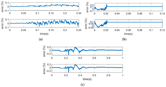
Figure 32.
SM capacitor voltage errors. Upper graphs: half-bridge submodules (HB-SMs). Lower graphs: FB-SMs. (a) Normal operation; (b) DC fault; (c) AC fault.
Table 5.
Error comparison.
Table 6 compares the simulation efficiency of the simplified model with other models proposed in the literature. It presents the ratio between the simulation time of an arm Thévenin equivalent model and the AVMs.
Table 6.
Simulation efficiency comparison.
6. Conclusions
In this paper, a simplified model of hybrid half-bridge full-bridge MMC intended for power grid studies of HVDC grids has been developed. The previously proposed AVM models in the literature for HB-MMCs assume that all SM capacitor voltages are well-balanced, therefore, their dynamics are the same. However, for hybrid MMCs that use half-bridge and full-bridge submodules, it is no longer valid since the dynamics of HB-SMs and FB-SMs are different when negative voltages have to be inserted. Thus, the simplifications carried out in previous works are no longer valid.
This paper presents a simplified model that allows an efficient and accurate simulation of MMCs. It assumes that the capacitor voltages are well-balanced, in this way, the switching events can be neglected and the simulation time can be considerably increased. However, it distinguishes the different behavior of HB-SMs and FB-SMs. Moreover, the outer and inner control of the MMC like the circulating current control are included in the model. Thus, the influence of different controls can be studied with the proposed model.
The proposed model has been compared with the model developed by PSCAD for several scenarios such as: power flow changes, DC faults, and AC faults. In all cases, the results obtained from both models are very close. However, the proposed simplified model lead to a 50-fold decrease in the simulation time.
Additionally, a modified procedure to compute the number of SMs to be inserted has been presented. Even if the SM capacitors voltages are perfectly balanced, the capacitor voltages of HB-SMs and FB-SMs can be different if negative voltages have to be inserted. Hence, this divergence in the HB-SMs and FB-SMs voltages is taken into account when the insertion indexes are computed in order to improve the response of the MMC.
Author Contributions
Conceptualization, R.V.-A.; methodology, R.V.-A. and J.F.; validation, R.V.-A. and J.F.; formal analysis, R.V.-A.; writing—original draft preparation, R.V.-A. All authors have read and agreed to the published version of the manuscript.
Funding
The present work was supported by the Spanish Ministry of Economy and EU FEDER Funds under grant DPI2017-84503-R. Project partially funded by the European Union through the Comunitat Valenciana 2014-2020 European Regional Development Fund (FEDER) Operating Program (grant IDIFEDER/2018/036).
Conflicts of Interest
The authors declare no conflict of interest.
Abbreviations
The following abbreviations are used in this manuscript:
| AC | Alternating current |
| DC | Direct current |
| HVDC | High voltage direct current |
| EMT | Electromagnetic transient |
| MMC | Modular multilevel converter |
| SM | Submodule |
| HB-SM | Half-bridge submodule |
| FB-SM | Full-bridge submodule |
| CBA | Capacitor balancing algorithm |
| AVM | Averaged value model |
| PI | Proportional-Integral |
| PIR | Proportional-Integral-Resonant |
| FPGA | Field-programmable gate array |
| IGBT | Insulated gate bipolar transistor |
References
- Tang, G.; He, Z.; Pang, H.; Huang, X.; Zhang, X.P. Basic topology and key devices of the five-terminal DC grid. CSEE J. Power Energy Syst. 2015, 1, 22–35. [Google Scholar] [CrossRef]
- Rao, H. Architecture of Nan’ao multi-terminal VSC-HVDC system and its multi-functional control. CSEE J. Power Energy Syst. 2015, 1, 9–18. [Google Scholar] [CrossRef]
- Michi, L.; Donnini, G.; Giordano, C.; Scavo, F.; Luciano, E.; Aluisio, B.; Vergine, C.; Pompili, M.; Lauria, S.; Calcara, L.; et al. New HVDC technology in Pan-European power system planning. In Proceedings of the 2019 AEIT HVDC International Conference (AEIT HVDC), Florence, Italy, 9–10 May 2019; pp. 1–6. [Google Scholar] [CrossRef]
- Gomis-Bellmunt, O.; Sau-Bassols, J.; Prieto-Araujo, E.; Cheah-Mane, M. Flexible converters for meshed HVDC grids: From Flexible AC transmission systems (FACTS) to Flexible DC grids. IEEE Trans. Power Deliv. 2019. [Google Scholar] [CrossRef]
- Saad, H.; Dennetiere, S.; Mahseredjian, J. On modelling of MMC in EMT-type program. In Proceedings of the 2016 IEEE 17th Workshop on Control and Modeling for Power Electronics (COMPEL), Trondheim, Norway, 27–30 June 2016; pp. 1–7. [Google Scholar] [CrossRef]
- Saad, H.; Dennetière, S.; Mahseredjian, J.; Delarue, P.; Guillaud, X.; Peralta, J.; Nguefeu, S. Modular Multilevel Converter Models for Electromagnetic Transients. IEEE Trans. Power Deliv. 2014, 29, 1481–1489. [Google Scholar] [CrossRef]
- Khan, S.; Tedeschi, E. Modeling of MMC for Fast and Accurate Simulation of Electromagnetic Transients: A Review. Energies 2017, 10, 1161. [Google Scholar] [CrossRef]
- Pang, H.; Zhang, F.; Bao, H.; Joos, G.; Wang, W.; Li, W.; Gregoire, L.A.; Zhai, X. Simulation of modular multilevel converter and DC grids on FPGA with sub-microsecond time-step. In Proceedings of the 2017 IEEE Energy Conversion Congress and Exposition (ECCE), Cincinnati, OH, USA, 1–5 October 2017; pp. 2673–2678. [Google Scholar] [CrossRef]
- Shen, Z.; Dinavahi, V. Real-Time Device-Level Transient Electrothermal Model for Modular Multilevel Converter on FPGA. IEEE Trans. Power Electron. 2016, 31, 6155–6168. [Google Scholar] [CrossRef]
- Tormo, D.; Idkhajine, L.; Monmasson, E.; Vidal-Albalate, R.; Blasco-Gimenez, R. Embedded real-time simulators for electromechanical and power electronic systems using system-on-chip devices. Math. Comput. Simul. 2019, 158, 326–343. [Google Scholar] [CrossRef]
- Gnanarathna, U.; Gole, A.; Jayasinghe, R. Efficient Modeling of Modular Multilevel HVDC Converters (MMC) on Electromagnetic Transient Simulation Programs. IEEE Trans. Power Deliv. 2011, 26, 316–324. [Google Scholar] [CrossRef]
- El-Khatib, W.Z.; Holbøll, J.; Rasmussen, T.W. High frequent modelling of a modular multilevel converter using passive components. In Proceedings of the International Conference on Power Systems Transients, Vancouver, BC, Canada, 18–20 June 2013. [Google Scholar]
- Xu, J.; Zhao, C.; Liu, W.; Guo, C. Accelerated Model of Modular Multilevel Converters in PSCAD/EMTDC. IEEE Trans. Power Deliv. 2013, 28, 129–136. [Google Scholar] [CrossRef]
- Zhang, F.; Yang, X.; Wang, K.; Xu, G.; Huang, L.; Chen, W. A discrete time-domain model for fast simulation of MMC circuits. In Proceedings of the 2016 IEEE 8th International Power Electronics and Motion Control Conference (IPEMC-ECCE Asia), Hefei, China, 22–26 May 2016; pp. 2366–2370. [Google Scholar] [CrossRef]
- Vidal-Albalate, R.; Belenguer, E.; Beltran, H.; Blasco-Gimenez, R. Efficient model for modular multi-level converter simulation. Math. Comput. Simul. 2016, 130, 167–180. [Google Scholar] [CrossRef]
- Ajaei, F.B.; Iravani, R. Enhanced Equivalent Model of the Modular Multilevel Converter. IEEE Trans. Power Deliv. 2015, 30, 666–673. [Google Scholar] [CrossRef]
- Xu, J.; Ding, H.; Fan, S.; Gole, A.M.; Zhao, C. Enhanced high-speed electromagnetic transient simulation of MMC-MTdc grid. Int. J. Electr. Power Energy Syst. 2016, 83, 7–14. [Google Scholar] [CrossRef]
- Ahmed, N.; Angquist, L.; Mahmood, S.; Antonopoulos, A.; Harnefors, L.; Norrga, S.; Nee, H.P. Efficient Modeling of an MMC-Based Multiterminal DC System Employing Hybrid HVDC Breakers. IEEE Trans. Power Deliv. 2015, 30, 1792–1801. [Google Scholar] [CrossRef]
- Ahmed, N.; Angquist, L.; Norrga, S.; Nee, H.P. Validation of the continuous model of the modular multilevel converter with blocking/deblocking capability. In Proceedings of the 10th IET International Conference on AC and DC Power Transmission (ACDC 2012), Birmingham, UK, 4–5 December 2012. [Google Scholar] [CrossRef]
- Ahmed, N.; Angquist, L.; Norrga, S.; Antonopoulos, A.; Harnefors, L.; Nee, H.P. A Computationally Efficient Continuous Model for the Modular Multilevel Converter. IEEE J. Emerg. Sel. Topics Power Electron. 2014, 2, 1139–1148. [Google Scholar] [CrossRef]
- Zhang, H.; Jovcic, D.; Lin, W.; Far, A.J. Average value MMC model with accurate blocked state and cell charging/discharging dynamics. In Proceedings of the 2016 4th International Symposium on Environmental Friendly Energies and Applications (EFEA), Belgrade, Serbia, 14–16 September 2016; pp. 1–6. [Google Scholar] [CrossRef]
- Yang, H.; Dong, Y.; Li, W.; He, X. Average-Value Model of Modular Multilevel Converters Considering Capacitor Voltage Ripple. IEEE Trans. Power Deliv. 2017, 32, 723–732. [Google Scholar] [CrossRef]
- Najmi, V.; Nazir, M.N.; Burgos, R. A new modeling approach for Modular Multilevel Converter (MMC) in D-Q frame. In Proceedings of the 2015 IEEE Applied Power Electronics Conference and Exposition (APEC), Charlotte, NC, USA, 15–19 March 2015; pp. 2710–2717. [Google Scholar] [CrossRef]
- Sinha, Y.; Nampally, A. Averaged model of modular multilevel converter in rotating DQ frame. In Proceedings of the 2016 IEEE International Conference on Renewable Energy Research and Applications (ICRERA), Birmingham, UK, 20–23 November 2016; pp. 319–324. [Google Scholar] [CrossRef]
- Jamshidi Far, A.; Jovcic, D. Small-Signal Dynamic DQ Model of Modular Multilevel Converter for System Studies. IEEE Trans. Power Deliv. 2016, 31, 191–199. [Google Scholar] [CrossRef]
- Wang, Q.; Ye, H.; Zhang, G. Improved dynamic phasor-based modeling and simulation of modular multilevel converter. In Proceedings of the 2017 IEEE Conference on Energy Internet and Energy System Integration (EI2), Beijing, China, 26–28 November 2017; pp. 1–6. [Google Scholar] [CrossRef]
- Peralta, J.; Saad, H.; Dennetiere, S.; Mahseredjian, J.; Nguefeu, S. Detailed and Averaged Models for a 401-Level MMC-HVDC System. IEEE Trans. Power Deliv. 2012, 27, 1501–1508. [Google Scholar] [CrossRef]
- Longze, K.; Lin, Z.; Fangyuan, L. Electromechanical modelling of modular multilevel converter based HVDC system and its application. In Proceedings of the 2017 IEEE Conference on Energy Internet and Energy System Integration (EI2), Beijing, China, 26–28 November 2017; pp. 1–6. [Google Scholar] [CrossRef]
- Coronado, L.; Longas, C.; Rivas, R.; Sanz, S.; Bola, J.; Junco, P.; Perez, G. INELFE: Main description and operational experience over three years in service. In Proceedings of the 2019 AEIT HVDC International Conference (AEIT HVDC), Florence, Italy, 9–10 May 2019; pp. 1–6. [Google Scholar]
- Marquardt, R. Modular Multilevel Converter: An universal concept for HVDC-Networks and extended DC-Bus-applications. In Proceedings of the International Power Electronics Conference (IPEC), Sapporo, Japan, 21–24 June 2010; pp. 502–507. [Google Scholar] [CrossRef]
- Xu, J.; Zhao, P.; Zhao, C. Reliability Analysis and Redundancy Configuration of MMC With Hybrid Submodule Topologies. IEEE Trans. Power Electron. 2016, 31, 2720–2729. [Google Scholar] [CrossRef]
- Zeng, R.; Xu, L.; Yao, L. An improved modular multilevel converter with DC fault blocking capability. In Proceedings of the 2014 IEEE PES General Meeting|Conference & Exposition, National Harbor, MD, USA, 27–31 July 2014; pp. 1–5. [Google Scholar] [CrossRef]
- Qin, J.; Saeedifard, M.; Rockhill, A.; Zhou, R. Hybrid Design of Modular Multilevel Converters for HVDC Systems Based on Various Submodule Circuits. IEEE Trans. Power Deliv. 2015, 30, 385–394. [Google Scholar] [CrossRef]
- Li, R.; Adam, G.P.; Holliday, D.; Fletcher, J.E.; Williams, B.W. Hybrid Cascaded Modular Multilevel Converter with DC Fault Ride-Through Capability for the HVDC Transmission System. IEEE Trans. Power Deliv. 2015, 30, 1853–1862. [Google Scholar] [CrossRef]
- Li, R.; Xu, L.; Guo, D. Accelerated switching function model of hybrid MMCs for HVDC system simulation. IET Power Electron. 2017, 10, 2199–2207. [Google Scholar] [CrossRef]
- Lin, W.; Jovcic, D.; Nguefeu, S.; Saad, H. Full-Bridge MMC Converter Optimal Design to HVDC Operational Requirements. IEEE Trans. Power Deliv. 2016, 31, 1342–1350. [Google Scholar] [CrossRef]
- Cui, S.; Sul, S.K. A Comprehensive DC Short-Circuit Fault Ride Through Strategy of Hybrid Modular Multilevel Converters (MMCs) for Overhead Line Transmission. IEEE Trans. Power Electron. 2016, 31, 7780–7796. [Google Scholar] [CrossRef]
- PSCAD. Available online: https://hvdc.ca/knowledge-base/topic:45/v: (accessed on 25 October 2019).
- Tu, Q.; Xu, Z.; Xu, L. Reduced Switching-Frequency Modulation and Circulating Current Suppression for Modular Multilevel Converters. IEEE Trans. Power Deliv. 2011, 26, 2009–2017. [Google Scholar] [CrossRef]


© 2020 by the authors. Licensee MDPI, Basel, Switzerland. This article is an open access article distributed under the terms and conditions of the Creative Commons Attribution (CC BY) license (http://creativecommons.org/licenses/by/4.0/).