1. Introduction
The multilevel topology of the converter is favorable for high-voltage circuits due to the reduction of voltage stress on switches. Aside from typical multilevel converters, such as the flying capacitor, neutral point clamped, and cascade bridges, various concepts of switched capacitor-based converters have been proposed recently. The switched capacitor (SC) technique is suitable for high-voltage gain converters and can be effectively used in power converters, which was proven in [
1,
2]. On the basis of the SC technique, such multilevel topologies include MRSCC (multilevel mesonant switched capacitor converter) [
3,
4,
5], modular capacitor clamped [
6,
7], resonant Ladder [
8], MMCCC (multilevel modular capacitor clamped converter), 6X [
9], converter with coupled inductors in various levels [
10], and converters presented in [
11,
12,
13,
14,
15,
16], where the topologies include a similar concept to MRSCC.
Another important quality of a power electronic converter is its bidirectional operation capability. It is required in a vast range of applications, which incorporates battery management. The analyzed MRSCC is made up of a basic SC structure, which makes it possible to transfer energy in both directions, similar to the converters presented in [
3,
4,
5,
13,
14,
15,
16,
17].
The four-level MRSCC converter analyzed in this study (
Figure 1a) is a very favorable solution when compared to well-established topologies. It comprises features of a bidirectional and multilevel topology. In MRSCC, voltage stress on the switches is equal to the voltage of a single cell; therefore, the benefit of switch voltage stress reduction is achieved. In comparison to the other concepts of SC converters, such as SCVMs (switched capacitor voltage multipliers) presented in [
18,
19], MRSCC is a multilevel concept that can be more favorable for high-voltage applications. Voltage stresses on some switches of SCVMs can reach the output voltage (the highest value). Due to the high voltage gain, low stress on switches, and bidirectional conversion ability, MRSCC can be a beneficial solution for the interconnection between DC voltage systems. Depending on applications, numerous DC voltage systems are often used nowadays [
20], and the required DC voltage reaches 1500 V [
17]. The microgrid connection is another prospective application of such a converter as well. Furthermore, in MRSCC, the energy is transferred via capacitors, which makes it possible to reduce the weight of the converter in comparison to solutions based on inductive components. In some applications, a low weight can be an important feature due to the requirements related to the assembling system components.
The basic concepts of three-level and four-level MRSCCs are presented in [
3], in which a detailed analysis of losses and selection of inductance can be found. In [
4], the four-level SC converter with loads connected asymmetrically was analyzed. In [
5], the first harmonic approximation analysis and basic experimental results of four-level 1.2 kV MRSCC based on SiC are presented. In [
13], as well as [
14], the basic structure of a multilevel SC converter is used in cascaded systems. However, the problems of topology modification and efficiency improvement in ZVS conditions were not investigated.
Recently, a lot of research has focused on the elimination or limitation of
Coss losses in different types of converters. However, very few of them present a solution for switched capacitor converters and especially multilevel ones. In [
15,
17], the
Coss losses were identified as an important factor in the power efficiency limitation of the voltage doubler based on the MRSCC concept. The solution for
Coss elimination is reported in [
15] for a MOSFET converter as well as in [
16] for GaN and in [
17] for SiC. Therefore, the methods for achieving ZVS (zero-voltage switching) in such a converter are demonstrated in those papers, but all of them are similar and limited to two-level (voltage doubler) MRSCC. The methods rely on the application of the special control pattern to switches in higher and lower voltage levels, for additional energy delivery to the resonant inductor before dead time intervals. The energy stored in the resonant inductor is then utilized for the
Coss voltage transition in dead time intervals. As reported in [
16], this technique is problematic in light load operations, due to significant switching frequency increases. Special control with cycle skipping is required for light load operation, which itself brings some power loss and is problematic due to parasitic oscillations [
21]. To mitigate this challenge, the authors in [
16,
17,
21] proposed to move the resonant inductor to the DC side of the converter. It eliminates most disadvantages; however, it still cannot be applied to converters with a number of levels higher than 2, since in higher levels of the converter, the resonant operation could not be achieved. In this paper, the solution with an additional small inductor further referenced as the commutation supporting inductor (
LSC) and small (commutation) capacitors connected across resonant branches is presented. This solution is free from the abovementioned limitations. It operates well at any load level, including an idle state, and can be applied for a converter with any number of voltage levels; however, it requires additional components.
Coss losses have an important impact on the efficiency of a high-frequency converter. A model of this type of loss in an SiC-based converter is analyzed in detail in [
22]. In the case of SC converters, which contain large numbers of switches, such as SCVM [
18,
19], and do not operate in ZVS mode,
Coss losses can become significant. The method for ZVS operation in SC converters with resonant inductors is an important research subject. It can be introduced to other SC topologies than MRSCC and the results of ZVS operation in an SiC-based converter presented in this paper can have even more general importance. In [
23,
24,
25,
26,
27,
28], SC converters with ZVS operation are presented. The presented approach for the ZVS problem solution is similar there and the converters use resonant inductors, which makes it possible to apply a phase shift switching or an operation above the resonant frequency for a charge reduction of the switch before it is turned on. The
Coss voltage transition method and ZVS operation is accomplished in this paper for four-level MRSCC and can be extended to a higher number of voltage levels, which is the main difference from previously presented solutions. Therefore, this paper confirms the merit of the MRSCC topology with introduced improvements. Furthermore, numerous new experimental results of Si and SiC MOSFETs based on bidirectional four-level MRSCC, such as the efficiency, voltage ratio measurements, and resonant circuit operation, are presented and compared in this paper. In essence, the main goal of this paper was to verify the concept of the topology modification towards efficiency improvement of four-level SiC-based and Si-based MRSCC converters with the major contributions of this paper being as follows:
A presentation of a modification of the MRSCC topology to achieve ZVS with no restrictions in terms of the number of voltage levels. A significant increase of the efficiency and significant decrease of idle power losses are achieved in comparison to the base topology by (almost) elimination of the Coss losses.
A comparison the SiC-based and Si-based MRSCC performance based on experimental results. It is demonstrated that the proposed method makes it possible to achieve a performance of the Si MOSFET design close to the outstanding SiC-based one.
The demonstration of MRSCC operation in a boost mode as well as in buck mode. It is accomplished in a test setup with two cascaded converters with a common high-voltage DC link (2 kV in the tested case). However, the load and the output voltage sensors operate on a low voltage (<1 kV), which is appropriate for precise voltage registration and efficiency measurement, and MRSCC is a bi-directional converter and such concept of a test setup configuration is justified. A similar approach can be found in [
15], which presents the regenerative test setup, composed of two resonant SC converters for efficiency. A single DC-DC converter with a high voltage ratio can be used in photovoltaic systems [
17] with a common DC link or DC grid on the output. The application of such converters as an interconnector between DC grids is their prospective application as well, especially as SiC-based solutions.
The paper is organized as follows. In
Section 2, the basics of operation of the MRSCC and simulation results are presented. In
Section 3, the problem of
Coss loss is addressed and a modification of base topology is proposed.
Section 4 includes a description of the back-to-back experimental setup and experimental results of MRSCC operation.
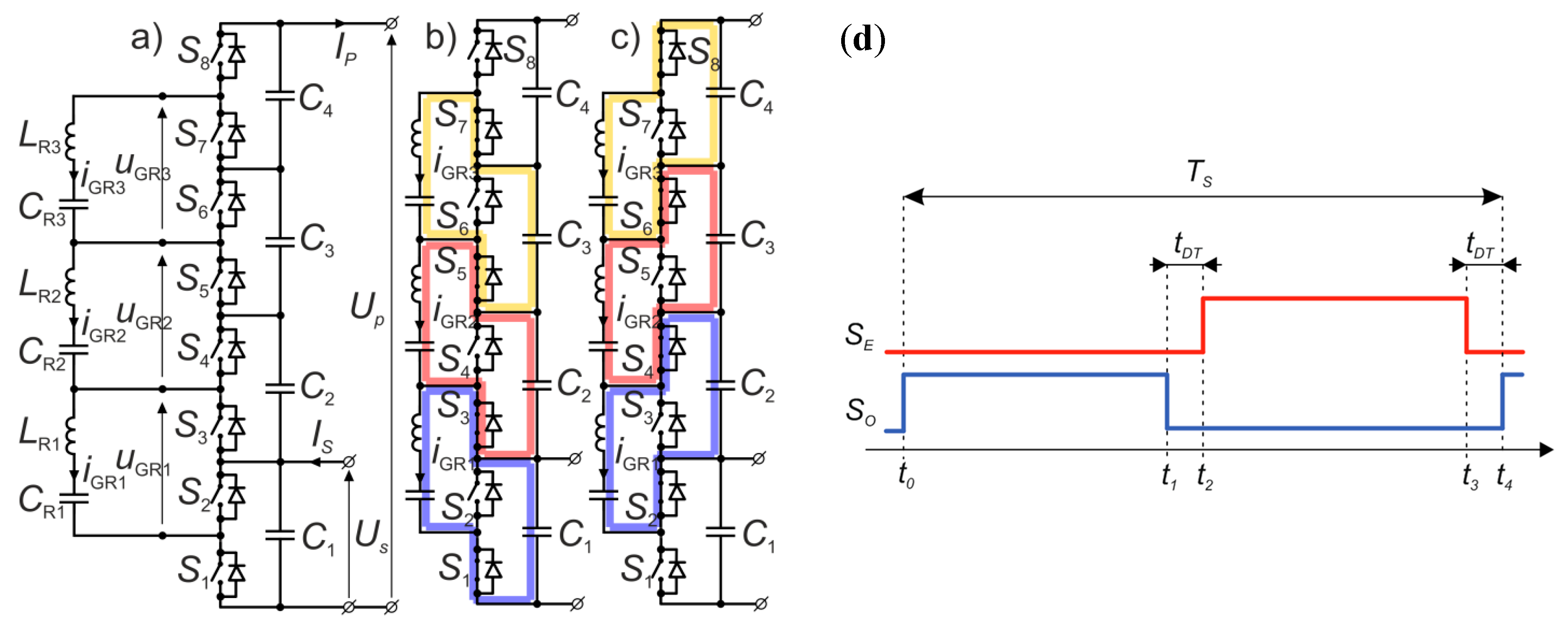
2. Principle of Operation of the Multilevel Resonant Switched Capacitor Converter (MRSCC)
Figure 1 presents the topology of the MRSCC. The principle of operation assumes charging and discharging of switched capacitors (
CR) in resonant circuits and energy exchange between DC capacitors
C1–
C4. Each voltage level contains two transistors in HB (half bridge) configuration, with appropriate driving circuits. All the resonant branches
CR1LR1-
CR3LR3 are tuned to the same resonant frequency. The control of the converter, in the general concept, requires alternating the switching of odd and even switches with a 50% duty ratio with the resonant frequency of the branches
CR1LR1-
CR3LR3. As a result, each resonant branch (
CRkLRk) is switched between two adjacent voltage level capacitors
Ck and
C(k+1) (
Figure 1b,c). The control signals are presented in
Figure 1d.
Voltages of the capacitors
C1-
C4 of MRSCC are nearly equalized. As a result, the voltage gain of the idealized converter in the boost-type interpretation is as follows:
where
Up-higher side voltage value,
Us-lower side voltage value, and n- number of levels.
During the
t0-
t1 and
t2–
t3 time intervals, the current oscillations occur in resonant branches. During the dead time intervals, the oscillations are stopped, and in the idealized and tuned circuit, the currents of resonant branches are zero during dead time. The current peak stresses of the resonant branches are given by the following relationship:
where
;
; and
Ip,
Is-current value of lower and higher voltage side.
The current stresses of the switches are given by:
where
,
.
From Equations (3) and (4), it follows that the current stress of switches S1 and S2 is greater than others for
n > 2. The higher the number of
n, the bigger the difference between the current stresses of switches observed in the converter, which is an important conclusion from the switches’ selection standpoint. The dead time increases the current stresses of the resonant branches and switches. It corresponds with the
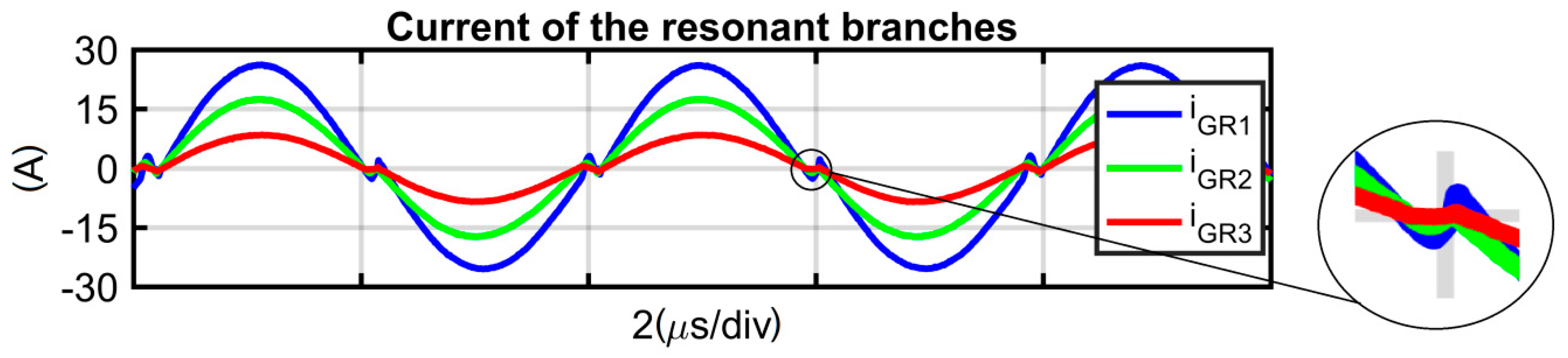
GDT coefficient variation in Equations (2)–(4). The example simulation waveforms of the 5 kW and 500 V/2 kV MRSCC are presented in
Figure 2 and
Figure 3. The results were carried out from two different models and software tools. In the waveforms presented in
Figure 2, during the dead time intervals, the oscillations are halted and the current of the resonant branches equals zero. In this simulation, which was performed in MATLAB/SIMULINK software, all parasitic capacitances of the switches were omitted. In a real circuit (Figure 7a), or precise behavioral simulation model designed for PSpice (
Figure 3), the distortions can be observed in the dead time intervals. The distortions are caused by an interaction of resonant branches and
Coss capacitances of the switches as can be anticipated by comparing the simulation results. Therefore, the distortions in dead time intervals are natural for this topology and are not caused by an improper design of the real converter. For PSpice simulation, the precise models of power transistors provided by the manufactures were used. The simulations parameters are consistent with the experimental setup (
Table 1 and
Table 2) described in
Section 4.
The transition between the boost and buck mode of operation of MRSCC does not require any special control. It depends on the relationships between voltages
Up/
US. The resonant legs should be tuned to achieve the best possible performance of the converter, and only this case is analyzed in the paper. In [
5], the analysis for the general case can be found. For a cost reduction, selected switches can be replaced by diodes, but only unidirectional operation is possible in this case. For example, as presented in the literature [
8], a diode-based ladder resonant switched capacitor converter operates in boost mode only.
3. Coss Losses and Its Reduction by Application of the Commutation Supporting Inductor
The converter operates in ZCS (zero current switch) conditions, but switching losses still occur due to charging and discharging of the output capacitances of the switches. The converter consists of a relatively large number of switches; thus, the switching losses may seriously deteriorate its efficiency, especially under the light load operation.
Coss losses are also the subject of the research presented in [
15,
16], where it is eliminated by the special control of the switches. However, a solution for a converter composed of the number of voltage levels above 2 is not presented.
Coss losses are associated with the energy dispersion from
Coss by the switch that is turned on as well as the power losses during
Coss charging caused by the current flow and commutation in the corresponding switch. In an MOSFET switch, the capacitance
Coss is strongly nonlinear and the charge transferred to
Coss is (from the DC source
UHB, during the lower switch turn on in a half-bridge operating with ZCS):
Typically, both switches in HB are the same type and have the same parameters. Therefore, the high side switch will result in the same charge transfer from a DC source. As a result, the charge
Qoss is transferred twice in the switching period. Thus, the average value of the
Coss losses in a half-bridge of the converter is:
If
Coss capacitances are charged to the certain voltage value in the dead time by the external circuit, the start value in the integral in Equation (6) is a nonzero value. Therefore, the losses (Equation (6)) are lower in such a case, and can even be zero (in idealized analysis). The detailed analysis of
Coss-related energies and losses in HB can found in [
29,
30]. The MRSCC converter consists of
n number of HBs composed with two various types of switches, resulting from their current stresses described by Equations (3) and (4). The total
Coss power loss of the converter is the sum of the
Coss losses of all HBs.
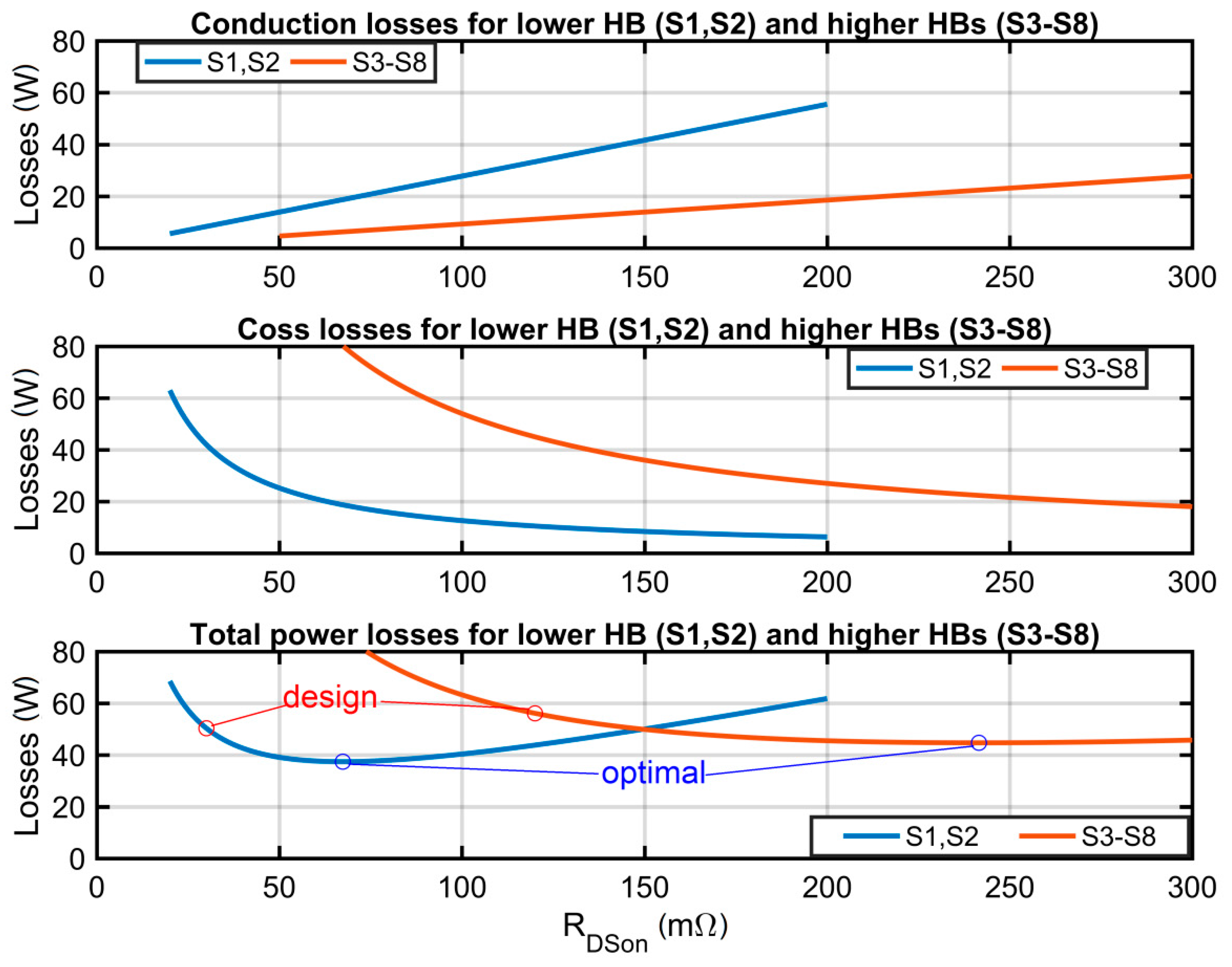
For the analysis and optimization of losses in MOSFET power transistors in MRSCC, the following FOM (figure of merit) [
31] can be used:
where
-turn on resistance of MOSFET,
-charge calculated as in (5) with
UHB =
US.
Based on Equations (3) and (4), the conduction loss in power transistors of the lower HB (S1, S2) and all the higher HBs (S3-S8) can be the following:
where
-on-state resistance of the S1-S2 switches,
-on-state resistance of the S3–S8 switches.
Utilizing Equations (7) and (6), the
Coss loss in power transistors of the lower HB (S1, S2) Δ
PCoss_L and all the higher HBs (S3–S8) Δ
PCoss_H can be found:
where
—on resistance of the S1–S2,
—on resistance of the S3–S8,
—switching frequency,
—figure of merit (7) for S1 and S2,
—figure of merit (7) for S3–S8.
The total power loss for a given group of switches is the sum of the conduction loss and
Coss-related loss. The selection of transistors with higher on-state resistance leads to a higher conduction loss. However, the
Coss loss is lower in such a case, if the figure of merit (Equation (7)) is considered constant. Using the above Equations (8)–(11), it is possible to find the optimal value of
rDSon_L and
rDSon_L for which the total power loss of a transistor is minimal for a given figure of merit. Obviously, the selection of transistors is a discrete problem since only several types of devices with specific parameters are manufactured. The presented solution is continuous, but in spite of this fact, it can be used for the selection of the transistors nearest to the calculated optimal parameters. The optimal on-state resistances of transistors are given by the following relationship:
where
—optimal on resistance of the S1–S2,
—optimal on resistance of the S3–S8,
—switching frequency,
—figure of merit (7) for S1–S2,
—figure of merit (7) for S3–S8,
PS—power of lower voltage side, for which value the minimum losses should occur.
The above Equations (8)–(13) were evaluated for the real setup parameters, which are presented in
Section 4, especially in
Table 1 and
Table 2. The figure of merit was calculated based on Equations (5) and (7) and the
Coss curves from the data sheets for the two transistors selected in the initial design step: SCT3030AL as S1, S2;
FML = 4 nVs and C3M012090D as S3–S8;
FMH = 5.9 nVs. The results are presented in
Figure 4.
As can be observed in
Figure 4, the initially selected transistors are not optimal. However, there is no significant improvement possible since it is about 20% of the total power loss in the switches. A significant improvement of efficiency may be achieved by the introduction of further modifications as described in
Section 4, which nearly eliminates the total
Coss power loss. In case of the initially selected transistors, the
Coss loss accounts for nearly 87% of the total loss in the switches, and in the case of hypothetical optimal switches, 52%. After the introduced modification of the topology, only conduction losses are relevant. The conduction losses are lower for the initially selected transistors (SCT3030AL, C3M012090D) than in the case of any hypothetical optimal ones. Therefore, the initially selected transistors were accepted as the final selection. After the modification, the optimization problem must be defined in another way since there is no longer a tradeoff needed between
Coss and the on-state resistance.
3.1. Concept of MRSCC with Commutation Inductor
To reduce the idle power losses, the topology modification is proposed based on the application of the additional commutation inductor
LSC, which brings a significant reduction to the switching losses. The proposed concept and commutation sequence from odd to even switches is presented in
Figure 5a–c. The inductor
LSC is connected between the output of the lowest HB and the output of the voltage divider created in the lowest voltage level. Due to the fact that all HBs are switched with a 50% duty ratio, the waveform of the current in
LSC is symmetrically triangular with the positive and negative peaks that occur during the commutation. This current charges and discharges the output capacitances of all switches during the commutation, causing ZVS operation.
When all the HBs are turned into
DT mode (
Figure 5b), the output capacitance of all HBs is charged by the current of inductor
LSC (HB1 directly, and the rest via
CCk capacitors). The transition is finished after a certain time, which depends on the peak current of the
LSC and the values of the output capacitances of the switches. To finish the switching sequence, all the even switches are turned on (
Figure 5c). Because the output capacitances of the switches are charged and discharged by an inductor, their switching losses are significantly reduced (in theory it is lossless).
3.2. Application of Communication Capacitors in MRSCC Branches
The resonant branches contain series inductors and therefore, for very short commutation processes, they can be considered as the current sources. The values of those current sources can be assumed equal to the instantaneous current of the resonant branches at the beginning of the commutation. In the precisely tuned circuit, those values are close to zero, which means that the resonant branches have almost no effect on the commutation process. For this reason, the commutation capacitors (relatively small) are applied to the circuit, in parallel to the resonant branches. The commutation capacitors
CCk can be considered as the voltage sources with the value of
US (as well as the all
Ck capacitors). They allow the output capacitances of higher-level HBs to be charged and discharged by the current of the
LSC inductor flow. The inductor
LSC can be considered as the current source with a positive (odd to even switches commutation) or negative (even to odd switches commutation) peak value. The equivalent circuit representing such conditions is shown in
Figure 5d. The circuit can be further simplified, to the circuit where all
Coss are charged in parallel and supplied by one
US voltage source, as shown in
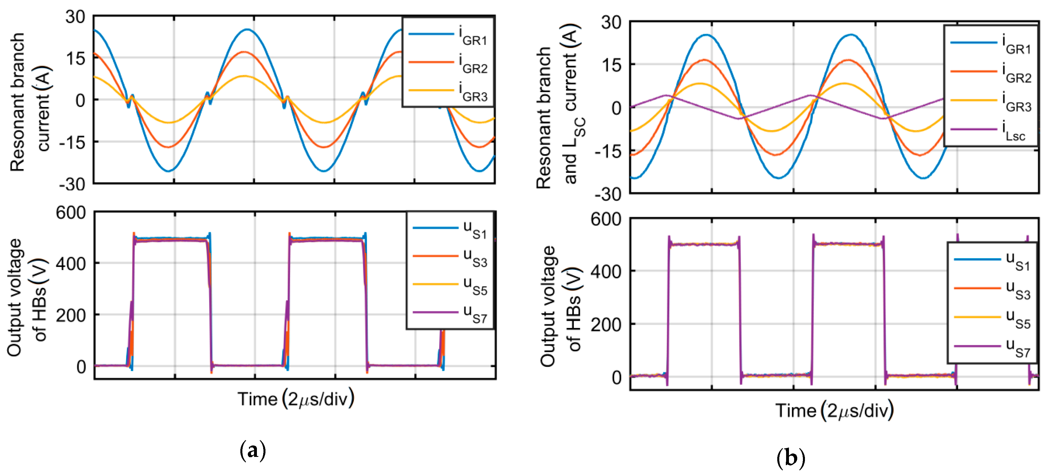
Figure 5e. The application of the commutation capacitors has an additional effect. In the base circuit, during the dead time, the current oscillations in the resonant branches are stopped, thus the resonant frequency of the converter is lower than the resonant frequency of the branches. The commutation capacitors clamp the resonant branches during the dead time, which allows the oscillation to continue. As a result, the resonant frequency of the converter is equal to the resonant frequency of the resonant branches. Furthermore, an additional benefit is the resonant current is a smooth sinusoidal (
Figure 6b), while in the base circuit, some distortion (fast oscillation) can be observed in dead time intervals (
Figure 4 and
Figure 6a). Such distortions reduce the balancing capability of the resonant branches and increase the series-equivalent output resistance of the converter, which will be presented in
Section 4. The application of the
LSC inductor and
CCk capacitors has no direct influence on the voltage gain of the converter. However, it improves the power efficiency and eliminates distortions of the oscillations, resulting in a reduction of the series-equivalent resistance of the converter.
Idle mode losses depend on the peak value of the current of
LSC, which will be demonstrated in
Section 4 together with the research results related to the impact of the
ILSCpk on the switch voltage during commutation. The overall efficiency of the MRSCC is also affected by the remaining switching losses and conduction losses, which are out of the scope of this paper.
3.3. Selection of LSC and CCk Values
Firstly, the required peak current of the
LSC should be determined. According to
Figure 5e, the total charge
QossT that must be provided by the
LSC inductor during the dead time equals the sum of the
Qoss(
Us) determined for every transistor. The charge must be transferred during the dead time interval
tDT, thus the required peak current of
LSC is given as:
where
—charge determined based on Equation (6) for the
m-th transistor for voltage
US.
The required inductance
LSC could be approximated as:
The values of the
CCk capacitors should be large enough so that the voltage across does not change significantly in the dead time interval, when the
ILSC flows through them, charging the
Coss of the transistors. The values of the
CCk capacitors are given by:
where
—change of voltage across
k-th capacitor in the dead time interval.
The selection of the values of the capacitor according to Equation (16) is therefore dependent on the permitted change of the voltage across in the dead time interval ∆UCCk and Coss of the used transistors. Too high ∆UCCk values (too low capacitance of CCk capacitors) cause inefficient charging and discharging of Coss of higher-level transistors and stimulation of resonance branches by voltage glitches during the dead time intervals. Too low ∆UCCk values (too high capacitances) are unfavorable not only in terms of size and cost but also due to the increased participation of these capacitors in energy transport between level voltages, which cause unwanted inrush currents. From the conducted experimental research, it follows that the values of ∆UCCk in the range of few volts (for SiC-based devices between 10 and 100 nF) bring suspected favorable effects. From Equation (16), it follows that the higher the index of the capacitor, the lower the capacitance demanded. To dampen very fast oscillation caused by hard switching of CCk and parasitic inductances, resistors RCk should be added in series with CCk. Typically, values in the range 0.1–1 Ω are optimal.
5. Conclusions
In this paper, the research results under the operation of a modified SiC and Si-based MRSCC converters were presented. The MRSCC converter is a relatively novel topology and its improvement was proposed in this paper. The solution assumes the application of a commutation supporting inductor to reduce the switching losses associated with Coss in a converter made up of any number of levels.
The majority of research was performed in the 5 kW laboratory setup, which demonstrates the feasibility of boost and buck operation of the MRSCC. The conversion between the levels of 500 and 2 kV at a switching frequency 285 kHz, with the use of switches with VDS = 900 and VDS = 650 V, was demonstrated. Both the converters were tested simultaneously in the system with a common high voltage DC link. The input and output of the system remained on a low voltage level, which made it possible to perform high-precision efficiency measurements. Furthermore, it is a good example of a low-cost laboratory test setup for high voltage ratio converters.
The major goal of the research focused on a verification of the topology improvement in a four-level bi-directional MRSCC with a 0.5/2 kV voltage conversion ratio with the use of SiC and Si switches. It was accomplished with very promising results and the following conclusions:
The solution with a commutation supporting inductor in MRSCC is feasible and brings a significant increase of the power efficiency.
A near-total elimination of the Coss power losses was observed in MRSCC with the commutation supporting inductor and the suitable switching applied.
An increase of the voltage efficiency was observed as well (lowering of the output-equivalent series resistance). The voltage gain was more stable vs. load and the difference between the theoretical and practical voltage gain was lower than in the case without the proposed improvements.
The method is very efficient in MRSCC with Si MOSFET as well. Through the application of the commutation supporting inductor, the performance measured in the case of the Si MOSFET MRSCC increased to the level comparable with the converter based on outstanding SiC switches.
In the SiC-based MRSCC, a high power efficiency of 98.5% was measured.
The efficiency versus power characteristic showed an insignificant decline when the power increased, which is also beneficial. The voltage drop versus power was not significant in the demonstrated design cases of MRSCC. The best solution of 2.5% of the voltage decrease in the 5 kW range was observed. The results of the heat distribution in the converter showed that it can be regular. Overheating of particular cells was not observed.


