Article

Analysis and Design of Coupled Inductor for Interleaved Buck-Type Voltage Balancer in Bipolar DC Microgrid

Department of Electrical and Computer Engineering, Sungkyunkwan University, Suwon 16419, Korea
*
Author to whom correspondence should be addressed.
Energies 2020, 13(11), 2775; https://doi.org/10.3390/en13112775
Submission received: 15 April 2020 / Revised: 22 May 2020 / Accepted: 26 May 2020 / Published: 1 June 2020
(This article belongs to the Section A1: Smart Grids and Microgrids)

Abstract

:
A voltage balancer (VB) can be used to balance voltages under load unbalance in either a bipolar DC microgrid or LVDC (Low voltage DC) distribution system. An interleaved buck-type VB has advantages over other voltage balance topologies for reduction in output current ripple by an aspect of configuration of a physically symmetrical structure. Similarly, magnetic coupling such as winding two or more magnetic components into a single magnetic component can be selected to enhance the power density and dynamic response. In order to achieve these advantages in a VB, this paper proposes a VB with a coupled inductor (CI) as a substitute for inductors in a two-stage interleaved buck-type VB circuit. Based on patterns of switch poles under load variation, the variation in inductor currents under four switching patterns is induced. The proposed CI is derived from self-inductance based on the configuration structure that has a two-stage interleaved buck type and mathematical design results based on the coupling coefficient, where the coupling coefficient is a key factor in the determination of the dynamic response of the proposed VB in load variation. According to the results, a prototype scale is implemented to confirm the feasibility and effectiveness of the proposed VB.

1. Introduction

A microgrid system is an important eco-friendly distribution system that allows for high efficiency and flexible integration of distributed generations and energy storage systems [1]. Among major distributed generation systems, photovoltaic systems and energy resources connected to batteries have DC output. Thus, connection between a DC microgrid and distributed generation system can result in enhanced efficiency, grid performance, and overall energy flexibility of the distribution system [2,3,4]. Moreover, the advantages of DC distribution systems over AC distribution systems include the simple control scheme without reactive power and frequency coordination [5,6]. A typical configuration of a unipolar and bipolar DC microgrid is shown in Figure 1. The main configuring converter is given respectively with a single AC/DC converter topology or converter-based topologies, namely a voltage balancer (VB). The aims of these converters are to interface and regulate DC bus voltage. However, power fluctuations in renewable energy or load variations in the DC microgrid can cause power surges, as they cause voltage fluctuations in voltage buses. The voltage fluctuation of DC links has highlighted not only a unipolar DC microgrid but also a bipolar DC microgrid. According to the literature, a voltage regulation method for a DC bus, based on control modeling such as droop or hierarchical control, is proposed to compensate voltage variation [7,8,9]. Similarly, interlinking converters are analyzed in order to compensate for voltage drop in an AC/DC hybrid microgrid [10].
The major aspects in these studies are associated with bus configuration with unipolar voltage and voltage regulation using a single AC/DC converter topology, whereas single-input series-output voltage source converters (SISO VSCs) or VBs are configured in order to form a bipolar DC microgrid. These two topologies can be determined based on a selected reference voltage of poles (e.g., High Voltage DC, HVDC or Low Voltage DC, LVDC). Generally, a SISO VSC is used in a HVDC system. On the other hand, VBs are commonly used to form a bipolar DC bus and to achieve stable voltage balance, where the VB has the advantage of simple structure and lower cost compared to SISO VSCs [11]. As a result, several effective VB circuits based on a DC/DC converter circuit have been developed and analyzed to form a unipolar low-voltage DC microgrid and balance voltage [12,13].
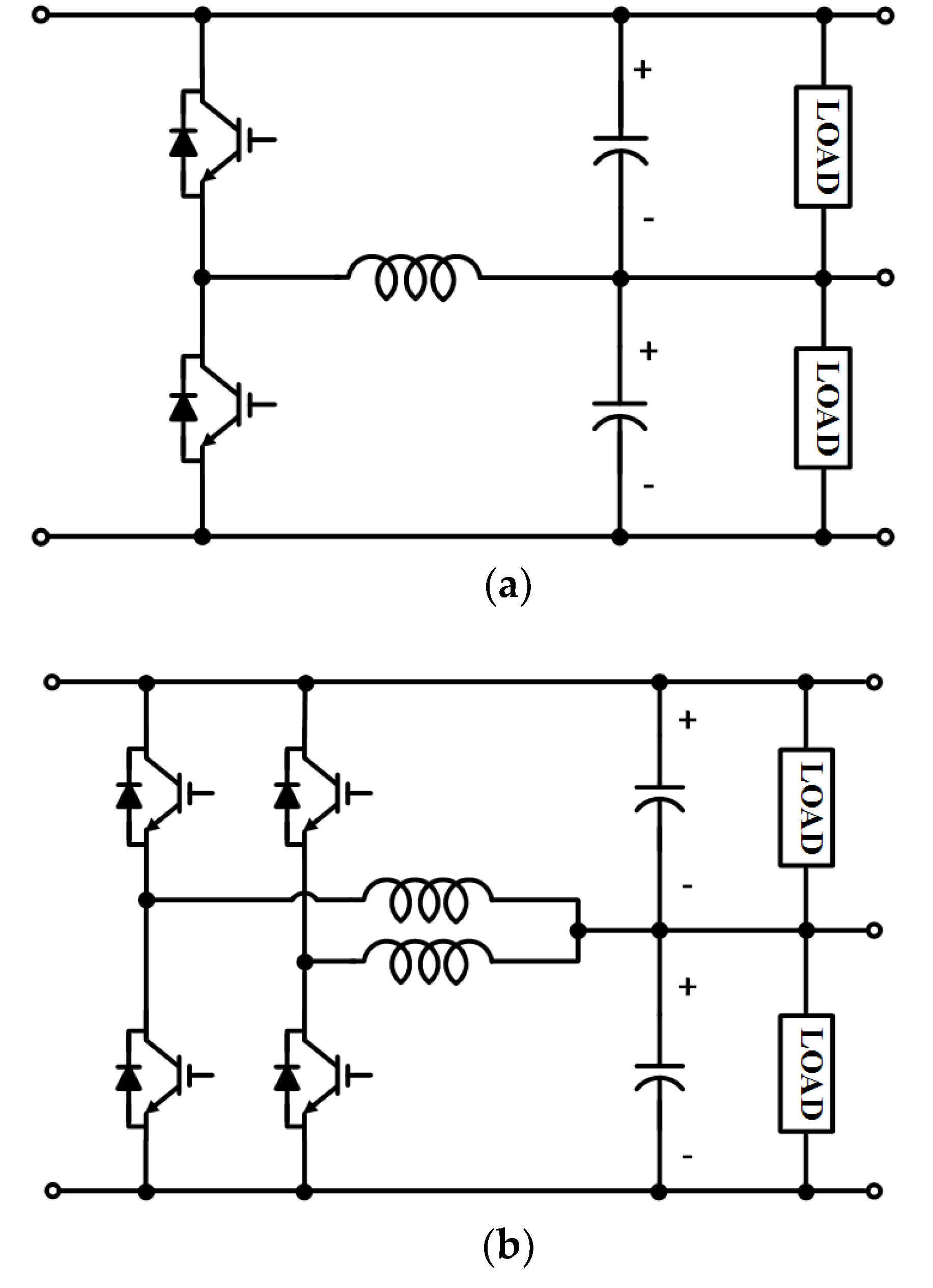
In [12], a VB based on a bi-directional DC/DC boost converter is proposed. The purpose of this topology is to boost voltage and balance the voltage difference between the positive and negative voltage buses. Thus, this topology is only suitable for step-up and bi-direction power flow application. In [13], a half-bridge VB, as in Figure 2a, is presented. Circuit configuration is based on a buck converter, which is significantly superior in regard to having less components such as switches and passive elements. However, a half-bridge VB uses only one inductor, resulting in a relatively high inductor current ripple. Thus, this causes increased inductance, and a higher inductance also causes a less dynamic response. In order to mitigate the drawbacks above, an interleaved-type VB is proposed in [11] and shown in Figure 2b. An interleaved-type VB has an advantage over the half-bridge type mentioned above. The interleaved type of buck converter is selected based on high power density, current distribution, and dynamic response. Therefore, an interleaved-type VB is best suited to compensate drawbacks of the half-bridge type. However, as the stage of the interleaved topology increases, the magnetic component increases accordingly. As such, the increased magnetic component still poses a disadvantage in terms of the magnetic size. In regard to the interleaved circuit, a coupled inductor (CI) can be chosen in terms of integrated magnetic design. In numerous literatures, the CI is a solution in the optimization of two or more inductors [14,15]. Based on the concept of the interleaved buck-type DC/DC converter with distribution of the inductor current and integrated magnetic components, this paper proposes an interleaved buck-type VB with CI. This configuration has an advantage that each phase of the CI is overlapped in order to reduce the overall output current. Moreover, the CI has the advantage to improve the dynamic response of interleaved voltage regular modules [16]. Therefore, when designing a coupled inductor, an appropriate coupling coefficient selection technique is required. This paper is organized as follows:
The overall summary of the paper is as follows: In Section 2, the interleaved buck-type voltage balancer with CI is introduced. Section 3 presents the operations of the VB classified into four switching modes under voltage-unbalanced conditions caused by load variation, and the inductor current variation is induced by operation modes. After that, the coupling coefficient is considered, which is determined based on the results of describing current variation, where the coupling coefficient is one of the factors that come from current dynamic response of the voltage balancer [17]. According to the voltage drop conditions, the proposed voltage balancer operation of three voltage compensation modes is described. The simulation results and experimental results are presented in Section 4 and Section 5, respectively, in order to validate the proposed voltage balancer. Finally, experimental results are presented to prove the validity of analysis results.

2. Proposed Interleaved Buck-Type VB with Two-Phase CI

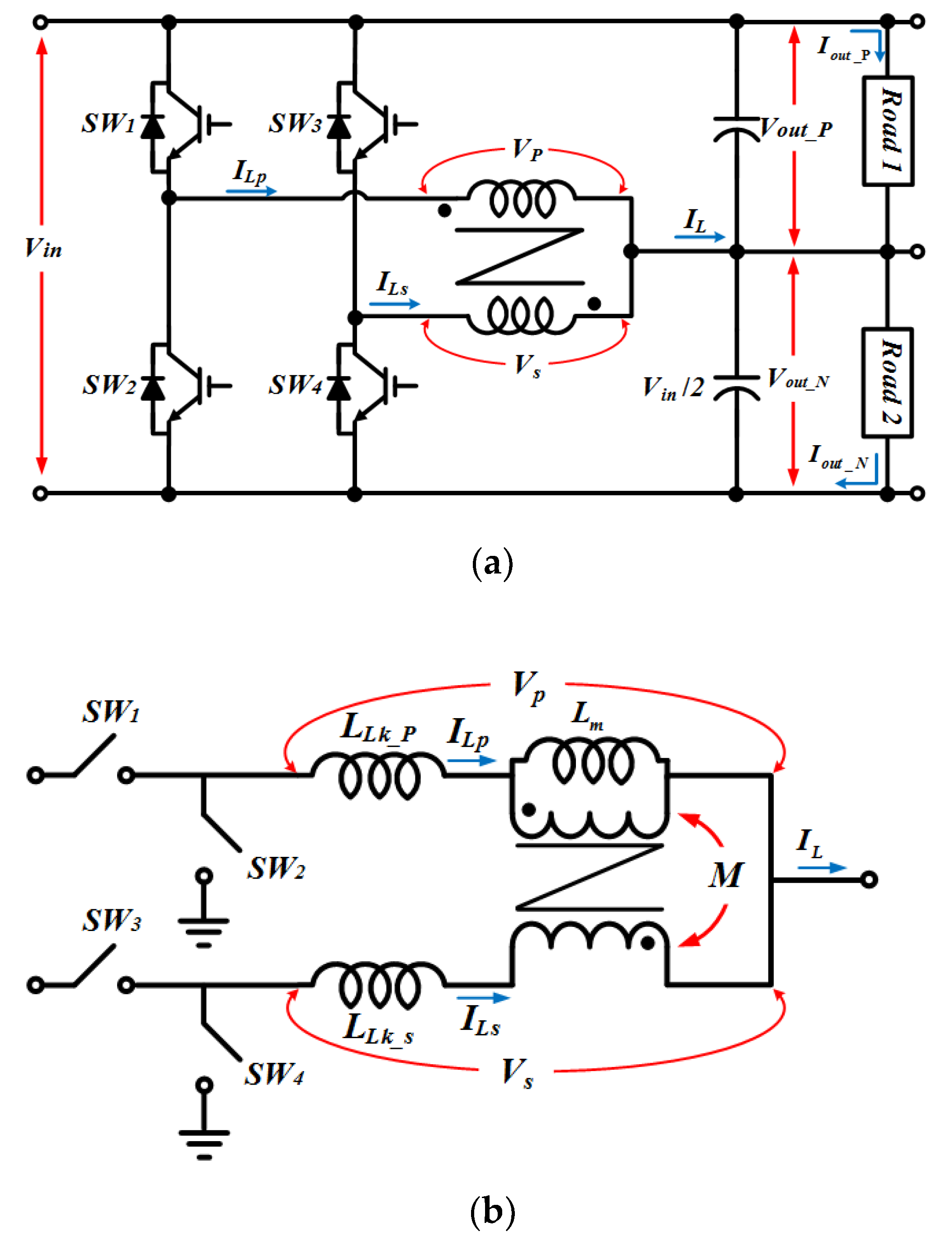
This section describes the circuit configuration of the proposed VB and several assumptions to ease the analysis of the CI. Figure 3 shows the circuit of the proposed interleaved buck-type VB with the CI, where Vout_P and Vout_N are the positive bus voltage and negative bus voltage, respectively. As highlighted in Section 1, the CI in this paper is adopted in a two-stage interleaved voltage balancer, which is similar to the circuit configuration of the interleaved buck converter. Therefore, each switch pole in the proposed VB operates 180° out of phase. In Figure 3a, the VB consists of an interleaved buck converter-based configuration, where the two inductors are substituted by a two-phase CI.
In Figure 3b, the utilized CI has an inverse coupling consisting of a leakage inductance of primary side LLk_p, leakage inductance of secondary side LLk_s, magnetizing inductance Lm, and ideal transformer. The mathematical relation between each inductance is determined as follows:
L L k _ p = ( 1 k 2 ) L p
L m = k 2 L p
where Lp is the self-inductance of the primary side and k is the coupling coefficient of the CI. LLk_P and LLk_N are designed as inductors with one magnetic component. Therefore, this configuration has numerous advantages such as increasing power density, reducing the number of magnetic components, and optimizing the volume of the VB. The VB regulates the output voltage regularly to Vin/2 under voltage control mode. The switches of each pole operate contemporarily by turning on and off, and the duty cycle is restricted by half when the VB operates in steady-state operation. Consequently, the stored energy in the CI is transferred to the neutral line in the bipolar DC microgrid, where the inductor current ILp and ILs is overlapped in IL.
On a balanced load condition, the total inductor current, IL, is zero, while IL has different values under an unbalanced load condition. For ease in analyzing the utilized CI, the following assumptions are considered:
(1)
The CI is modeled as an ideal transformer, which has a turns ratio of 1:1, magnetizing inductor, and leakage inductor. The winding resistance is neglected.
(2)
The proposed VB is operated only under continuous conduction mode (CCM), and the corresponding values of each air gap area, cross section, and air gap length in the two-phase CI have similar values.
(3)
The equations can be applied respectively to the primary and secondary windings of the CI. In this paper, the following equations are derived for the primary winding.
Based on these assumptions, Vp and Vs applied to each winding in a two-phase inverse CI can be expressed by the following equation, which is known simple circuit theory [18]:
V p = L p d i L p d t M d i L s d t
V s = L s d i L s d t M d i L p d t
where M is mutual inductance, and the self-inductance of each winding is indicated as Lp and Ls. Considering the above assumptions, Lp and Ls can be considered to have equal inductance. In addition, the relationship between M and self-inductance is commonly represented as below.
L p = L s = L
M = k L p L s = k L
where k is the coupling coefficient. From (5) and (6), (3) and (4) are rearranged as follows.
V p = L d i L p d t k L d i L s d t
V s = L d i L s d t k L d i L p d t
(8) can be rearranged as the current variation of the primary side.
d i L s d t = ( V s + k L d i L p d t ) 1 L
Substituting (9) into (7), Vp is given as in (10). Similarly, Vs can be expressed as (11) from the above-derived equations.
V p = L d i L p d t k 2 L d i L p d t k V s
V s = L d i L s d t k 2 L d i L s d t k V p

3. Switching Operation

3.1. Analysis of Switching Mode under Unbalanced Load Condition

In this part, four switching modes in operation of the proposed VB is employed. As previously highlighted, the analysis for operation modes is similar to buck converter operation. Figure 4 illustrates the switching of patterns, which is classified by the steady and transient state of the proposed VB. Proposed VB operation is considered as an operation mode starting from mode 1 to mode 4. The four operation modes are indicated. When the VB operates in the steady state, the switch duty cycle is restricted by half, and the switches of each pole operate complementarily, as shown in Figure 4a,b. However, when the VB operates in the transient state, such as load variation in the DC micro grid, the switch duty varies slightly. From the changed duty, the top switches or the bottom switches are turned on and off simultaneously, as in Figure 4c,d. These changes of switch operation occur temporarily when the load is changed. Further details of the analysis of the four modes and current flow path are presented as follows:
  • Mode 1
    Switch SW1 and SW4 are turned on, and the current ILp that flows through the leakage inductor (Lp) increases. Conversely, when SW2 and SW4 are turned off, the current ILs that flows through the leakage inductor Ls decreases. In Mode 1, the duty of each switching pole is restricted by half of duty.
  • Mode 2
    This operating mode is similar to that in Mode 1, where the switching pattern of Mode 2 is contrary to Mode 1. SW2 and SW3 are turned on and ILs that flows through Ls increases, whereas ILp decreases.
  • Mode 3
    In mode 3, the currents ILp and ILs begin to increase due to increased load variation when SW1 and SW2 are turned on. Vin stores energy through Lp and Ls, and inductive current rises linearly. In summary, this mode shows up through duty variation between mode 1 and mode 2.
  • Mode 4
    In mode 4, the currents ILp and ILs begin to decrease due to decreased load variation. Contrary to Mode 3, SW1 and SW3 are turned off. Conversely, SW2 and SW4 are turned on.

3.2. Analysis of Swtiching Patterns Under Transient State

Based on switching patterns, the key waveforms of the CI are described in this part. Figure 5 and Figure 6 illustrate the operating waveforms according to the switching scheme. Regarding switching patterns of the proposed VB, there are two distinct operation states: Steady state and transient state. The steady state operation during one switching cycle is illustrated as in Figure 5. In addition, the transient state operation can be divided into two patterns, as presented in Figure 6, where it illustrates increased or decreased variation of ΔiL in Mode 3 and Mode 4. The major representations are summarized as follows: ΔiL_Mode_n denotes the current variation in each switch operation from mode 1 to mode 4, and ΔiL_Pattern_n is the current change based on these switching patterns. The basic equations corresponding to current variation are expressed as (12) and (13).
d i L p d t = 1 + k V L s V L p ( 1 k 2 ) L V L p
d i L s d t = 1 + k V L p V L s ( 1 k 2 ) L V L s
When VB operates in the steady state, the switch duty cycle is restricted by half. Consequently, the switch states repeat Mode 1 and Mode 2. The basic current variation equation corresponding to the operation modes are expressed as follows.
Δ i L _ Mode n = ( 1 + k V L 2 V L 1 ) ( 1 k 2 ) L V L 1 D T s
Based on (14), equations of current variation under mode 1 and mode 2 can be given as (15) and (16), respectively:
Δ i L _ Mode 1 = ( 1 k ) V p ( 1 k 2 ) L D T s = V p ( 1 + k ) L D T s = ( V i n V o u t _ N ) ( 1 + k ) L D T s
Δ i L _ Mode 2 = ( 1 k ) V s ( 1 k 2 ) L D T s = V s ( 1 + k ) L D T s = ( V o u t _ N V i n ) ( 1 + k ) L D T s
As observed in Figure 4, upper switches of each switching pole are either turned on or turned off in a short span. At the initial time of the unbalanced load such as load increase, the switch duty cycle changes by duty cycle variation ΔD, which lasts for a short time. As a result, the switch states shift from Figure 5 to Figure 6 according to the load variation condition. The corresponding equations of mode 3 and 4 can be expressed similarly.
Δ i L _ Mode 3 = 2 ( V i n V o u t _ N ) ( 0.5 Δ D ) T s ( 1 k ) L
Δ i L _ Mode 4 = 2 V o u t _ N ( 0.5 Δ D ) T s ( 1 k ) L
Based on the patterns from 1 to 3, ΔiL_Pattern_1~3 can be obtained respectively as
Δ i L _ Pattern 1 = Δ i L _ Mode 1 + Δ i L _ Mode 2 = V p ( 1 + k ) L D T s + V s ( 1 + k ) L D T s
Δ i L _ Pattern 2 = Δ i L _ Mode 1 + Δ i L _ Mode 2 + 2 Δ i L _ Mode 3 = V p ( 1 + k ) L D T s + V s ( 1 + k ) L D T s + 4 ( V i n V o u t _ N ) ( 0.5 Δ D ) T s ( 1 k ) L
Δ i L _ Pattern 3 = Δ i L _ Mode 1 + Δ i L _ Mode 2 + 2 Δ i L _ Mode 4 = V p ( 1 + k ) L D T s + V s ( 1 + k ) L D T s 4 V o u t _ N ( 0.5 Δ D ) T s ( 1 k ) L
In the above equations, ΔiL_Pattern_1~3 are changed by k, which means that the current dynamic response of the CI could be determined by k. In other words, the performance of the VB is affected by the value of k. Figure 7 shows the relationship between k and current variation. In Figure 7a, ΔiL_Pattern2 increases significantly with an increase in k. A different current variation curve with respect to different k is shown in Figure 7b. These figures indicate that an increase in k results in more current variation in a small duty variation ΔD, and the value of ΔiL_Pattern_n can be changed by k. Hence, it can be concluded that the value of k should be selected largely in this paper. In addition, the current variation of the total inductor current is similar to the above figures. Figure 7c indicates IL waveforms compared to k under load variation. To sum up the whole results, it was confirmed that the larger the value of the coupling coefficient, the better improved the dynamic response of the inductor current.

4. Simulation Results

4.1. Comparison of Inductance and Dynamic Response of CI

In this section, the inductance between coupled type and non-coupled type is compared. From (15), the self-inductance of coupled type LCI can be calculated as follows.
L C I = V i n V o u t _ N ( 1 + k ) Δ i L _ Mode 1 D T s = ( 760 380 ) ( 1 + 0.9 ) × 4 × 0.5 × 50 × 10 6 = 1.25 mH
where it is assumed that the coupling coefficient is 0.9, switching frequency is 20 kHz, rated current of each winding of the coupled inductor is 10 A, and current ripple is 40%. According to (1) and (2), LLk_P and Lm can be calculated as (23) and (24), respectively.
L L k _ P = ( 1 k ) L C I = ( 1 0.9 ) × 1.25 m H = 125 μ H
L m = k × 1.25 m H = 0.9 × 1.25 m H = 1.125 mH
Based on the above calculation process, the self-inductance of a non-coupled configuration such as the half-bridge-type VB can be calculated as (25).
L N C = V i n V o u t _ N Δ i L _ Mode 1 D T s = ( 760 380 ) 4 × 0.5 × 50 × 10 6 = 2.375 mH
From (22) and (25), it can be proven that the self-inductance of the non-coupled configuration is greater than that of the coupled configuration as the current ripple is proportional to the total inductor current ripple. This can be adopted to optimize inductor volume.

4.2. Performance Characteristic under Load Variation

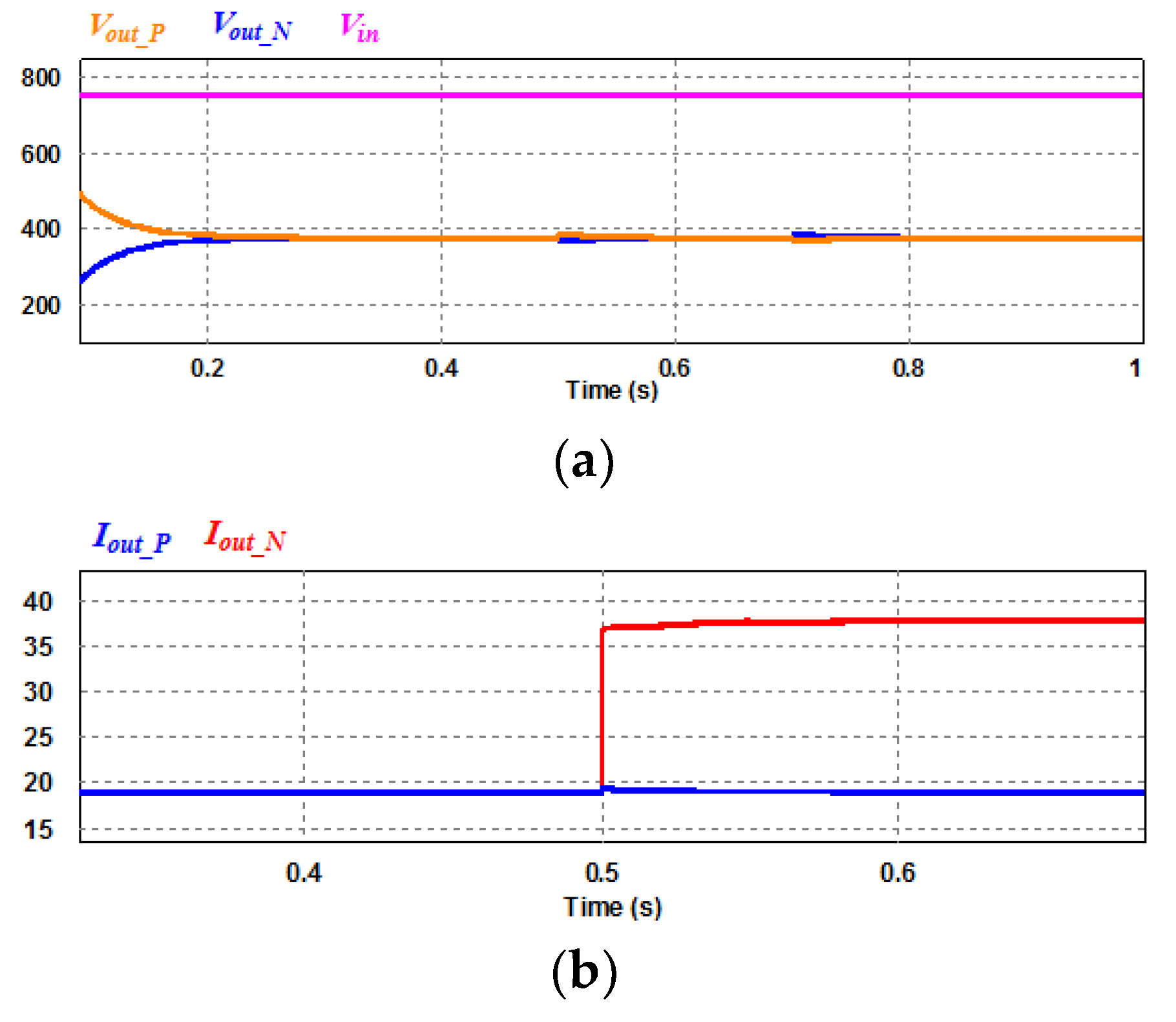
To verify the effectiveness of voltage balancing under the load variation condition, the proposed VB is simulated in PSIM software. The detailed parameters for the simulation condition are listed in Table 1. As highlighted in Section 3.2, k should be considered as a value close to 1. Therefore, the value of k is selected as 0.9. More detailed parameters for CI are listed in Table 2, where the value of self-inductance is calculated by (22). The conditions of load variation are listed in Table 3, where only the load linked to the negative voltage pole is considered. Therefore, R2 is changed at a specific time to investigate the balanced voltage. Along with simulation parameters and scenario, simulation results of the voltages and currents are shown in Figure 8. In Figure 8a, two DC bus voltages, Vout_P and Vout_N, are balanced under two load variation conditions. The load value R2 connected to the negative voltage pole is changed from 20 to 10 Ω at t = 0.5 s as Figure 8b, and from 10 to 20 Ω at t = 0.7 s as Figure 8c.
Figure 9a,b are respectively waveforms of IL, which is the total inductor current of the CI, and Figure 9c,d are respectively current waveforms under the balanced load condition and unbalanced load condition. As a result of the simulation, the validity of constant voltage control of the bipolar voltage buses with the proposed VB is verified.

5. Experiment Results

Based on simulation results, a prototype scale has been built. Test conditions and detailed parameters are listed respectively in Table 4 and Table 5, where the reference voltage of the positive and negative bus is 190 V and the input voltage is 380 V. To configure the two-phase CI, an EE ferrite core is used. A structure and prototype scale of the CI is shown in Figure 10, which specifies a magnetizing inductance of 644 µH. In addition, a prototype scale CI has a small amount of different values between two leakage inductances LLk_p and LLk_s because of windings and other minor differences.
Figure 11 shows the operating waveforms of voltages and inductor currents under a balanced load. This figure indicates the balancing capability of the proposed VB under the before-load-variation condition, where Vout_N regulates as 190 V, which is half of Vin. Figure 11a shows waveforms of Vout_N and IL under the load variation condition with increasing load and decreasing load variation at a specific time. In each condition, IL varies by the load variation condition. Figure 11b shows the waveforms of Vin, Vout_N, ILp, and ILs under a balanced load, and Figure 11c is the enlarged waveform of inductor currents. In this figure, inductor currents ILp and ILs show a 180° phase delay, and the sum of currents is nearly zero.
Figure 12 shows waveforms of the output voltages, inductor current, and load current under the load unbalanced condition with increasing load variation. In Figure 12a, load variations occur from 62.1 to 36.8 Ω onto the negative voltage bus. Despite increased load variation, bi-polar voltage buses are controlled at the reference voltage. Figure 12b shows inductor current waveforms, which indicate similarly in the balanced load condition, but the sum of the current is not zero, because of the load difference.

6. Conclusions

This paper proposes a VB with a two-phase CI. An interleaved-type buck converter circuit and magnetic coupling design is considered in an aspect of enhanced power density and reduced current ripple as a substitute for two inductors in an interleaved buck-type circuit. In order to design the CI, four switching operation modes of the proposed VB under a load variation condition are defined. In addition, switching patterns are analyzed to quantize the overall inductor current variation. The analyzed results indicate that the designed coupling coefficient value leads to an inductor current magnitude and dynamic response of the CI. The validity of the deduced results is confirmed by using MATLAB. As a result of this, a coupling coefficient k, which has a large value under 1, as nearby as possible is selected. Though leakage inductances are decreased and current ripples in each phase in the CI are increased by the selected k value, the overall output current can be overlapped because of a physically symmetrical circuit structure. Therefore, a current ripple reduction effect can be obtained with less inductance. The effectiveness of the proposed interleaved-type VB with the coupled inductor is verified through simulation and experimental results. In the experimental configuration, the VB with the CI deployment of the small-scale prototype is implemented. These results indicate the maintenance of voltage balancing under the fluctuation condition of the load connected to the negative voltage pole in the bipolar DC microgrid. Considering the implemented prototype scale VB, it is necessary in future work to verify the effectiveness of the full-scale VB suitable for a practical DC microgrid.

Author Contributions

J.-m.P. conceived and designed the experiments; J.-m.P. and H.-j.B.; performed the experiments, S.-h.K. and B.-j.K.; analyzed the data and contributed simulation tools, J.-m.P. and C.-y.W.; wrote the paper, C.-y.W. participated in research plan development and revised the manuscript. All authors have contributed substantially to the manuscript. All authors have read and agreed to the published version of the manuscript.

Funding

This research was funded by Korea Institute of Energy Technology Evaluation and Planning (KETEP) (No. 20184030202190).

Acknowledgments

This work was supported by “Human Resources Program in Energy Technology” of the Korea Institute of Energy Technology Evaluation and Planning (KETEP), granted financial resource from the Ministry of Trade, Industry & Energy, Republic of Korea. (No. 20184030202190).

Conflicts of Interest

The authors declare no conflict of interest.

References

  1. Kwasinski, A.; Onwuchekwa, C.N. Dynamic behavior and stabilization of dc microgrids with instantaneous Constant-Power loads. IEEE Trans. Power Electron. 2010, 26, 822–834. [Google Scholar] [CrossRef]
  2. Mohammadi, J.; Ajaei, F.B.; Stevens, G. Grounding the DC microgrid. IEEE Trans. Ind. Appl. 2019, 55, 4490–4499. [Google Scholar] [CrossRef]
  3. Kumar, D.; Zare, F.; Ghosh, A. DC microgrid technology: System architectures, AC grid interfaces, grounding schemes, power quality, communication networks, applications, and standardizations aspects. IEEE Access 2017, 5, 12230–12256. [Google Scholar] [CrossRef]
  4. Anand, S.; Fernandes, B.G.; Guerrero, J.M. Distributed control to ensure proportional load sharing and improve voltage regulation in Low-Voltage DC microgrids. IEEE Trans. Power Electron. 2012, 28, 1900–1913. [Google Scholar] [CrossRef] [Green Version]
  5. Che, L.; Shahidehpour, M.; AlAbdulwahab, A.; Al-Turki, Y. Hierarchical coordination of a community microgrid with ac and dc microgrids. IEEE Trans. Smart Grid 2015, 6, 3042–3051. [Google Scholar] [CrossRef]
  6. Roldán-Porta, C.; Roldán-Blay, C.; Escrivá-Escrivá, G.; Quiles, E. Improving the sustainability of Self-Consumption with cooperative DC microgrids. Sustainablity 2019, 11, 5472. [Google Scholar] [CrossRef] [Green Version]
  7. Han, Y.; Ning, X.; Yang, P.; Xu, L. Review of power sharing, voltage restoration and stabilization techniques in hierarchical controlled DC microgrids. IEEE Access 2019, 7, 149202–149223. [Google Scholar] [CrossRef]
  8. Liu, S.; Li, Z.; Liu, W.; Liu, X. Multi-Level bus voltage compensation of droop control with enhanced Load-Sharing capability for DC microgrid. J. Eng. 2019, 2019, 3056–3061. [Google Scholar] [CrossRef]
  9. Gao, F.; Bozhko, S.; Asher, G.; Wheeler, P.; Patel, C. An improved voltage compensation approach in a Droop-Controlled DC power system for the more electric aircraft. IEEE Trans. Power Electron. 2015, 31, 7369–7383. [Google Scholar] [CrossRef]
  10. Loh, P.C.; Li, D.; Chai, Y.K.; Blaabjerg, F. Autonomous control of interlinking converter with energy storage in hybrid AC–DC microgrid. IEEE Trans. Ind. Appl. 2013, 49, 1374–1382. [Google Scholar] [CrossRef]
  11. Wang, F.; Lei, Z.; Xu, X.; Shu, X. Topology deduction and analysis of voltage balancers for DC Micro-Grid. IEEE J. Emerg. Sel. Top. Power Electron. 2016, 5, 672–680. [Google Scholar] [CrossRef]
  12. Tavakoli, S.D.; Sheshyekani, K.; Khajesalehi, J.; Hamzeh, M. Decentralised voltage balancing in bipolar dc microgrids equipped with Trans-Z-Source Interlinking converter. IET Renew. Power Gener. 2016, 10, 703–712s. [Google Scholar] [CrossRef]
  13. Han, B. A Half-Bridge voltage balancer with new controller for bipolar dc distribution systems. Energies 2016, 9, 182. [Google Scholar] [CrossRef]
  14. Wai, R.; Liaw, J. High-Efficiency Coupled-Inductor-Based Step-Down converter. IEEE Trans. Power Electron. 2016, 31, 4265–4279. [Google Scholar] [CrossRef]
  15. Wu, H.; Lu, J.; Shi, W.; Xing, Y. Nonisolated bidirectional DC–DC Converters with Negative-Coupled inductor. IEEE Trans. Power Electron. 2011, 27, 2231–2235. [Google Scholar] [CrossRef]
  16. Yang, F.; Ruan, X.; Yang, Y.; Ye, Z. Interleaved critical current mode boost PFC Converter with coupled inductor. IEEE Trans. Power Electron. 2011, 26, 2404–2413. [Google Scholar] [CrossRef]
  17. Tavakoli, S.D.; Zhang, P.; Lu, X.; Hamzeh, M. mutual interactions and stability analysis of bipolar DC microgrids. CSEE J. Power Energy Syst. 2019, 5, 444–453. [Google Scholar]
  18. Zhu, G.; McDonald, B.A.; Wang, K. Modeling and analysis of coupled inductors in power converters. IEEE Trans. Power Electron. 2010, 26, 1355–1363. [Google Scholar] [CrossRef]
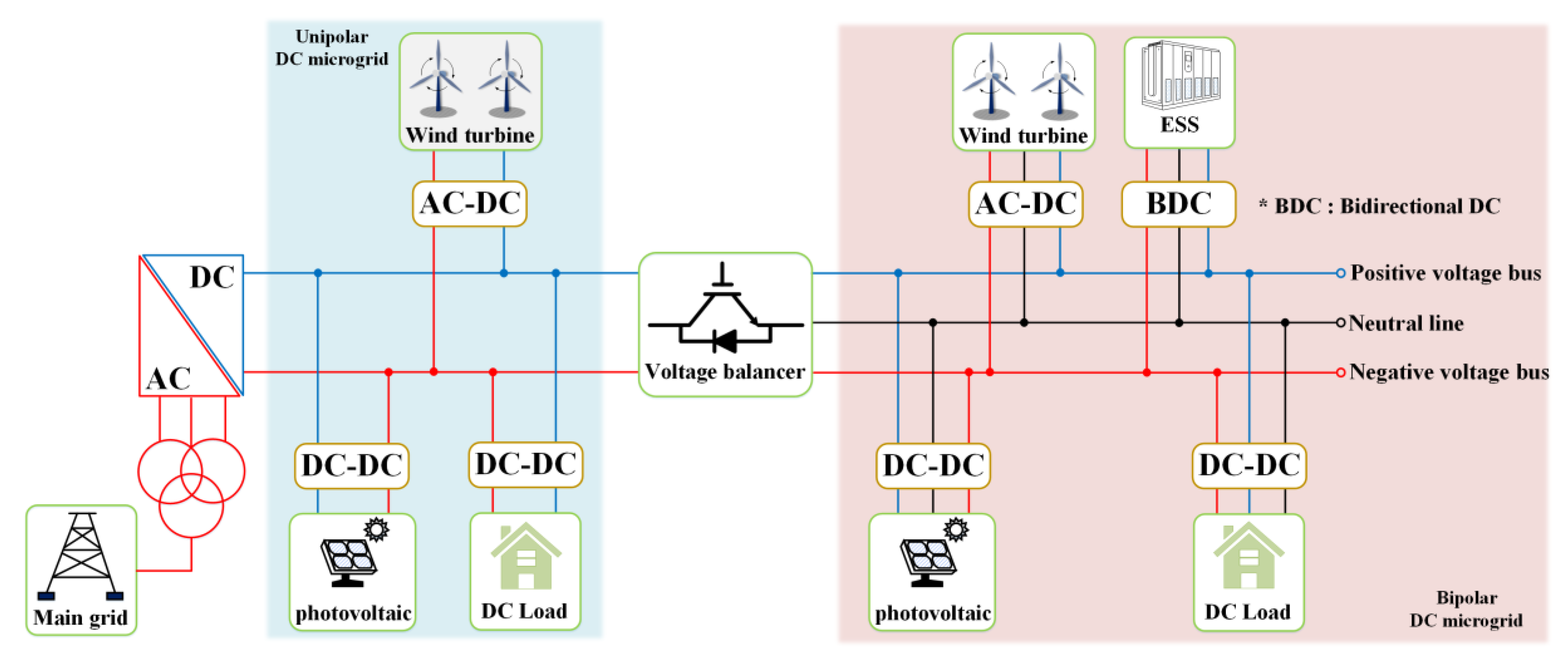
Figure 1. Block diagram of DC microgrid based on unipolar and bipolar voltage bus.
Energies 13 02775 g001
Figure 2. The circuit configuration of early proposed voltage balancer (VB): (a) Half-bridge type; (b) interleaved buck type.
Energies 13 02775 g002
Figure 3. Configuration of DC microgrid with VB and coupled inductor (CI): (a) Proposed VB; (b) equivalent schematic of two-phase CI.
Energies 13 02775 g003
Figure 4. Switching patterns and current flow path of the proposed VB: (a) Mode 1; (b) Mode 2; (c) Mode 3; (d) Mode 4.
Energies 13 02775 g004
Figure 5. Switching scheme of proposed VB under pattern 1; steady state.
Energies 13 02775 g005
Figure 6. Switching scheme of proposed VB under loads condition: (a) Pattern 2: Unbalanced load (increased loads of negative voltage pole); (b) pattern 3: Unbalanced load (decreased loads of negative voltage pole).
Energies 13 02775 g006
Figure 7. Inductor current variation by coupling coefficient: (a) Current variation curves with different coupling coefficients and duty ratios in switching pattern 2, (b) comparison of different coupling coefficients in operation mode 3, (c) current variation curves of total inductor current with different coupling coefficients.
Energies 13 02775 g007
Figure 8. Simulation waveforms under load variation conditions: (a) Waveforms of input and output DC bus voltages during the whole simulation time; (b) waveforms of load currents at unbalanced load (increased load), (c) waveforms of load currents at unbalanced load (decreased load).
Energies 13 02775 g008aEnergies 13 02775 g008b
Figure 9. Simulation waveforms of inductor currents: (a) Waveforms of total inductor currents at unbalanced load (increased load), (b) waveforms of total inductor currents at unbalanced load (decreased load), (c) enlarged waveforms under balanced load, (d) enlarged waveforms under unbalanced load.
Energies 13 02775 g009
Figure 10. Structure of two-phase CI using EE core: (a) the EE core structure and windings of CI, (b) the experimental prototype of CI.
Energies 13 02775 g010
Figure 11. Experimental waveforms under balanced load condition: (a) Waveforms of input voltage, negative pole voltage, and total inductor current, (b) waveforms of negative pole voltage and inductor currents under balanced load condition, (c) enlarged waveforms of inductor currents.
Energies 13 02775 g011
Figure 12. Experimental waveforms under unbalanced load condition: (a) Input voltage, negative pole voltage, and load currents; (b) inductor currents of each winding.
Energies 13 02775 g012
Table 1. Simulation parameters.
ParameterValue
Vin760 V
Reference voltage Vout_P and Vout_N380 V
Initial value of R1 and R2 20 Ω
Table 2. Parameters for two-phase CI.
ParameterValue
k0.9
L1.25 mH
Lm1.125 mH
LLk_p and LLk_s125 µH
Switching frequency20 kHz
Table 3. Load variation conditions.
ParameterDescription
Load variation of R220 Ω ↔ 10 Ω
0 ~ 0.49 sBalanced load
0.5 ~ 0.69 sUnbalanced load (increased load)
0.7 ~ 1 sUnbalanced load (decreased load)
Table 4. Experimental parameters.
ParameterValue
Vin380 V
Reference voltage Vout_P and Vout_N190 V
Rated power1.6 kW
Initial value of R1 and R2 62.7 Ω and 62.1 Ω
Load variation of R262.1 Ω ↔ 36.8 Ω
Table 5. Parameters for two-phase CI.
ParameterValue
k0.95
Lm644 µH
LLk_p and LLk_s68 µH
Switching frequency20 kHz
Core sizeEE 7066