Derivation of OCC Modulator for Grid-Tied Single-Stage Buck-Boost Inverter Operating in the Discontinuous Conduction Mode


Abstract
:
1. Introduction
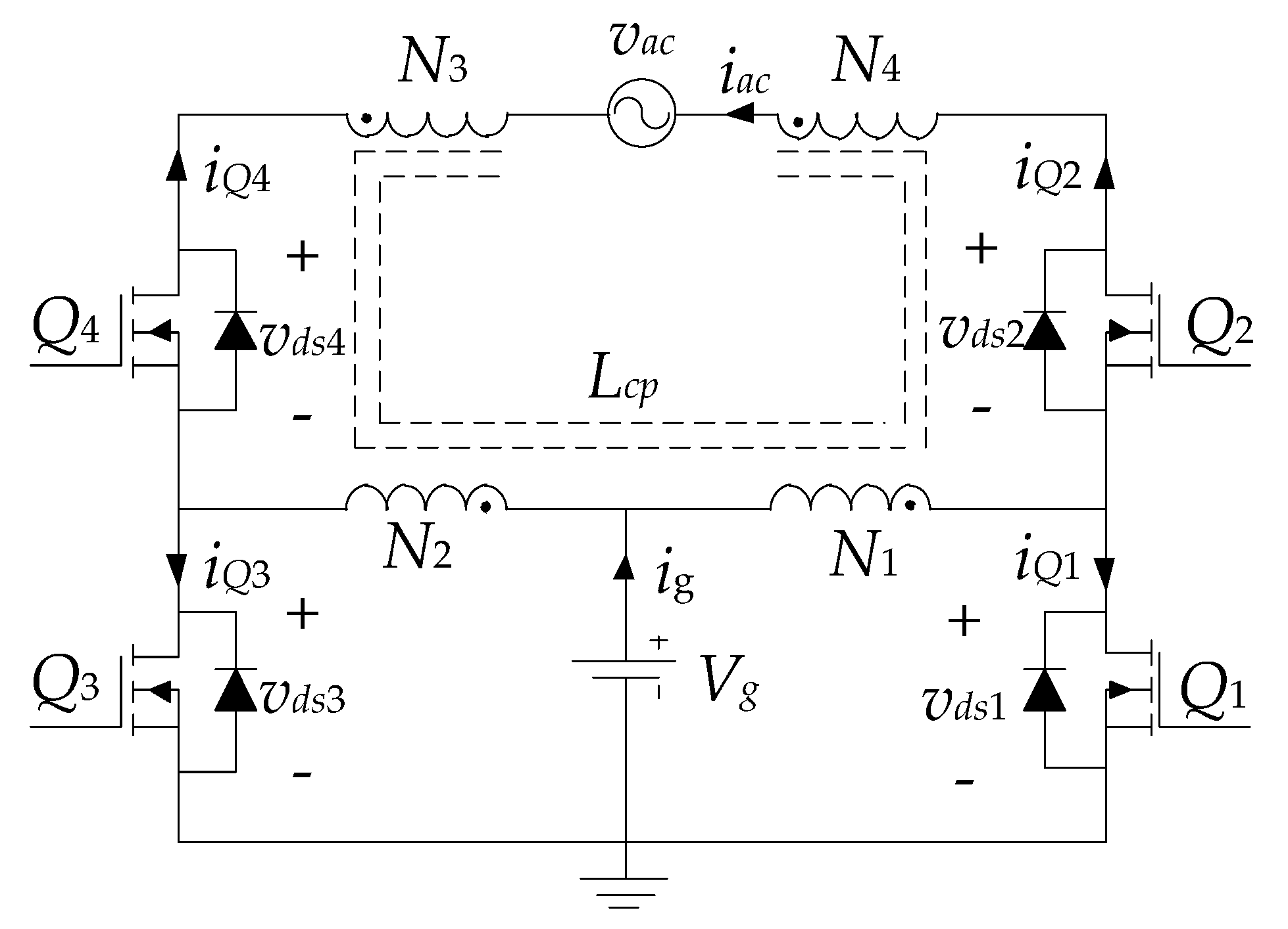
2. SSBBI Review
- Generating bipolar output current at grid level AC output voltage from a relatively low DC input voltage source without using an additional high-gain DC-DC stage;
- Low component count topology comprising a single magnetic device and four switches;
- The switches are assembled in a traditional full-bridge arrangement, suited for low-cost integrated-circuits drivers.
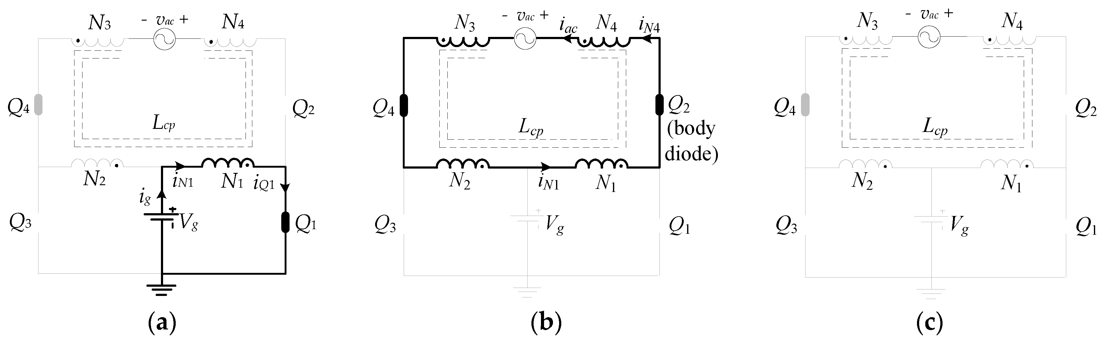
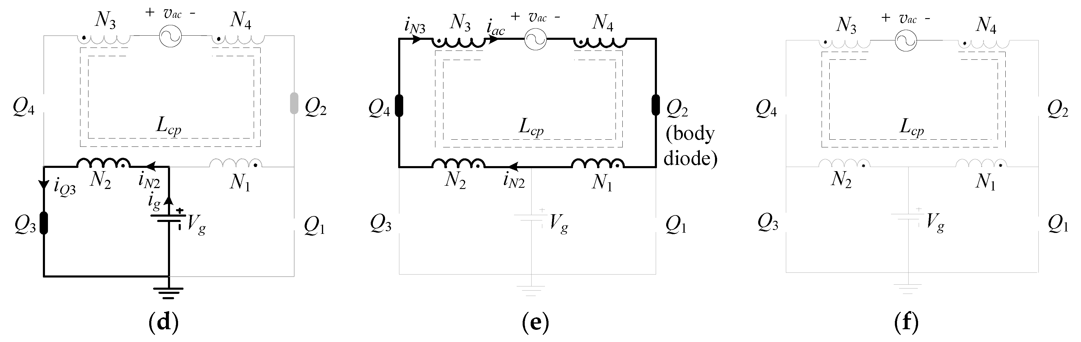
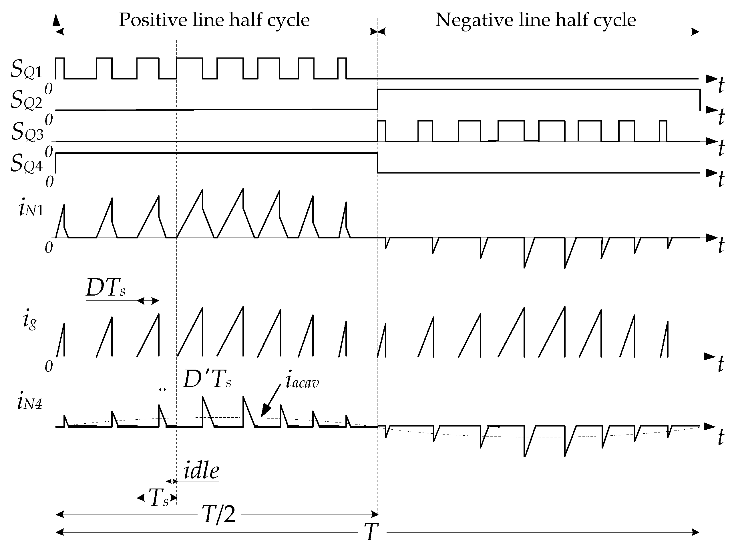
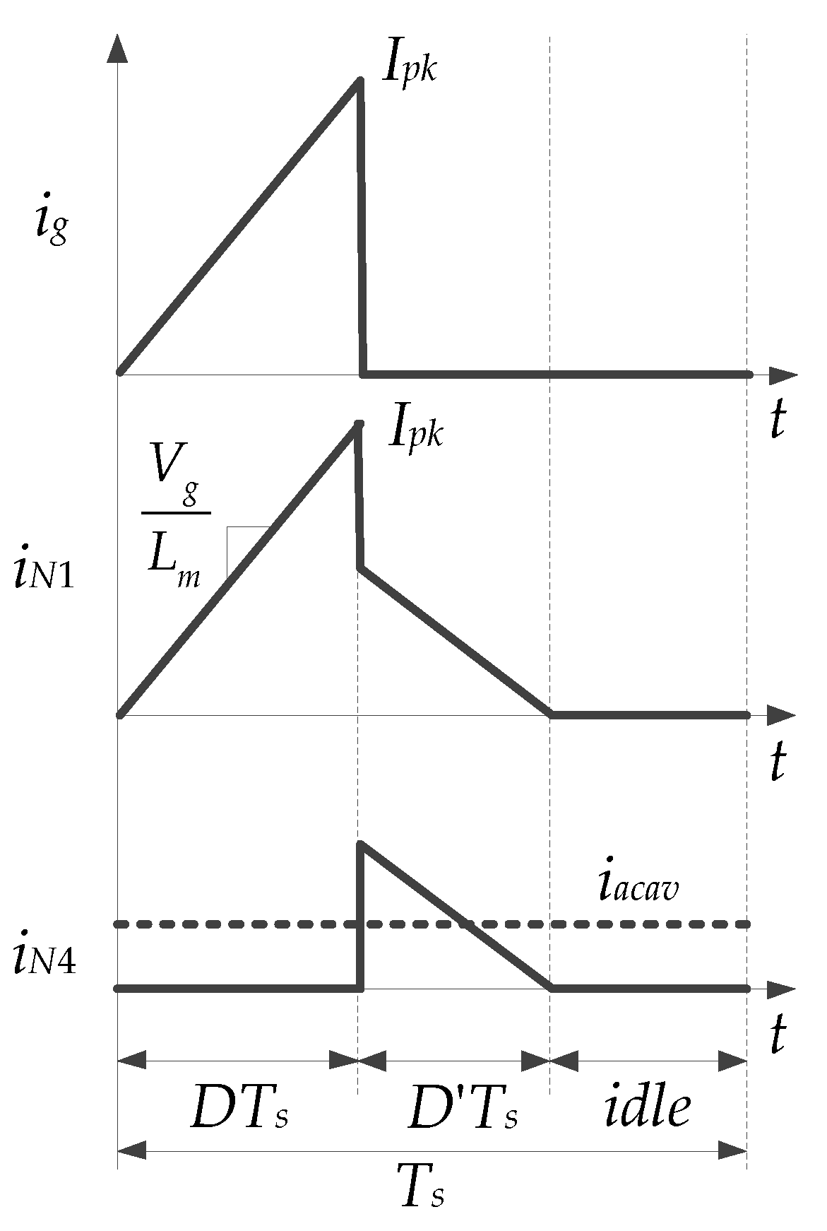
3. SSBBI Operation in the Discontinuous Conduction Mode
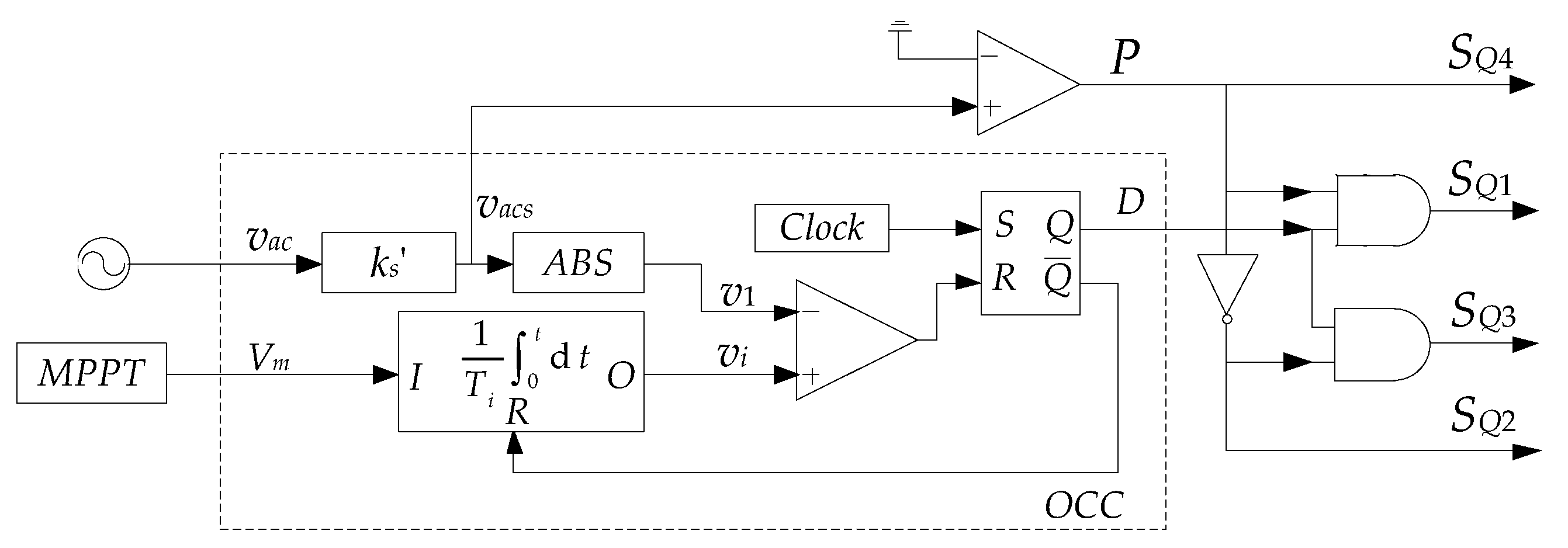
4. Derivation of OCC Control Law
5. Design Guidelines
5.1. Turn Ratio and Duty Cycle Constraints
5.2. Design Procedure
- (1)
- Choose an acceptable switching frequency, fs;
- (2)
- Choose the turn ratio, n, to satisfy Equation (13);
- (3)
- Calculate the maximum duty cycle, Dmax, according to Equation (16). Considering parameter variations and possible transients, allow the practical maximum duty cycle to assume a somewhat smaller value of Dpk = 0.85 × Dmax;
- (4)
- According to Equation (9), the average power injected into the grid is inversely proportional to the square of the modulation voltage. Thus, to generate the full rated power, PL max, the modulation voltage has to assume its minimum value, Vm min. Hence, choose an acceptable value of the modulation voltage, Vm min, that suites the dynamic range of the controller’s circuitry signal;
- (5)
- The theoretical gain of the line sensor can be derived applying the full power and the peak of the line conditions as well as using Dpk for the maximum duty cycle to Equation (6):
- (6)
- The magnetizing inductance can be obtained from Equation (9) so to satisfy the rated power requirements
- (7)
- In practice, the output voltage of the line sensor should not exceed the maximum allowed input voltage, Vin max comp, of the OCC comparator, nor can it be too small a value. To exploit the entire dynamic range of comparator’s input, the practical value of the line voltage sensor gain, ks’, can be selected according to
- (8)
- Finally, to correctly implement the OCC control law Equation (11), the integrator’s time constant is adjusted considering the ratio of the theoretically required ks, see Equation (17), and the practical ks’, set according to (19):
5.3. Design Example
- (1)
- The switching frequency of fs = 50 kHz is chosen;
- (2)
- The turn ratio according to Equation (13) is constrained by n > 0.62. Here, n = 1 is recommended;
- (3)
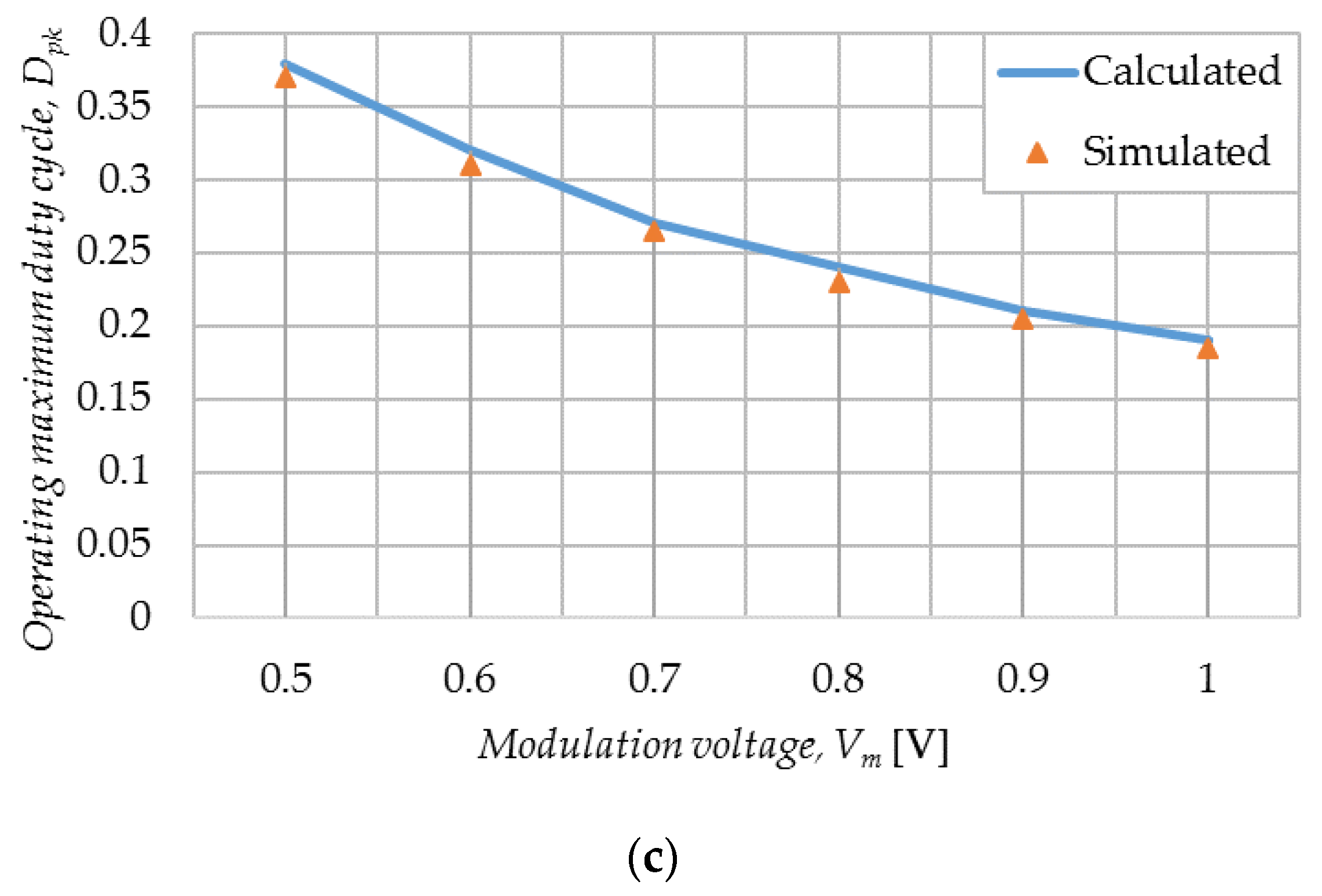
- The maximum duty cycle according to Equation (16) is Dmax = 0.447. Here, a more conservative value of Dpk = 0.38 is chosen;
- (4)
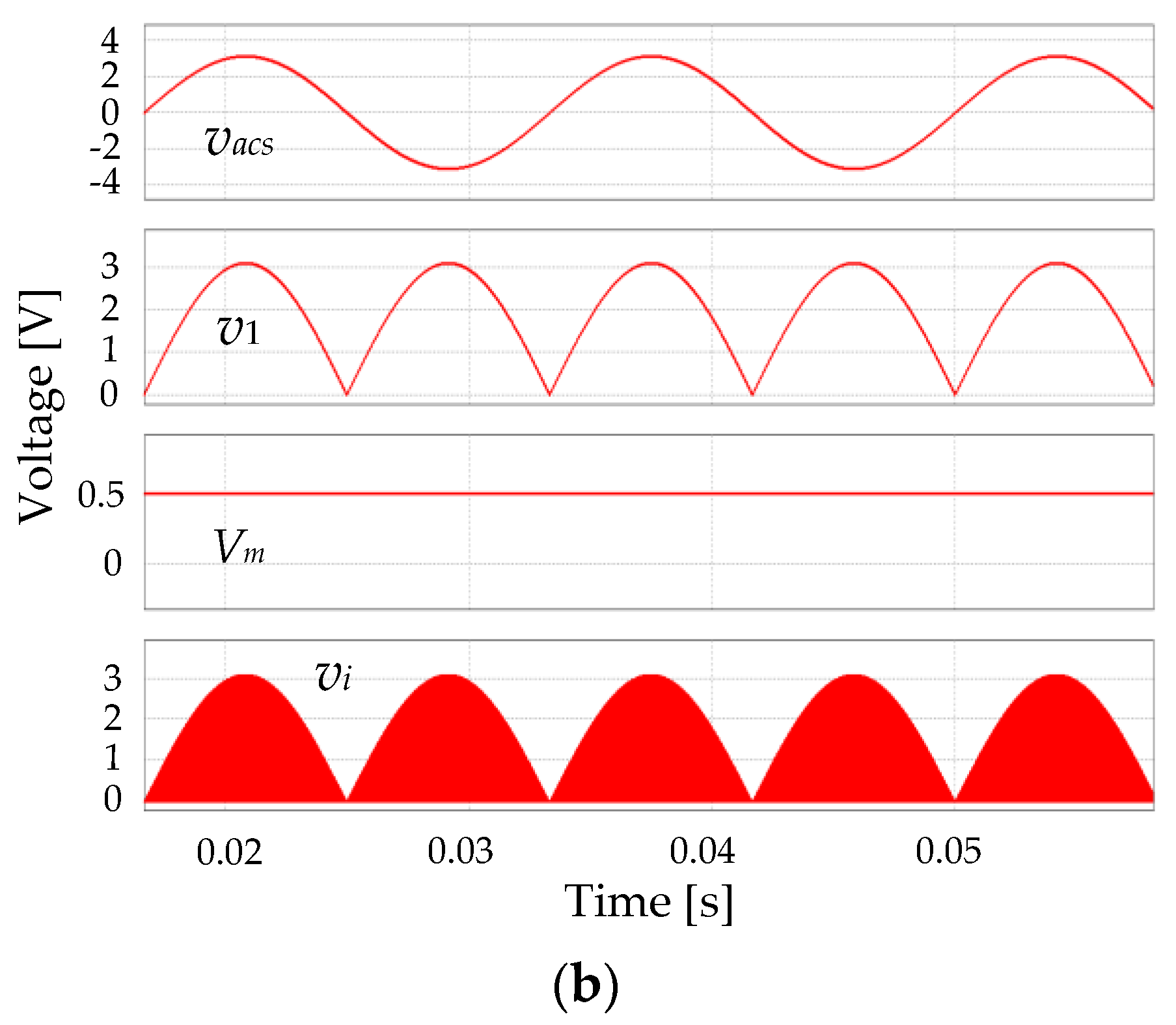
- By designer’s choice, Vm min = 0.5 at full power;
- (5)
- The required gain of the line sensor can be obtained using Equation (17) as ks = 0.0012;
- (6)
- The magnetizing inductance can be found, see Equation (18), as Lm = 16 μH;
- (7)
- By designer’s choice Vin max comp = 3 V and applying Equation (19), the practical gain of the line sensor is obtained as ks’ = 0.02;
- (8)
- Using Equation (20), the integrator’s time constant can be found as Ti = 1.2 × 10⁻⁶ s.
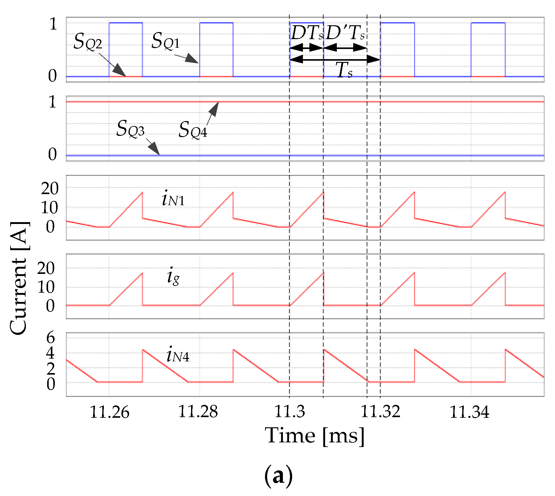
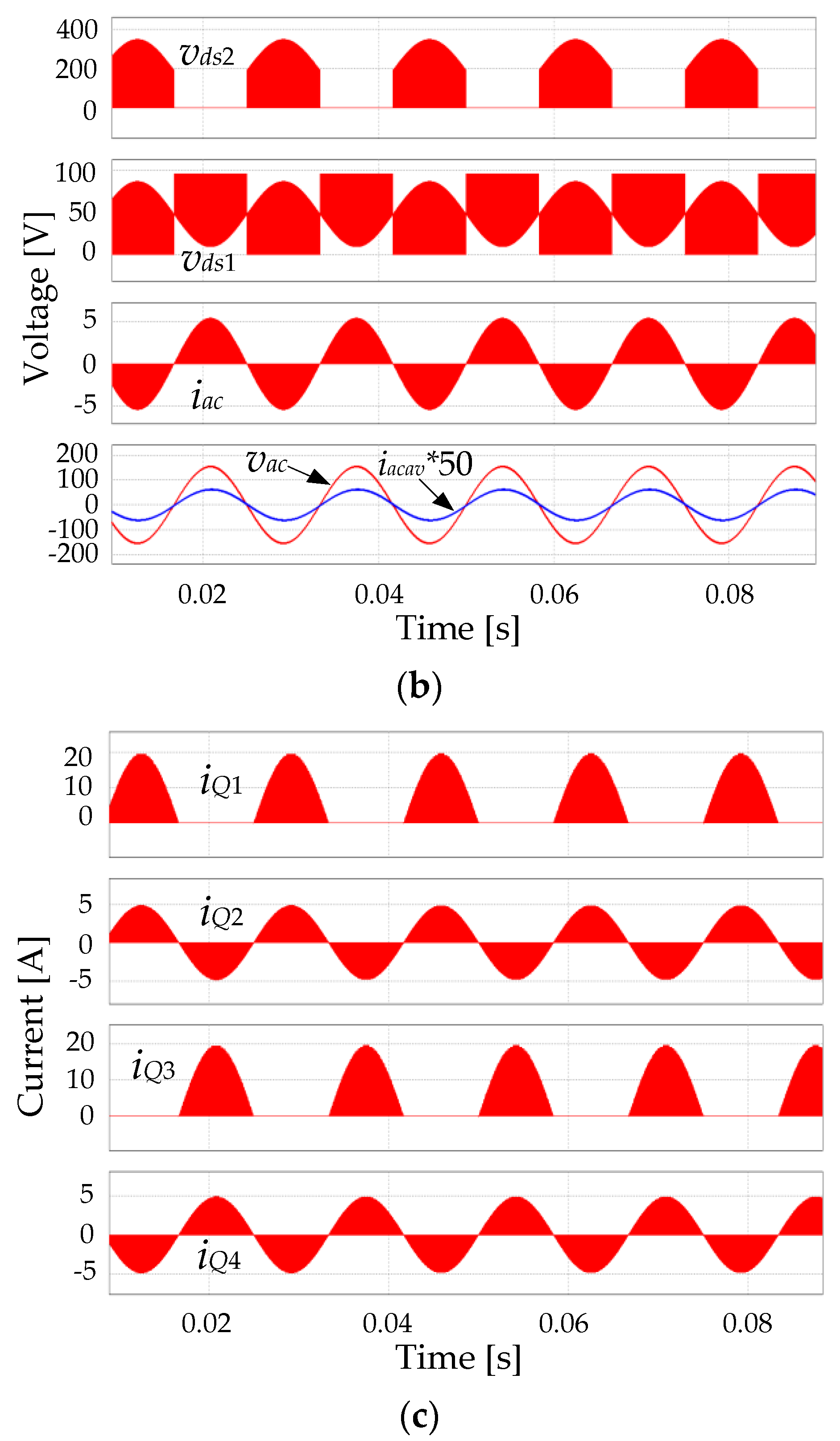
6. Simulated Results of OCC Controlled DCM GT-SSBBI
7. Conclusions
Author Contributions
Funding
Conflicts of Interest
Nomenclature and Abbreviations
| Q1, Q2, Q3, Q4, Q5 | the power switches |
| N1, N2, N3, N4 | the tapped-inductor windings |
| n | the turn ratio of the tapped-inductor |
| Co | output filter capacitor |
| vac | the AC line voltage |
| iac | the output/line current |
| iN1, iN2, iN3, iN4 | the currents through the windings |
| Vg | the input voltage |
| ig | the input current |
| iQ1, iQ3 | the currents through the switches Q1, Q3 |
| Lcp | the tapped-inductor |
| SQ1, SQ2, SQ3, SQ4 | the driving signals of the switches Q1~Q4 |
| D | the ON duty cycle |
| D’ | the OFF duty cycle |
| Ts | the switching period |
| T | the line period |
| iacav | the average output current |
| Lm | the tapped-inductor magnetizing inductance |
| Ipk | the peak inductor current |
| Epk | the peak energy stored in the magnetizing inductance |
| Pav | the average power per switching cycle |
| fs | the switching frequency |
| iacav(t) | the average current per switching cycle |
| Re | the emulated resistance of the inverter |
| Vm | the modulating voltage |
| ks | the line voltage sensor gain |
| PL | the average power delivered to the grid throughout the line cycle |
| kp | the power constant |
| Ti | the integrator’s time constant |
| Vrms | the root-mean-square value of output voltage |
| Dmax | the maximum ON duty cycle ratio |
| PL max | the inverter’s full rated power |
| Dpk | the practical maximum duty cycle |
| Vm min | the minimum value of the modulation voltage |
| Vin max comp | the maximum allowed input voltage of the OCC comparator |
| ks’ | the practical line voltage sensor gain |
| Po | the output power |
| vi | the integrator output signal of the OCC controller |
| v1 | the reference signal of the OCC controller |
| vacs | the output signal of the line voltage sensor |
| vds1, vds2 | voltage stress across the switches Q1, Q2 |
| PV | photovoltaic |
| MPPT | maximum power point tracking |
| SSBBI | single-stage buck-boost inverter |
| CCM | continuous conduction mode |
| GT-SSBBI | grid-tied single-stage buck-boost inverter |
| DCM | discontinuous conduction mode |
| OCC | one-cycle control |
| PFC | power factor corrector |
| APF | active power filters |
| GTI | grid-tied inverters |
| FC | fuel cells |
| WP | wind power |
| UPS | uninterruptable power supplies |
| DVR | dynamic voltage restorer |
| TI | tapped inductor |
| EMI | electro-magnetic interference |
| SRFF | set/reset flip flop |
References
- Rashid, K.; Safdarnejad, S.M.; Powell, K.M. Process intensification of solar thermal power using hybridization, flexible heat integration, and real-time optimization. Chem. Eng. Process.-Process. Intensif. 2019, 139, 155–171. [Google Scholar] [CrossRef] [Green Version]
- Alva, G.; Liu, L.; Huang, X.; Fang, G. Thermal energy storage materials and systems for solar energy applications. Renewable Sustainable Energy Rev. 2017, 68 pt 1, 693–706. [Google Scholar] [CrossRef]
- Meneses, D.; Blaabjerg, F.; Garcia, O.; Cobos, J.A. Review and comparison of step-up transformerless topologies for photovoltaic AC-module application. IEEE Trans. Power Electron. 2013, 28, 2649–2663. [Google Scholar] [CrossRef] [Green Version]
- Fang, Y.; Ma, X. A novel PV microinverter with coupled inductors and double-boost topology. IEEE Trans. Power Electron. 2010, 25, 3139–3147. [Google Scholar] [CrossRef]
- Abramovitz, A.; Zhao, B.; Smedley, K.M. High-gain single-stage boosting inverter for photovoltaic applications. IEEE Trans. Power Electron. 2016, 31, 3550–3558. [Google Scholar] [CrossRef]
- Kumar, A.; Gautam, V.; Sensarma, P. A SEPIC derived single-stage buck-boost inverter for photovoltaic applications. In Proceedings of the 2014 IEEE International Conference on Industrial Technology (ICIT), Busan, South Korea, 26 February–1 March 2014. [Google Scholar]
- Kumar, A.; Sensarma, P. A four-switch single-stage single-phase buck-boost inverter. IEEE Trans. Power Electron. 2017, 32, 5282–5292. [Google Scholar] [CrossRef]
- Kumar, A.; Sensarma, P. New switching strategy for single-mode operation of a single-stage buck-boost inverter. IEEE Trans. Power Electron. 2018, 33, 5927–5936. [Google Scholar] [CrossRef]
- Akbar, F.; Cha, H.; Lee, S.; Nguyen, T. A single-phase transformerless buck-boost inverter for standalone and grid-tied applications with reduced magnetic volume. In Proceedings of the 2019 10th International Conference on Power Electronics and ECCE Asia (ICPE 2019-ECCE Asia), Busan, South Korea, 27–30 May 2019. [Google Scholar]
- Zhang, Y.; Woldegiorgis, A.T.; Chang, L. Design and test of a novel buck-boost inverter with three switching devices. In Proceedings of the 2012 Twenty-Seventh Annual IEEE Applied Power Electronics Conference and Exposition (APEC), Orlando, FL, USA, 5–9 February 2012. [Google Scholar]
- Chowdhury, A.S.K.; Chakraborty, S.; Salam, K.M.A.; Razzak, M.A. Design of a single-stage grid-connected buck-boost photovoltaic inverter for residential application. In Proceedings of the 2014 Power and Energy Systems: Towards Sustainable Energy, Bangalore, India, 13–15 March 2014. [Google Scholar]
- Abdel-Rahim, O.; Orabi, M.; Ahmed, M.E. Buck-boost interleaved inverter for a grid-connected photovoltaic system. In Proceedings of the 2010 IEEE International Conference on Power and Energy, Kuala Lumpur, Malaysia, 29 November–1 December 2010. [Google Scholar]
- Tang, Y.; He, Y.; Dong, X. Active buck-boost inverter with coupled inductors. In Proceedings of the 2014 IEEE Energy Conversion Congress and Exposition (ECCE), Pittsburgh, PA, USA, 14–18 September 2014. [Google Scholar]
- Husev, O.; Matiushkin, O.; Roncero-Clemente, C.; Blaabjerg, F.; Vinnikov, D. Novel family of single-stage buck-boost inverters on the unfolding circuit. IEEE Trans. Power Electron. 2019, 34, 7662–7676. [Google Scholar] [CrossRef]
- Sreekanth, T.; Lakshminarasamma, N.; Mishra, M.K. Coupled inductor-based single-stage high gain DC-AC buck-boost inverter. IET Power Electron. 2016, 9, 1590–1599. [Google Scholar] [CrossRef]
- Sreekanth, T.; Lakshminarasamma, N.; Mishra, M.K. A single-stage grid-connected high gain buck-boost inverter with maximum power point tracking. IEEE Trans. Energy Convers. 2017, 32, 330–339. [Google Scholar] [CrossRef]
- Zhao, B.; Abramovitz, A.; Liu, C.; Yang, Y.; Huangfu, Y. A family of single-stage, buck-boost inverters for photovoltaic applications. Energies 2020, 13, 1675. [Google Scholar] [CrossRef] [Green Version]
- Smedley, K.M.; Cuk, S. One-cycle control of switching converters. In Proceedings of the PESC ’91 Record 22nd Annual IEEE Power Electronics Specialists Conference, Cambridge, MI, USA, 24–27 June 1991. [Google Scholar]
- Smedley, K.M.; Cuk, S. One-cycle control of switching converters. IEEE Trans. Power Electron. 1995, 10, 625–633. [Google Scholar] [CrossRef]
- Smedley, K.M.; Cuk, S. Dynamics of one-cycle controlled Cuk converters. IEEE Trans. Power Electron. 1995, 10, 634–639. [Google Scholar] [CrossRef] [Green Version]
- Hu, W.; Zhang, B.; Yang, R.; Qiu, D. Dynamic behaviors of constant on-time one-cycle controlled boost converter. IET Power Electron. 2018, 11, 160–167. [Google Scholar] [CrossRef]
- Zou, J.; Wang, C.; Cheng, H.; Liu, J. Triple line-voltage cascaded VIENNA converter applied as the medium-voltage AC drive. Energies 2018, 11, 1079. [Google Scholar] [CrossRef] [Green Version]
- Wang, C.; Liu, J.; Cheng, H.; Zhuang, Y.; Zhao, Z. A modified one-cycle control for Vienna rectifiers with functionality of input power factor regulation and input current distortion mitigation. Energies 2019, 12, 3375. [Google Scholar] [CrossRef] [Green Version]
- Zhang, R.; Ma, W.; Wang, L.; Hu, M.; Cao, L.; Zhou, H.; Zhang, Y. Line frequency instability of one-cycle-controlled boost power factor correction converter. Electronics 2018, 7, 203. [Google Scholar] [CrossRef] [Green Version]
- Qiao, C.; Smedley, K.M. Three-phase bipolar mode active power filters. IEEE Trans. Ind. Appl. 2002, 38, 149–158. [Google Scholar] [CrossRef]
- Wang, L.; Han, X.; Ren, C.; Yang, Y.; Wang, P. A modified one-cycle-control-based active power filter for harmonic compensation. IEEE Trans. Ind. Electron. 2014, 65, 738–748. [Google Scholar] [CrossRef]
- Yang, C.; Smedley, K.M. A cost-effective single-stage inverter with maximum power point tracking. IEEE Trans. Power Electron. 2004, 19, 1289–1294. [Google Scholar]
- Bagawade, S.; Pahlevani, M.; Pan, S.; Jain, P. Three-phase reactive power control using one-cycle controller for wind energy conversion systems. In Proceedings of the 2016 IEEE 7th International Symposium on Power Electronics for Distributed Generation Systems (PEDG), Vancouver, BC, Canada, 27–30 June 2016. [Google Scholar]


| Switches | Positive Line Voltage | Negative Line Voltage | ||||
|---|---|---|---|---|---|---|
| State A | State B | State C | State A’ | State B’ | State C’ | |
| Q1 | On | Off | Off | Off | Off | Off |
| Q2 | Off | Off | Off | On | On | On |
| Body Diode of Q2 | Off | On | Off | Off | Off | Off |
| Q3 | Off | Off | Off | On | Off | Off |
| Q4 | On | On | On | Off | Off | Off |
| Body Diode of Q4 | Off | Off | Off | Off | On | Off |
© 2020 by the authors. Licensee MDPI, Basel, Switzerland. This article is an open access article distributed under the terms and conditions of the Creative Commons Attribution (CC BY) license (http://creativecommons.org/licenses/by/4.0/).
Share and Cite
Zhao, B.; Huangfu, Y.; Abramovitz, A. Derivation of OCC Modulator for Grid-Tied Single-Stage Buck-Boost Inverter Operating in the Discontinuous Conduction Mode. Energies 2020, 13, 3168. https://doi.org/10.3390/en13123168
Zhao B, Huangfu Y, Abramovitz A. Derivation of OCC Modulator for Grid-Tied Single-Stage Buck-Boost Inverter Operating in the Discontinuous Conduction Mode. Energies. 2020; 13(12):3168. https://doi.org/10.3390/en13123168
Chicago/Turabian StyleZhao, Ben, Yigeng Huangfu, and Alexander Abramovitz. 2020. "Derivation of OCC Modulator for Grid-Tied Single-Stage Buck-Boost Inverter Operating in the Discontinuous Conduction Mode" Energies 13, no. 12: 3168. https://doi.org/10.3390/en13123168