Article

Design and Performance Evaluation of Multi-Gb/s Silicon Photonics Transmitters for High Energy Physics †

1
Dipartimento Ingegneria dell’Informazione, Università di Pisa, Via G. Caruso 16, 56122 Pisa, Italy
2
Istituto Nazionale di Fisica Nucleare, Sezione di Pisa, L. Pontecorvo 3, 56127 Pisa, Italy
3
Scuola Superiore Sant’Anna, Istituto TeCIP, Via G. Moruzzi 1, 56124 Pisa, Italy
*
Author to whom correspondence should be addressed.
This paper is an extended version of our paper published in ApplePies 2019: Applications in Electronics Pervading Industry, Environment and Society, Pisa, Italy, 11–13 September 2019; pp. 11–18.
Energies 2020, 13(14), 3569; https://doi.org/10.3390/en13143569
Submission received: 15 June 2020 / Revised: 2 July 2020 / Accepted: 8 July 2020 / Published: 10 July 2020

Abstract

:
Optical links are rapidly becoming pervasive in the readout chains of particle physics detector systems. Silicon photonics (SiPh) stands as an attractive candidate to sustain the radiation levels foreseen in the next-generation experiments, while guaranteeing, at the same time, multi-Gb/s and energy-efficient data transmission. Integrated electronic drivers are needed to enable SiPh modulators’ deployment in compact on-detector front-end modules. A current-mode logic-based driver harnessing a pseudo-differential output stage is proposed in this work to drive different types of SiPh devices by means of the same circuit topology. The proposed driver, realized in a 65 nm bulk technology and already tested to behave properly up to an 8 MGy total ionizing dose, is hybridly integrated in this work with a lumped-element Mach–Zehnder modulator (MZM) and a ring modulator (RM), both fabricated in a 130 nm silicon-on-insulator (SOI) process. Bit-error-rate (BER) performances confirm the applicability of the selected architecture to either differential and single-ended loads. A 5 Gb/s data rate, in line with the current high energy physics requirements, is achieved in the RM case, while a packaging-related performance degradation is captured in the MZM-based system, confirming the importance of interconnection modeling.

1. Introduction

Multi-Gb/s serial data links are largely deployed in high energy physics (HEP) environments to exchange data between on-detector readout modules and off-site processing electronics. Luminosity and sensors’ granularity growth foreseen for future HEP experiments will lead to a tremendous increase in data volumes and radiation exposures [1]. State-of-the-art radiation-tolerant optical links have been developed in the framework of versatile link (VL) and gigabit transceiver (GBT) projects and are now deployed inside the Large Hadron Collider (LHC) experiments at CERN [2,3]. They are currently based on both single-mode edge-emitting lasers (EELs) and multi-mode vertical cavity surface emitting lasers (VCSELs) [4], which are directly modulated by means of radiation-hard application-specific integrated circuits (ASICs) [5]. Laser diode-based technologies however suffer from radiation-induced degradation caused by displacement damage. In the next-generation HEP apparatus, particle fluences will become too high ( 10 16 c m 2 1 MeV neutron equivalent) to guarantee VCSELs’ operation in the innermost detector layers, and suitable alternatives need to be investigated [6].
In the last few decades, silicon photonics (SiPh) has attracted interest as a viable technology for the realization of power-efficient short-reach optical interconnects. The low-cost, high-yield, and complementary metal oxide semiconductor (CMOS) fabrication processes along with the possibility to integrate different optical functionalities on a single chip allowed it to rapidly become the workhorse of datacom businesses [7]. A similar traction is gradually rising also inside the HEP community since silicon (Si) has already been proven to be an excellent radiation-tolerant material [8]. Moreover, the technological compatibility with electronics opens up new levels of integration at the detector-level, which can alleviate material budget constraints [9].
Much effort has been focused on verifying whether SiPh-based data links can tolerate the harsh conditions typical of HEP experiments. SiPh devices are relatively insensitive to neutron radiation, but they show strong degradation under ionizing X-rays exposure [10]. It was proven that the X-ray-induced impairments can be moved beyond the MGy-level by following some radiation-hardening-by-design (RHBD) techniques [11] or by periodically modifying the driving conditions [12].
Given the recent technology readiness level (TRL) boost, SiPh modulators are starting to become almost as commercial off-the-shelf (COTS) components [13]. Many foundries already provide design kits and layout cells of photonic components that ever more frequently lead to modulation performances up to 50 Gb/s [14]. Nevertheless, equally high-speed and radiation-resistant ASICs are needed to interface these photonic devices with the front-end electronics and make the complete readout units fit into compact modules. From a system-level viewpoint, the best achievement would be the realization of an electronic circuit that is capable of driving a broad variety of SiPh devices, mimicking the GBT driving flexibility for the laser diode case [15]. SiPh-based wavelength division multiplexing (WDM) schemes applied to HEP scenarios are currently under development, and the exploitation of general-purpose drivers could indeed help to attain high aggregate bandwidth readout systems [16].
In this work, we will show that small architectural changes to conventional CMOS drivers for SiPh devices can enable multi-Gb/s transmission on both lumped-element Mach–Zehnder modulators (MZMs) and ring modulators (RMs), at least for relatively low bandwidths compared to datacom frameworks, but still of interest for HEP applications. This paper extends the contribution in [17] in terms of conceptual modeling and experimental results, evaluating the operation of a full-custom CMOS driver with different classes of SiPh modulators.
Section 2 provides a background on SiPh modulators and traditional driver circuits. Section 3 discusses the proposed driver topology and describes the circuital choices that make it appropriate both for MZMs, as well as RMs. Finally, experimental procedures and system-level characterization results are respectively presented in Section 4 and Section 5. Conclusions and further perspectives are drawn in Section 6.

2. Background

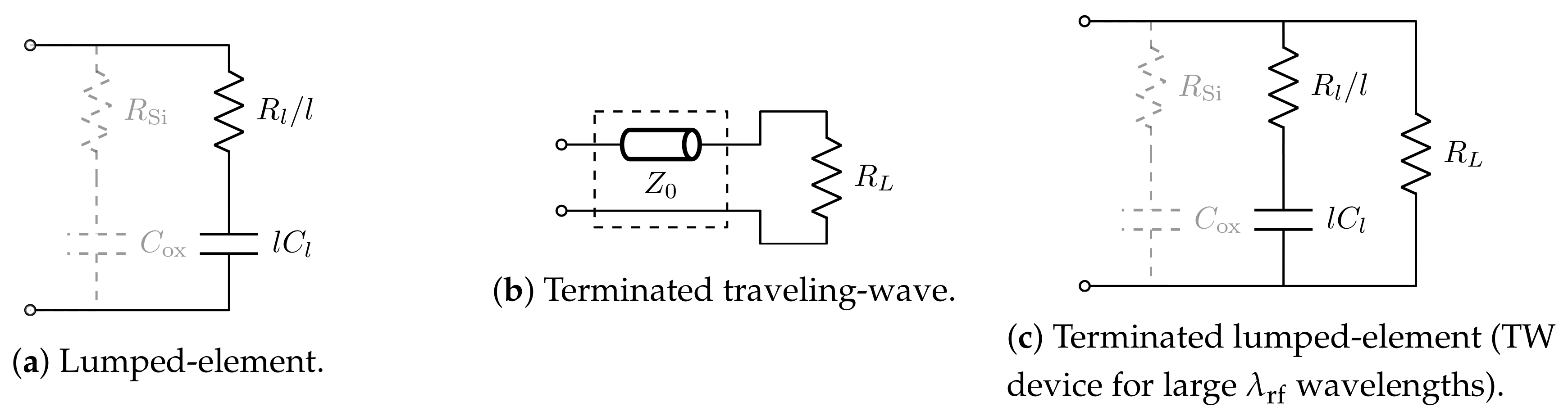
2.1. Silicon Photonics Modulators

In SiPh technologies, an optical modulator is usually realized by embedding a pn-junction inside a waveguide [18]. It is well known that the presence of free charge carriers, i.e., electrons and holes, can change the refractive index of a semiconductor material [19]. By varying the pn-junction bias voltage, free-carriers’ distributions change across the waveguide, and the phase velocity of the propagating optical mode is modified. Depletion-mode operation ensures high-speed phase modulation since only majority-carriers’ dynamics are involved [20]. Amplitude modulation can be achieved by inserting phase shifters into interferometric, e.g., MZMs [21], or resonant architectures, e.g., RMs [22,23]. Information is indeed typically encoded in the light intensity, and the simple on-off keying (OOK) is one of the most adopted modulation formats, although more complex schemes are emerging, e.g., PAM-4 [24].
In order to make efficient designs for the electronic driver, it is important to carry out an electrical equivalent circuit of the phase shifter under study. The reverse-biased diode can be represented by a voltage-dependent junction capacitance in series with the access resistances associated to the ohmic conduction through the anode and cathode doped slabs. The junction capacitance per phase shifter length C l is typically around hundreds of fF/mm, while the per-unit-length resistance R l is normally about a few Ω · mm. For modulation wavelengths λ r f , which are greatly larger than the device dimensions, i.e., l λ r f , the appropriate circuit model for a phase shifter of length l is depicted in Figure 1a. In the limits of this approximation, the overall device behavior is captured by means of lumped-elements (LEs), and the intrinsic (−3 dB) bandwidth results [20]:
f 3 d B = 1 2 π R l C l + Z d r v l C l
Assuming a purely real driver output impedance Z d r v and neglecting all the parasitic contributions. Being proportional to the amount of charge carriers that are swept in and out the active device region, C l is directly related to the phase shifting efficiency, which is commonly quantified by the V π l figure of merit. Since the free-carrier effects are weak in silicon, V π l typically ranges between 10 V · mm and even 40 V · mm depending on the implant conditions [26]. Because the available voltage span is typically no more than a few volts in deep sub-μm CMOS technologies, phase shifters are normally operated with voltage swings substantially lower than the rated V π [27]. Interference-based modulators are then made a few millimeters long to accumulate enough phase shift and provide reasonable optical extinction ratios (ERs). As a consequence, the total capacitance l C l is enlarged, and f 3 d B is diminished according to Equation (1). On the other hand, compact devices, such as RMs, present small lumped capacitances and can guarantee high cutoff frequencies from a purely electrical point of view, i.e., ignoring photon lifetime-related effects.
To cope with the capacitance-limited response of long modulators, traveling-wave (TW) devices are usually conceived. By designing phase shifters as transmission lines (TLs), the capacitive loading could be accurately “mixed up” with the inductive contribution of the coplanar electrodes, and the whole device, when properly terminated, globally appears as a (resistive) load equal to the TL’s characteristic impedance Z 0 (Figure 1b). By choosing R L Z 0 Z d r v , impedance matching can be theoretically achieved (neglecting parasitics), and by making them equal to 50 Ω, the compatibility with common testing instrumentation can be maintained. However, the TW behavior manifests only at frequencies for which the LE approximation no longer holds. Otherwise, for relatively low modulation frequencies, a TW modulator appears as an LE device in parallel with the termination impedance R L , as sketched in Figure 1c.

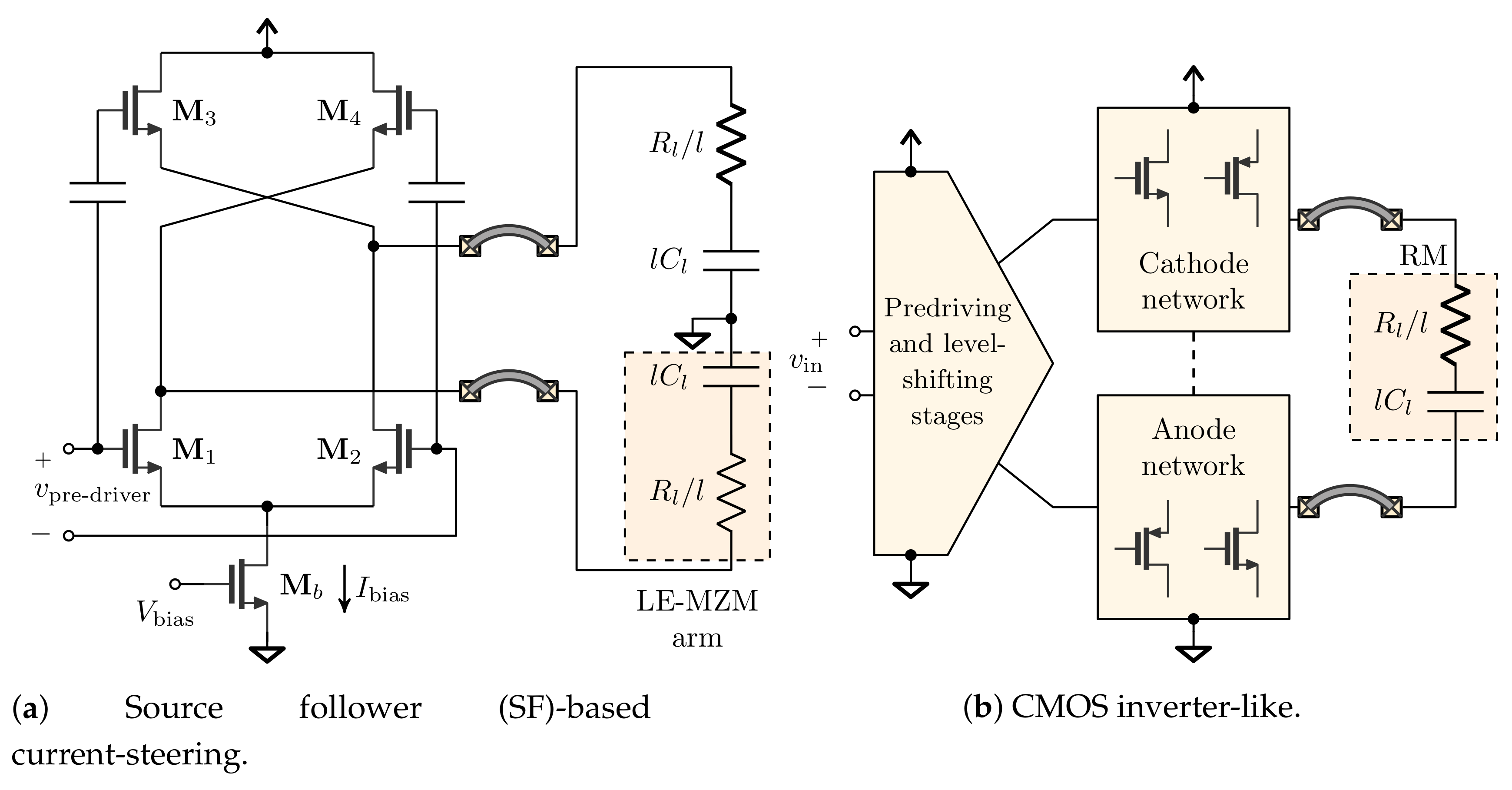
2.2. Driving Architectures

Depending on the SiPh modulator to be driven, some circuit architectures are more suitable than others, in particular regarding the output stage. As a general frame of reference, differential loads are usually driven by current mode logic (CML)-inspired architectures, while single-ended (SE) devices are traditionally actuated with CMOS inverter-like stages. The latter indeed consume less static power, but are characterized by lower speed ratings compared to their current-steering counterparts [26]. Moreover, TW loads need to be as closely impedance-matched as possible with the conditioning electronics to avoid signal reflections, while LE modulators require low driving impedances ( Z d r v ) to extend the operational bandwidth, according to Equation (1).
MZMs have a differential structure that is always actuated in push-pull (PP), i.e., by applying opposite signals to the phase shifters in the interferometer arms. Standard common-source (CS) differential pairs are generally implemented to realize PP driving. Figure 2 reports two widely exploited topologies for TW-MZMs [28]. In the “open-drain” version, all the available current flows in the modulator without undergoing partitionings, so the maximum available voltage swing develops on the termination resistors. This notwithstanding, the high output impedance provided by the drain connections makes this architecture vulnerable to impedance discontinuities. Both near-end and far-end reflections are usually dealt with using a “double-termination” structure [29], which resembles a standard CML buffer where the biasing load branches are impedance-matched to the SiPh TW load. However, in this case, the modulator is fed with a lower voltage swing compared to the “open-drain” version, in the same power consumption conditions. The internal termination is indeed connected in parallel to the SiPh modulator, thus lowering the effective load impedance.
Differential LE modulators, e.g., sections of segmented MZMs, can also be actuated by current-steering stages. As sketched in Figure 3a, source follower (SF) output stages can be used in this case to present a low output impedance [30]. On the other hand, drivers for single-ended LE phase shifters are traditionally designed by stacking several transistors on top of each other in a CMOS configuration to extend the output voltage swing, as shown in Figure 3b. Floating supply rails, together with level shifter circuits, are then harnessed to meet technological reliability requirements [31]. In the specific case of RMs, two different output stages are sometimes used to drive the modulator terminals independently [32]. In this way, a little forward bias can be introduced into the driving waveform to enlarge the optical ER.

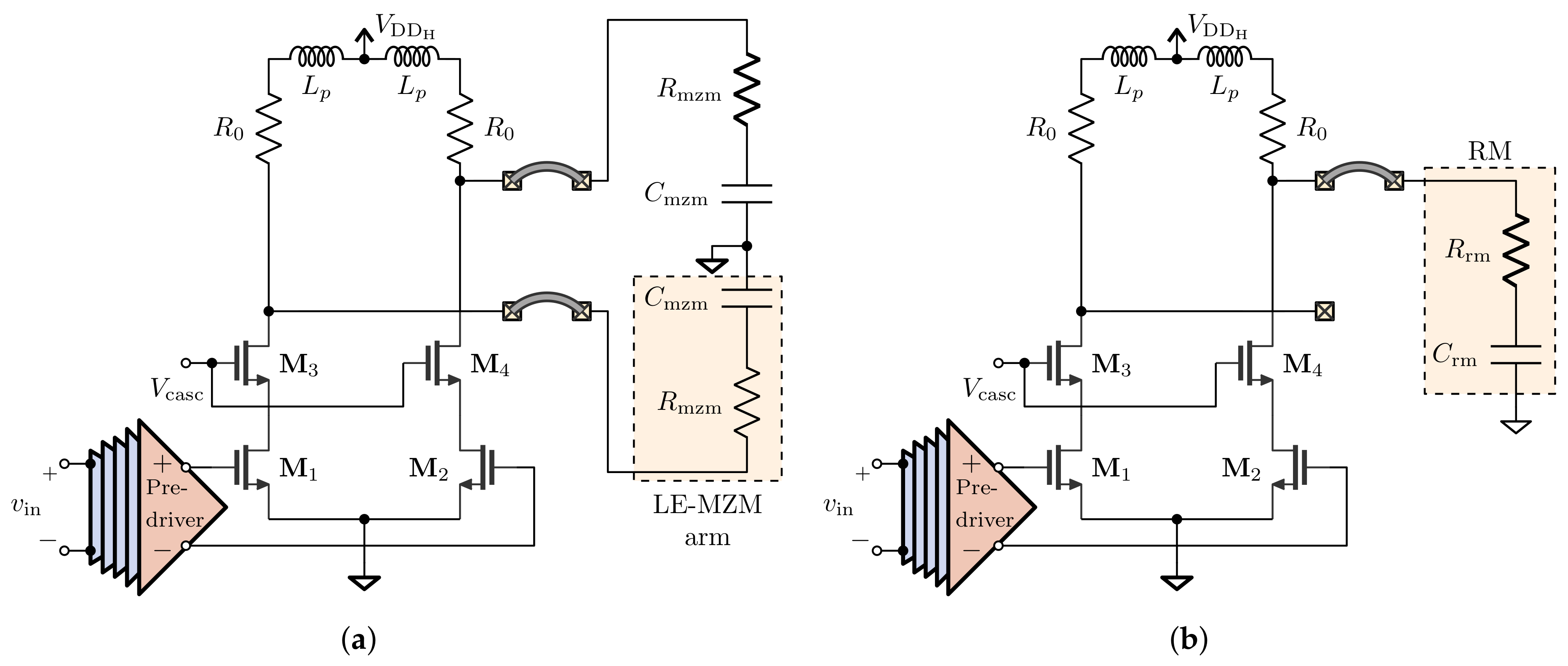
3. Proposed Driver Design

Radiation tolerance requirements pose severe limitations in the design of an ASIC. Recently, several studies were conducted on deep sub-μm platforms suitable for high-speed applications, e.g., 65 nm [36] and, even more recently, 28 nm [37] technologies. Total ionizing dose (TID)-induced charge trapping determines transistor parameter drifts and leads to the formation of current leakage paths in active regions next to shallow trench isolations (STIs) [38]. Moreover, p-type MOSFETs result in being less tolerant than n-type ones, and radiation-induced short/narrow channel effects are reported. As a consequence, few RHBD techniques have been drawn to extend the radiation hardness of a given ASIC design [39]. According to those rules, p-type and minimum-length MOSFETs have not been used throughout the design, and only thin-oxide enclose layout transistors (ELTs) have been exploited [40].
The whole driver consists of a five stage tapered chain of standard CML buffers followed by the proposed output stage, which needs to be capable of driving both differential, as well as single-ended SiPh modulators. The aforementioned radiation-related guidelines affect the architecture choice for the last stage. CMOS-like solution are surely not feasible since they harness p-MOSFETs. However, current steering structures, such as those presented in Section 2.2, are also not suitable. Connecting an LE phase shifter directly to the two output leads, the differential swinging would determine the pn-junction forward biasing. Instead, loading only one branch with a single-ended load would unbalance the circuit. Dummy loads can in principle be used to restore the balance, as is sometimes done in certain drivers [41]. Nevertheless, they undoubtedly introduce mismatches and possibly lead to spurious phase modulation at GHz-range frequencies, affecting jitter performances [29].
As shown in Figure 4, a pseudo-differential structure, i.e., a differential pair without a tail current source, appears to be a viable solution for the problem. Resistive pull-up is preferred to the SF-based topologies to save the voltage drop on the upper transistors and get the highest possible swing out of the circuit. Conventional SF-based topologies do not produce voltage gain, and their usage leads to more complex pre-driving and output stage designs [42]. For the ease of testing and to drive also terminated devices, the internal load resistors, indicated with R 0 in Figure 4, are nominally chosen as 50 Ω. The tail current source removal also helps in enlarging the peak-to-peak output swing by saving the voltage headroom normally left for the biasing MOSFET (on the order of an overdrive voltage). The common-mode level of the last pre-driving CML stage should be lowered approximately by the same amount in order to drive the input transistors of the output stage properly. Anyway, the intrinsic input common-mode sensitivity associated with pseudo-differential structures has no great importance in this specific case since, dealing with non-return-to-zero (NRZ) signals, the circuit operates in switching large-signal mode [29]. To further increase the output swing, a doubled supply voltage V D D H = 2.4 V (with respect to the 1.2 V applied elsewhere) is used in the last stage. A cascode structure is then implemented to keep voltage stresses on MOSFETs in the technology’s safe operating area (SOA). Harnessing thick-oxide devices in the series transistor stacking could have allowed increasing even more the output supply voltage. However, radiation-hardening constraints prevented their exploitation for circuits targeted to sustain MGy-range TIDs.
Inductive peaking was also introduced in the last two stages to extend the bandwidth [43]. Inductors ( L p ) have been realized with a differential layout with a central tap to save area. Further details about the circuit design and purely electrical measurement results can be found in [44].

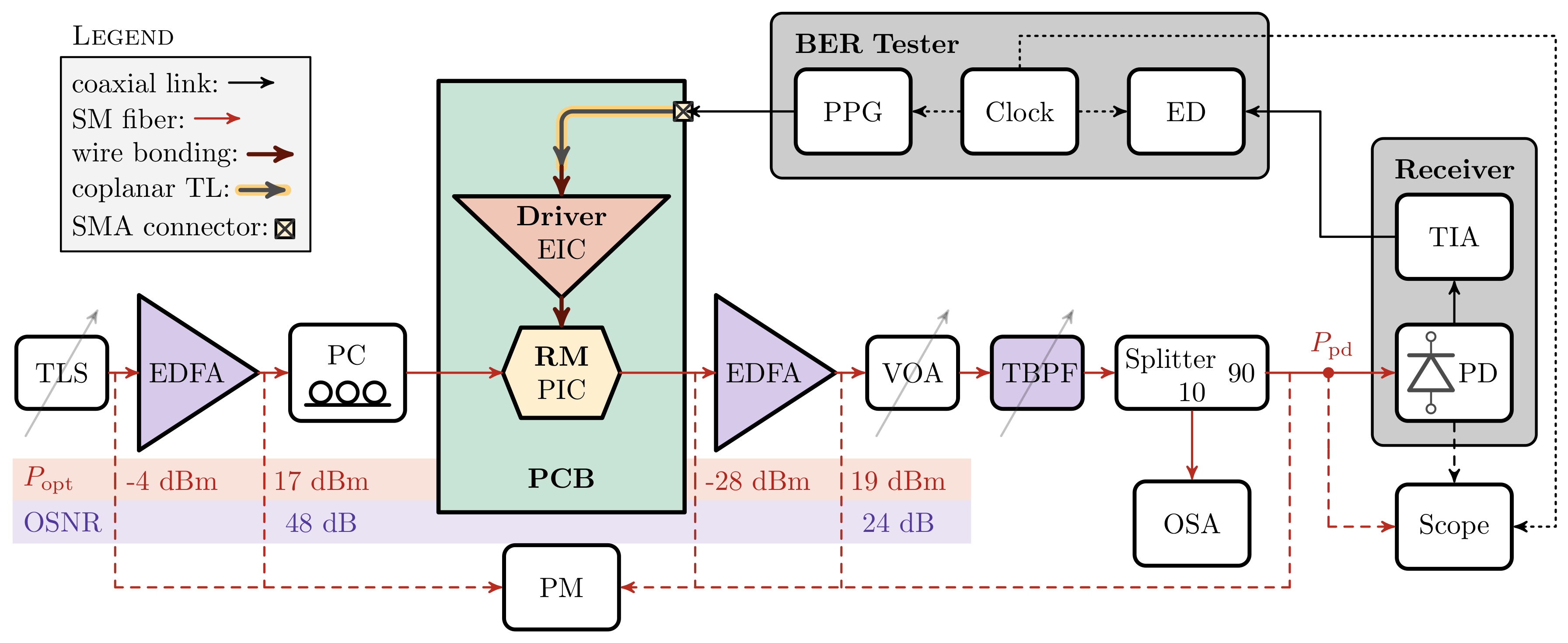
4. Experimental Setup
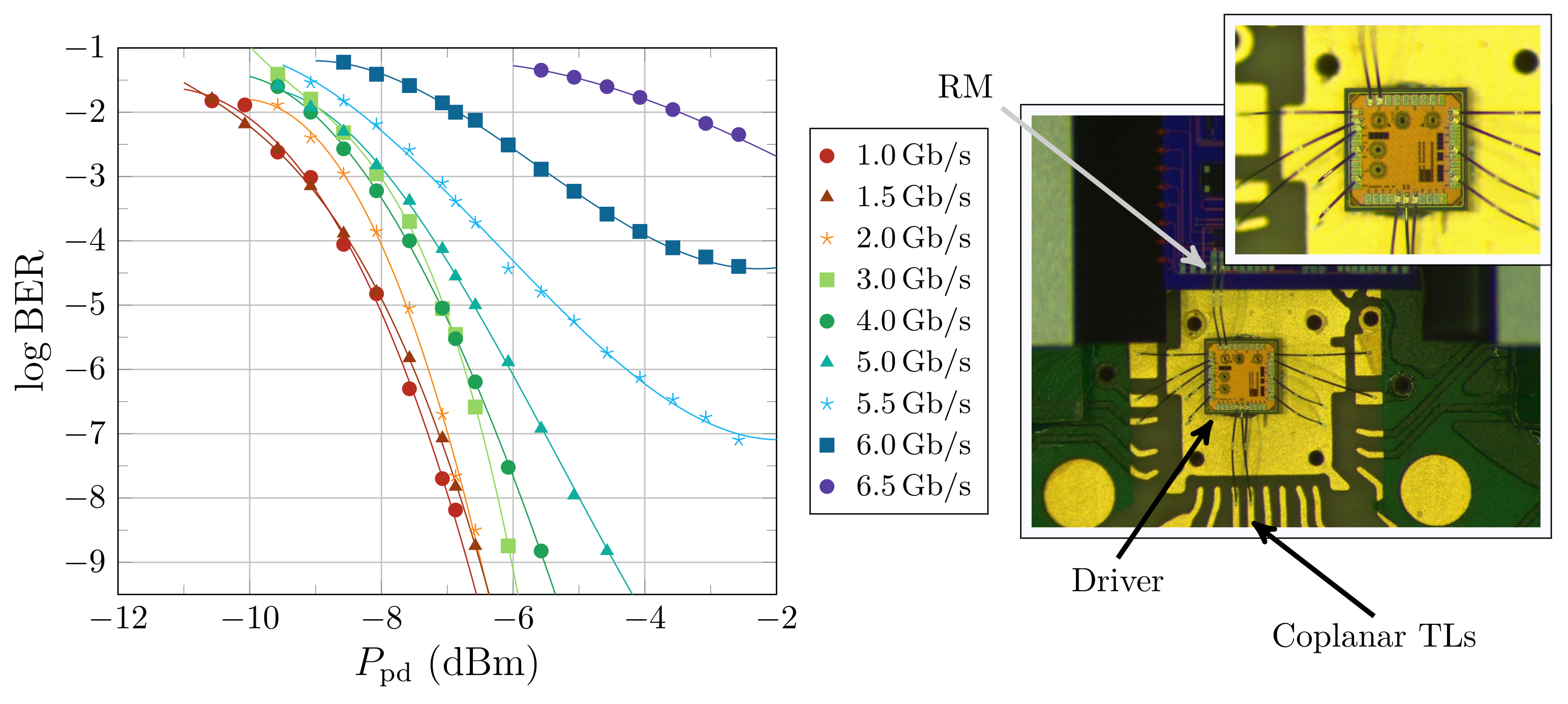
4.1. Samples

The proposed driver was included in a 1   m m × 1   m m electronic integrated circuit (EIC) fabricated in a commercial-grade radiation-hard 65 nm CMOS technology. The circuit radiation resistance was previously tested exposing the whole EIC to X-rays at the INFN-Padova facility. Proper operation of the standalone driver was observed till a total ionizing dose (TID) of 8 MGy, which was the highest dose level reached during the test because of limited testing time. A 30% voltage amplitude degradation with respect to the pre-irradiation value was observed [17]. In addition, a single event upset (SEU) analysis of the same circuit was carried out in [44], proving its HEP-level radiation-tolerance.
In this work, the proposed driver was tested together with two SiPh optical modulators fabricated in a SiPh 130 nm silicon-on-insulator (SOI) process, i.e., an MZM and an RM. They were based on the corresponding building blocks provided in the foundry’s process design kit (PDK) and were laid out in a 5   m m × 5   m m photonic integrated circuit (PIC) [45]. They both relied on 450   n m × 220   n m rib-waveguide phase shifters with deep-etched slabs and used standard doping levels.
The MZM was 1 mm long and was drawn with unbalanced arms, i.e., one arm was physically made longer, which allowed tuning the operating point by changing the laser wavelength. Each arm was sized as a coplanar waveguide (CPW), and the electrodes’ layout matched the output port pattern of the full-custom driver. Although having been designed as a TW device, each MZM arm lacked an on-chip termination and effectively behaved as a lumped-element for the frequencies of interest. The associated pn-junction capacitance C m z m was estimated to be around 0.5 pF. Wafer-level radio-frequency (RF) measurements made on comparable MZM designs ensured that the electro-optical modulation bandwidth was above 10 GHz with a proper termination [14].
The ring modulator had a 7.5 μm radius resulting in a free spectral range (FSR) of about 13 nm. As shown in Figure 5, the resonance next to 1.55 μm had a full-width at half-maximum (FWHM) of about 240 pm and an extinction depth of nearly 20 dB. The spectrum was measured by feeding the device with a tunable external cavity laser (ECL) and sweeping the wavelength in the 1510 nm to 1570 nm range with a 0.82 pm resolution. The LE capacitance C r m associated with the RM was expected to be on the order of a few tens of femtofarads. Electronic and photonic dies were placed on a printed circuit board (PCB) and bonded with 40 μm diameter aluminum (Al) bond-wires. Tapered coplanar transmission lines were realized on the PCB to maintain the 50 Ω impedance environment while transitioning from the centimeter-scale footprint of the high-speed SMA (SubMiniature, Version A) connectors to the 100 μm bond-pads’ pitch. A PCB with the same layout was used for both characterizations. The complete packaged sample is shown in Figure 6.
Fiber-to-PIC light coupling was achieved by means of on-chip grating couplers and quasi-planar fiber-arrays. The latter were preferred to the vertical fiber couplers because of their lower encumbrance on the PIC surface [46]. Fiber arrays were manually pigtailed with the aid of micro-mechanical stages and active alignment tools. An index-matched epoxy cured with ultra-violet (UV) light was used to bond the silica fiber holder to the PIC in the position that gave the best insertion loss. Given the μm-scale positioning tolerance of the grating-based coupling, the fiber-array ribbons were also glued on the PCB to limit the mechanical stresses on the fiber holder during manual handling (see Figure 6).

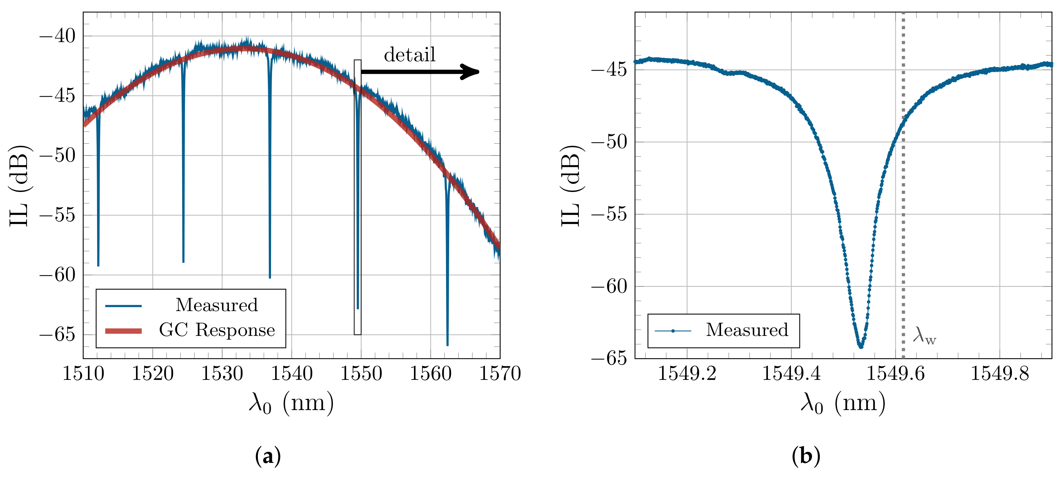
4.2. Measurement Procedures

A standard on-off keying (OOK) optical link was set up to characterize the SiPh-based transmitter with the devices under test. In order to quantify the transmission reliability, the bit error rate (BER) was chosen as a reference parameter. Optical links that were employed in HEP experiments covered at most distances on the order of hundreds of meters and, in principle, did not need to be optically amplified. To mimic the final application scenario, BER performances were evaluated at a constant optical signal-to-noise ratio (OSNR) by varying the optical power at the receiver [47].
Two different electronic dies were used for each SiPh modulator characterization. The measurements were made in distinct time slots; hence, the working conditions were not exactly the same for both cases. Figure 7 and Figure 8 depict the experimental setups respectively built up for the MZM and the RM characterizations. Some elements were common to both scenarios. A 12.5 Gb/s BER tester (BERT) stimulated the device under test (DUT) and calculated the BER. A pulse pattern generator (PPG) encoded a pseudo-random bit sequence (PRBS) on an NRZ electrical signal with voltage levels suitable to feed the input CML stage of the driver, i.e., a symmetric 400 mV voltage swing with 1 V DC bias. A PRBS pattern 2 31 1 -long was chosen in order to make a repetitive measure with the largest number of bit combinations. The out-coupled modulated optical power was converted back in the electrical domain by means of a commercial 10 GHz-bandwidth module comprising a photo-detector (PD) and trans-impedance amplifier (TIA). An error detector (ED) compared the transmitter and received bit sequences and detected transmission errors. The two bit streams were synchronized by physically sharing the clock between PPG and ED. The voltage decision threshold and the sampling time on the ED were adjusted to get the lowest BER.
Optical power was provided by a tunable light source (TLS) near 1.55 μm. It was adjusted in order to operate the MZM in quadrature and the RM around the wavelength λ w shown in Figure 5, which was verified to generate the largest eye opening given the actual voltage swing delivered by the driver. Since grating couplers were only sensitive to transverse-electric (TE) fields, a polarization controller (PC) was placed upstream the DUT to maximize the coupled power. In the RM characterization, a 90/10 splitter was inserted before the PD in order to continuously monitor the output signal spectrum with an optical spectrum analyzer (OSA). This allowed measuring the OSNR at the receiver and detecting eventual working point shifts during measurements. Eye diagrams were captured by connecting the PD to a 40 GHz-bandwidth oscilloscope (the BERT clock signal was used to trigger the waveform acquisition).
Both boards under test showed huge optical insertion losses (ILs), roughly 20 dB fiber-to-fiber IL for the MZM test chip and 40 dB in the RM case, as can be seen from Figure 5a. They were mainly attributed to accidental misalignments between the fiber array holder and the on-chip grating coupler array, probably occurred during the boards’ shipping. Fiber-to-fiber ILs after the fiber array attachment were indeed measured to be around 12 dB in both cases. For this reason, some erbium-doped fiber amplifiers (EDFAs) were added to the optical signal chains. Two EDFAs were used for the RM testing because of the more severe optical losses in that specific case. A 0.3 nm tunable band-pass filter (TBPF) was also inserted in both setups to suppress the ASE-ASE (amplified spontaneous emission) beat noise in the photo-detection. These additional elements are highlighted in violet in Figure 7 and Figure 8. EDFA gains and laser powers were tuned in order to have large OSNR values at the receiver and enable a system-level characterization even in the presence of this IL impairment. Large OSNR levels were necessary to attribute any transmission penalty to the transmitter functionality.

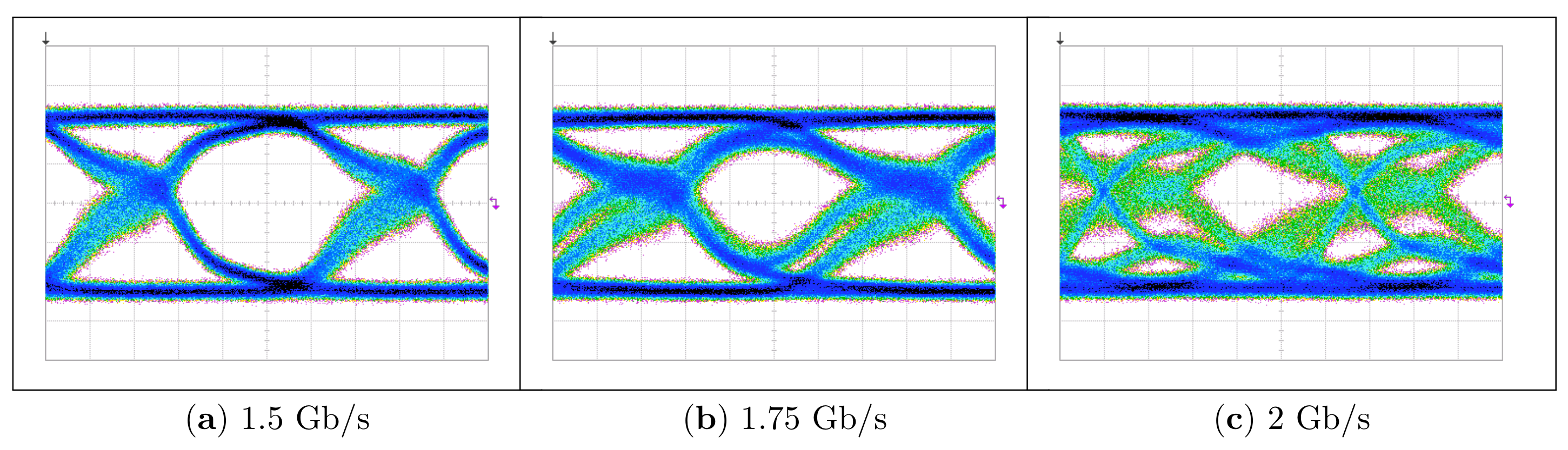
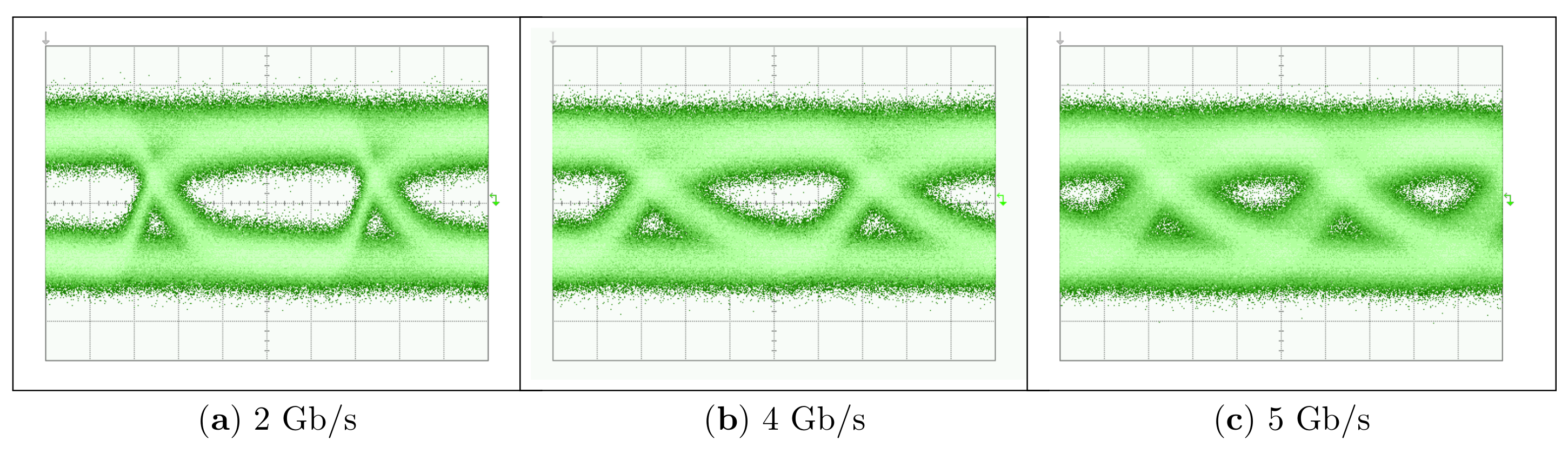
5. Results and Discussion

Measured BERs as a function of the input power P p d on the photo-detector are shown for different data rates in Figure 9 for the MZM testing case. The whole system worked up to a bit-rate of 1.5 Gb/s, while BER floors started to appear around 1.7 Gb/s, and a completely compromised transmission functionality was captured already at 2 Gb/s, as shown in Figure 10.
The results for the RM-based system are instead shown in Figure 11 and Figure 12. BER floors here became visible only above 5.5 Gb/s, and data transmission at 5 Gb/s with BER below 10 9 was confirmed to be achievable with optical power levels on the receiver side ( P p d ) greater than −4 dBm. The eye diagrams in Figure 11 were all taken in the condition P p d = 6 dBm to be comparable. In that situation, the cases corresponding to the 4 Gb/s and 5 Gb/s data rates did not represent error-free scenarios, as confirmed by the BER plot, and their apparent narrow eye aperture was therefore justified. Moreover, in line with the reported OSNR levels at the receiver, a larger noise accompanied the optical levels in Figure 11 with respect to the MZM case. It could be attributed to the usage of an additional EDFA in the RM test, which determined a greater in-band ASE-related noise.
In [17], we already stated that the unexpected results recorded in the MZM case were packaging-dependent, even because error-free transmissions till 5 Gb/s were verified from fully electrical measurements made on a standalone driver installed on a testing PCB. As can be seen from the detail in Figure 9, a few bond wires indeed traversed the whole chip and potentially induced undesired couplings between the EIC input/output ports. The eye diagrams in Figure 10 indeed present non-smooth rising/falling edges and multiple traces, which were a clear manifestation of a strong inter-symbol interference (ISI). Instead, the wire bonding arrangement in the RM case appeared clean, and the full 5 Gb/s speed rating was achieved for the RM case. This proved the pseudo-differential output stage’s correct applicability to single-ended modulators.
The obtained data rates were relatively low compared to those for data center purposes (>25 Gb/s [7]) and even with respect to state-of-the-art laser diode-based HEP optical links (5–10 Gb/s [15]). However, as extensively reported in Section 3, many circuital degrees of freedom (DoFs) have been used to address the radiation hardening requirements, sacrificing speed performances. The proposed circuit had indeed a radiation tolerance compliant with the levels foreseen for the next upgrade of the LHC apparatus, i.e., 8 Mgy, while the laser diode-oriented gigabit laser driver (GBLD) operation was guaranteed till 1 MGy at most [48]. As already shown in [44], it is important to note that the proposed driver architecture could sustain a 5 Gb/s transmission to these extreme radiation levels, though undergoing a reduction in the output voltage swing. The voltage amplitude versus TID trend appeared to be slightly smooth, and only a 30% decrease was captured at 8 MGy TID [17]. Even though transistor parameters would continue to degrade, it was likely that the driver could operate at even higher doses.
The speed limit of the proposed driver was not entirely imposed by the chosen architecture and the connected SiPh load, but was rather due to the components that surrounded the signal path. A major role was played by the electro-static discharge (ESD) protection circuits deployed around each pad. A building-block solution was chosen because of its recognized radiation hardness despite presenting a capacitance greater than 0.5 pF. This large capacitive contribution, together with relatively long wire bonds (≈1 mm), determined a low pass filtering that inevitably affected the overall bandwidth. While being partially compensated by the inductive peaking in the output stage, the input side of the device was completely exposed to this parasitic effect. To enable the scalability of this design approach to higher bandwidths, this downside could be mitigated by embedding compensation or T-coil networks to the ESD diodes, as already done in [48]. Such a technique was not implemented here to save silicon area and because the target was more focused on pushing further the driver operation in terms of radiation tolerance than overcoming state-of-the-art data rates in HEP environments. Moreover, a closer interaction with the packaging facility would help in avoiding assembly flaws as happened for the MZM-based system. A co-design between the handle PCB, the EIC, and the PIC would indeed allow estimating the interconnection parasitics earlier in the design process and harness them to make a more efficient and robust system. A re-design of the same driver is already under development to carry out more than 10 Gb/s operation with the same architecture.

6. Conclusions

Silicon photonics is emerging as a promising technology to realize multi-Gb/s optical links in the detector systems for future HEP experiments. Electronic ASICs are needed to drive photonic modulators and make the electro-optical readout systems fit in compact hybrid modules. In this paper, we addressed the challenge of whether it was possible to lay out a high-speed driver capable of driving a broad variety of SiPh devices, i.e., both differential (LE/TW-MZMs), as well as single-ended (RMs) loads. A pseudo-differential output stage was designed with this purpose and realized in a 65 nm technology following RHBD techniques. The applicability of the circuit to both LE MZMs and RMs was confirmed by experimental BER testing. A 5 Gb/s quasi error-free transmission was achieved in the RM case, while only 1.5 Gb/s was obtained with the MZM sample because of a leak in the wire-bonding packaging procedure.
For the next electronic designs, particular attention will be given to the interconnection and ESD circuits’ modeling, preserving the required space to implement inductive broad banding techniques in order to achieve higher transmission speeds with the same radiation-tolerance ratings. Additionally, a photonic chip comprising several modulators will be submitted to test the proposed driver in other loading conditions. Each modulator will be also equipped with thermal phase shifters to have more degrees of freedom to set the working point in the experimental characterization. Another perspective work will be the irradiation test of the whole co-packaged SiPh-based system to recreate the target working conditions reliably and further validate its operation in harsh environments.

Author Contributions

Conceptualization, S.C.; methodology, S.C., G.C., S.F., and P.V.; validation, S.C., G.C., and S.F.; investigation, S.C., G.C., and S.F.; resources, G.C., S.F., P.V., and G.M.; data curation, S.C., G.C., and S.F.; writing, original draft preparation, S.C.; writing, review and editing, S.C., G.C., S.F., F.P., and S.S.; visualization, S.C.; supervision, F.P. and S.S.; project administration, F.P. and S.S.; funding acquisition, F.P. and S.S. All authors read and agreed to the published version of the manuscript.

Funding

This research was funded by INFN under the grant PHOS4BRAIN and by University of Pisa/INFN in the framework of the ISHTAR project.

Acknowledgments

The authors would like to acknowledge A. Kraxner, C. Scarcella, J. Troska, and F. Vasey for their support during the work and for providing the photonic integrated circuit, the printed circuit board for hybrid integration, and some electronic building blocks.

Conflicts of Interest

The authors declare no conflict of interest.

References

  1. Backhaus, M. The Upgrade of the CMS Inner Tracker for HL-LHC; Technical Report CMS-CR-2019-011; CERN: Geneva, Switzerland, 2019. [Google Scholar]
  2. Amaral, L.; Dris, S.; Gerardin, A.; Huffman, T.; Issever, C.; Pacheco, A.J.; Jones, M.; Kwan, S.; Lee, S.C.; Liang, Z.; et al. The versatile link, a common project for super-LHC. J. Instrum. 2009, 4, P12003. [Google Scholar] [CrossRef]
  3. Vasey, F.; Hall, D.; Huffman, T.; Kwan, S.; Prosser, A.; Soos, C.; Troska, J.; Weidberg, T.; Xiang, A.; Ye, J. The Versatile Link common project: Feasibility report. J. Instrum. 2012, 7, C01075. [Google Scholar] [CrossRef]
  4. Troska, J.; Detraz, S.; El Nasr-Storey, S.S.; Stejskal, P.; Sigaud, C.; Soos, C.; Vasey, F. Radiation Damage Studies of Lasers and Photodiodes for Use in Multi-Gb/s Optical Data Links. IEEE Trans. Nucl. Sci. 2011, 58, 3103–3110. [Google Scholar] [CrossRef] [Green Version]
  5. Mazza, G.; Rivetti, A.; Moreira, P.; Wyllie, K.; Soos, C.; Troska, J.; Gui, P. A radiation tolerant 5 Gb/s Laser Driver in 130 nm CMOS technology. J. Instrum. 2012, 7, C01052. [Google Scholar] [CrossRef]
  6. Seif El Nasr-Storey, S.; Boeuf, F.; Baudot, C.; Detraz, S.; Fedeli, J.M.; Marris-Morini, D.; Olantera, L.; Pezzullo, G.; Sigaud, C.; Soos, C.; et al. Effect of Radiation on a Mach–Zehnder Interferometer Silicon Modulator for HL-LHC Data Transmission Applications. IEEE Trans. Nucl. Sci. 2015, 62, 329–335. [Google Scholar] [CrossRef]
  7. Thomson, D.; Zilkie, A.; Bowers, J.E.; Komljenovic, T.; Reed, G.T.; Vivien, L.; Marris-Morini, D.; Cassan, E.; Virot, L.; Fédéli, J.M.; et al. Roadmap on silicon photonics. J. Opt. 2016, 18, 073003. [Google Scholar] [CrossRef]
  8. Oblakowska-Mucha, A. Radiation Hard Silicon Particle Detectors for Phase-II LHC Trackers. J. Instrum. 2017, 12, C02054. [Google Scholar] [CrossRef]
  9. Bogaerts, W.; Chrostowski, L. Silicon Photonics Circuit Design: Methods, Tools and Challenges. Laser Photonics Rev. 2018, 12, 1700237. [Google Scholar] [CrossRef]
  10. Nasr-Storey, S.E.; Détraz, S.; Olanterä, L.; Sigaud, C.; Soós, C.; Pezzullo, G.; Troska, J.; Vasey, F.; Zeiler, M. Neutron and X-ray irradiation of silicon based Mach-Zehnder modulators. J. Instrum. 2015, 10, C03040. [Google Scholar] [CrossRef] [Green Version]
  11. Zeiler, M.; El Nasr-Storey, S.S.; Detraz, S.; Kraxner, A.; Olantera, L.; Scarcella, C.; Sigaud, C.; Soos, C.; Troska, J.; Vasey, F. Radiation Damage in Silicon Photonic Mach–Zehnder Modulators and Photodiodes. IEEE Trans. Nucl. Sci. 2017, 64, 2794–2801. [Google Scholar] [CrossRef] [Green Version]
  12. Kraxner, A.; Detraz, S.; Olantera, L.; Scarcella, C.; Sigaud, C.; Soos, C.; Stile, C.; Troska, J.; Vasey, F. Radiation tolerance enhancement of silicon photonics for HEP applications. Proc. Sci. 2019, 17. [Google Scholar] [CrossRef]
  13. Rahim, A.; Spuesens, T.; Baets, R.; Bogaerts, W. Open-Access Silicon Photonics: Current Status and Emerging Initiatives. Proc. IEEE 2018, 106, 2313–2330. [Google Scholar] [CrossRef] [Green Version]
  14. Pantouvaki, M.; Srinivasan, S.A.; Ban, Y.; De Heyn, P.; Verheyen, P.; Lepage, G.; Chen, H.; De Coster, J.; Golshani, N.; Balakrishnan, S.; et al. Active Components for 50 Gb/s NRZ-OOK Optical Interconnects in a Silicon Photonics Platform. J. Lightw. Technol. 2017, 35, 631–638. [Google Scholar] [CrossRef]
  15. Mazza, G.; Tavernier, F.; Moreira, P.; Calvo, D.; De Remigis, P.; Olantera, L.; Soos, C.; Troska, J.; Wyllie, K. High-Speed, Radiation-Tolerant Laser Drivers in 0.13 μm CMOS Technology for HEP Applications. IEEE Trans. Nucl. Sci. 2014, 61, 3653–3659. [Google Scholar] [CrossRef]
  16. Zhang, Y.; Schneider, M.; Karnick, D.; Eisenblätter, L.; Kühner, T.; Weber, M. Key building blocks of a silicon photonic integrated transmitter for future detector instrumentation. J. Instrum. 2019, 14, P08021. [Google Scholar] [CrossRef]
  17. Ciarpi, G.; Cammarata, S.; Faralli, S.; Vehla, P.; Magazzù, G.; Palla, F.; Saponara, S. Design, Operation and BER Test of Multi-Gb/s Radiation-Hard Drivers in 65 nm Technology for Silicon Photonics Optical Modulators. In Applications in Electronics Pervading Industry, Environment and Society; Saponara, S., De Gloria, A., Eds.; Springer International Publishing: Cham, Switzerland, 2020; pp. 11–18. [Google Scholar]
  18. Reed, G.; Mashanovich, G.; Gardes, F.; Thomson, D. Silicon optical modulators [Review]. Nat. Photonics 2010, 4, 518–526. [Google Scholar] [CrossRef] [Green Version]
  19. Nedeljkovic, M.; Soref, R.; Mashanovich, G.Z. Free-Carrier Electrorefraction and Electroabsorption Modulation Predictions for Silicon Over the 1–14-μm Infrared Wavelength Range. IEEE Photonics J. 2011, 3, 1171–1180. [Google Scholar] [CrossRef]
  20. Witzens, J. High-Speed Silicon Photonics Modulators. Proc. IEEE 2018, 106, 2158–2182. [Google Scholar] [CrossRef]
  21. Fresi, F.; Malacarne, A.; Sorianello, V.; Meloni, G.; Velha, P.; Midrio, M.; Toccafondo, V.; Faralli, S.; Romagnoli, M.; Poti, L. Reconfigurable Silicon Photonics Integrated 16-QAM Modulator Driven by Binary Electronics. IEEE J. Select. Top. Quant. Electron. 2016, 22, 334–343. [Google Scholar] [CrossRef]
  22. Bogaerts, W.; De Heyn, P.; Van Vaerenbergh, T.; De Vos, K.; Kumar Selvaraja, S.; Claes, T.; Dumon, P.; Bienstman, P.; Van Thourhout, D.; Baets, R. Silicon microring resonators. Laser Photonics Rev. 2012, 6, 47–73. [Google Scholar] [CrossRef]
  23. Malacarne, A.; Gambini, F.; Faralli, S.; Klamkin, J.; Poti, L. High-Speed Silicon Electro-Optic Microring Modulator for Optical Interconnects. IEEE Photonics Technol. Lett. 2014, 26, 1042–1044. [Google Scholar] [CrossRef]
  24. Van Kerrebrouck, J.; De Keulenaer, T.; Pierco, R.; De Geest, J.; Sinsky, J.H.; Kozicki, B.; Yin, X.; Torfs, G.; Bauwelinck, J. NRZ, Duobinary, or PAM4?: Choosing Among High-Speed Electrical Interconnects. IEEE Microw. Mag. 2019, 20, 24–35. [Google Scholar] [CrossRef]
  25. Xiao, X.; Xu, H.; Li, X.; Hu, Y.; Xiong, K.; Li, Z.; Chu, T.; Yu, Y.; Yu, J. 25 Gbit/s silicon microring modulator based on misalignment-tolerant interleaved PN junctions. Opt. Express 2012, 20, 2507–2515. [Google Scholar] [CrossRef] [PubMed]
  26. Temporiti, E.; Ghilioni, A.; Minoia, G.; Orlandi, P.; Repossi, M.; Baldi, D.; Svelto, F. Insights Into Silicon Photonics Mach–Zehnder-Based Optical Transmitter Architectures. IEEE J. Solid-State Circ. 2016, 51, 3178–3191. [Google Scholar] [CrossRef]
  27. Zhou, S.; Ta Wu, H.; Sadeghipour, K.; Scarcella, C.; Eason, C.; Rensing, M.; Power, M.J.; Antony, C.; O’Brien, P.; Townsend, P.D.; et al. Optimization of PAM-4 transmitters based on lumped silicon photonic MZMs for high-speed short-reach optical links. Opt. Express 2017, 25, 4312–4325. [Google Scholar] [CrossRef] [PubMed]
  28. Li, K.; Thomson, D.J.; Liu, S.; Meng, F.; Shakoor, A.; Khokhar, A.; Cao, W.; Zhang, W.; Wilson, P.; Reed, G.T. Co-Design of Electronics and Photonics Components for Silicon Photonics Transmitters. In Proceedings of the 2018 European Conference on Optical Communication (ECOC), Rome, Italy, 23–27 September 2018; pp. 1–3. [Google Scholar] [CrossRef]
  29. Razavi, B. Design of Integrated Circuits for Optical Communications; Wiley: Hoboken, NJ, USA, 2012. [Google Scholar]
  30. Li, K.; Thomson, D.J.; Liu, S.; Wilson, P.; Reed, G.T. A 30 Gb/s CMOS driver integrated with silicon photonics MZM. In Proceedings of the 2015 IEEE Radio Frequency Integrated Circuits Symposium (RFIC), Phoenix, AZ, USA, 17–19 May 2015; pp. 311–314. [Google Scholar]
  31. Li, C.; Yu, K.; Rhim, J.; Zhu, K.; Qi, N.; Fiorentino, M.; Pinguet, T.; Peterson, M.; Saxena, V.; Palermo, S. A 3D-Integrated 56 Gb/s NRZ/PAM4 Reconfigurable Segmented Mach-Zehnder Modulator-Based Si-Photonics Transmitter. In Proceedings of the 2018 IEEE BiCMOS and Compound Semiconductor Integrated Circuits and Technology Symposium (BCICTS), San Diego, CA, USA, 14–17 October 2018; pp. 32–35. [Google Scholar] [CrossRef]
  32. Rakowski, M.; Ryckaert, J.; Pantouvaki, M.; Yu, H.; Bogaerts, W.; de Meyer, K.; Steyaert, M.; Absil, P.P.; Van Campenhout, J. Low-Power, 10-Gbps 1.5-Vpp differential CMOS driver for a silicon electro-optic ring modulator. In Proceedings of the IEEE 2012 Custom Integrated Circuits Conference, San Jose, CA, USA, 9–12 September 2012; pp. 1–6. [Google Scholar] [CrossRef] [Green Version]
  33. Zhou, S.; Wu, H.; Sadeghipour, K.; Scarcella, C.; Eason, C.; Rensing, M.; Power, M.; Antony, C.; O’Brien, P.; Townsend, P.; et al. Driver circuit for a PAM-4 optical transmitter using 65 nm CMOS and silicon photonic technologies. Electron. Lett. 2016, 52, 1939–1940. [Google Scholar] [CrossRef]
  34. Cignoli, M.; Minoia, G.; Repossi, M.; Baldi, D.; Ghilioni, A.; Temporiti, E.; Svelto, F. 22.9 A 1310 nm 3D-integrated silicon photonics Mach-Zehnder-based transmitter with 275 mW multistage CMOS driver achieving 6 dB extinction ratio at 25 Gb/s. In Proceedings of the 2015 IEEE International Solid-State Circuits Conference—(ISSCC), San Francisco, CA, USA, 22–26 February 2015; pp. 1–3. [Google Scholar] [CrossRef]
  35. Liao, Q.; Qi, N.; Li, M.; Hu, S.; He, J.; Yin, B.; Shi, J.; Liu, J.; Chiang, P.Y.; Xiao, X.; et al. A 50-Gb/s PAM4 Si-Photonic Transmitter With Digital-Assisted Distributed Driver and Integrated CDR in 40-nm CMOS. IEEE J. Solid-State Circ. 2020, 55, 1282–1296. [Google Scholar] [CrossRef]
  36. Faccio, F.; Borghello, G.; Lerario, E.; Fleetwood, D.M.; Schrimpf, R.D.; Gong, H.; Zhang, E.X.; Wang, P.; Michelis, S.; Gerardin, S.; et al. Influence of LDD Spacers and H+ Transport on the Total-Ionizing-Dose Response of 65-nm MOSFETs Irradiated to Ultrahigh Doses. IEEE Trans. Nucl. Sci. 2018, 65, 164–174. [Google Scholar] [CrossRef]
  37. Bonaldo, S.; Mattiazzo, S.; Enz, C.; Baschilotto, A.; Fleetwood, D.M.; Paccagnella, A.; Gerardin, S. Ionizing-Radiation Response and Low-Frequency Noise of 28-nm MOSFETs at Ultra-High Doses. IEEE Trans. Nucl. Sci. 2020. [Google Scholar] [CrossRef]
  38. Bonaldo, S.; Gerardin, S.; Jin, X.; Paccagnella, A.; Faccio, F.; Borghello, G.; Fleetwood, D.M. Charge Buildup and Spatial Distribution of Interface Traps in 65-nm pMOSFETs Irradiated to Ultrahigh Doses. IEEE Trans. Nucl. Sci. 2019, 66, 1574–1583. [Google Scholar] [CrossRef]
  39. Ciarpi, G.; Saponara, S.; Magazzù, G.; Palla, F. Radiation Hardness by Design Techniques for 1 Grad TID Rad-Hard Systems in 65 nm Standard CMOS Technologies. In Applications in Electronics Pervading Industry, Environment and Society; Saponara, S., De Gloria, A., Eds.; Springer International Publishing: Cham, Switzerland, 2019; pp. 269–276. [Google Scholar]
  40. Snoeys, W.J.; Gutierrez, T.A.P.; Anelli, G. A new NMOS layout structure for radiation tolerance. IEEE Trans. Nucl. Sci. 2002, 49, 1829–1833. [Google Scholar] [CrossRef]
  41. Sedighi, B.; Christoph Scheytt, J. 40 Gb/s VCSEL driver IC with a new output current and pre-emphasis adjustment method. In Proceedings of the 2012 IEEE/MTT-S International Microwave Symposium Digest, Montreal, QC, Canada, 17–22 June 2012; pp. 1–3. [Google Scholar] [CrossRef]
  42. Zandieh, A.; Schvan, P.; Voinigescu, S.P. Linear Large-Swing Push–Pull SiGe BiCMOS Drivers for Silicon Photonics Modulators. IEEE Trans. Microw. Theory Tech. 2017, 65, 5355–5366. [Google Scholar] [CrossRef]
  43. Jeong, G.S.; Bae, W.; Jeong, D.K. Review of CMOS Integrated Circuit Technologies for High-Speed Photo-Detection. Sensors 2017, 17, 1962. [Google Scholar] [CrossRef] [PubMed] [Green Version]
  44. Ciarpi, G.; Magazzù, G.; Palla, F.; Saponara, S. Design, Implementation, and Experimental Verification of 5 Gbps, 800 Mrad TID and SEU-Tolerant Optical Modulators Drivers. IEEE Trans. Circ. Syst. I Regul. Pap. 2020, 67, 829–838. [Google Scholar] [CrossRef]
  45. Zeiler, M.; Detraz, S.; Olantera, L.; Pezzullo, G.; Nasr-Storey, S.S.E.; Sigaud, C.; Soos, C.; Troska, J.; Vasey, F. Design of Si-photonic structures to evaluate their radiation hardness dependence on design parameters. J. Instrum. 2016, 11, C01040. [Google Scholar] [CrossRef] [Green Version]
  46. Carroll, L.; Lee, J.S.; Scarcella, C.; Gradkowski, K.; Duperron, M.; Lu, H.; Zhao, Y.; Eason, C.; Morrissey, P.; Rensing, M.; et al. Photonic Packaging: Transforming Silicon Photonic Integrated Circuits into Photonic Devices. Appl. Sci. 2016, 6, 426. [Google Scholar] [CrossRef]
  47. Hui, R.; O’Sullivan, M. Optical System Performance Measurements. In Fiber Optic Measurement Techniques; Chapter 5; Hui, R., O’Sullivan, M., Eds.; Academic Press: New York, NY, USA, 2009; pp. 481–630. [Google Scholar] [CrossRef]
  48. Mazza, G.; Tavernier, F.; Moreira, P.; Rivetti, A.; Soos, C.; Troska, J.; Wyllie, K. The GBLD: A radiation tolerant laser driver for high energy physics applications. J. Instrum. 2013, 8, C01033. [Google Scholar] [CrossRef]
Figure 1. Equivalent circuit models for silicon photonics (SiPh) phase shifters. Gray-colored elements (RSi, Cox) represent signal coupling to the substrate via the buried oxide of silicon-on-insulator (SOI) wafers. They can be extracted by fitting S-parameters on-wafer measurements and then considered for the design [25]. In the TW case, the characteristic impedance Z0 already takes into account the contribution of all the layers surrounding the on-chip transmission line.
Energies 13 03569 g001
Figure 2. Output stages suitable for TW device driving. (a) “Double-termination” current-steering common-source pair. Mach–Zehnder modulator (MZM) arm terminations could be either grounded or tied to supply voltage (dashed line). (b) “Open-drain” current-steering common-source pair.
Energies 13 03569 g002
Figure 3. Output stages suitable for lumped-element (LE) device driving. (a) Source follower-based current-steering pair. (b) CMOS gate-like topology. Different transistor stacking arrangements can be exploited with the aid of floating supply rails [26,31,33,34,35]. Dealing with ring modulators (RMs), cathode and anode driver stages are sometimes separated (dashed line) to provide a slight forward bias to the pn-junction [32].
Energies 13 03569 g003
Figure 4. Proposed pseudo-differential output stage applied to LE-MZMs (a) and RMs (b). The five stage tapered chain of current mode logic (CML) buffers is also indicated, with the last pre-driving stage (colored differently), which is inductively peaked.
Energies 13 03569 g004
Figure 5. Spectral measurements made on the RM under test. (a) Complete spectrum. The grating coupler (GC) wavelength-dependent response is clearly visible. (b) Detail of the ring resonance used throughout the experimental characterization. IL, insertion loss; λ0, optical wavelength.
Energies 13 03569 g005
Figure 6. Structure of the complete packaged system. The sample appears the same in both case studies described in this work. They differ only for the SiPh modulator, which is attached to the electronic integrated circuit (EIC), i.e., MZM or RM. Coplanar transmission lines convey the input differential signal to the driver circuit. Starting with a ground-signal-ground (GSG) pattern from the SMA connectors, they merge into a single ground-signal-signal-ground (GSSG) line while approaching the EIC to match the bond-pads’ pitch. TL, transmission line.
Energies 13 03569 g006
Figure 7. MZM characterization setup. Popt and Ppd stand for the total power in the respective locations down the optical signal path. Dashed lines indicate connections that were done at some stages of the measurement sessions. TLS, tunable light source; EDFA, erbium-doped fiber amplifier; TBPF, tunable band-pass filter; PC, polarization controller; SM, single mode; VOA, variable optical attenuator; PM, power meter; PIC, photonic integrated circuit; EIC, electronic integrated circuit; PPG, pulse pattern generator; ED, error detector; TIA, trans-impedance amplifier; PD, photo-detector.
Energies 13 03569 g007
Figure 8. RM characterization setup. Popt and Ppd stand for the total power in the respective locations down the optical signal path. Dashed lines indicate connections that were done at some stages of the measurement sessions. OSA, optical spectrum analyzer.
Energies 13 03569 g008
Figure 9. BER performances as a function of the received power Ppd for the MZM-based transmission system.
Energies 13 03569 g009
Figure 10. Eye diagrams on the PD output port in the MZM case study (scale 20 mV/div).
Energies 13 03569 g010
Figure 11. Eye diagrams on the PD output port in the RM case study (scale 10 mV/div, condition Ppd = −6 dBm).
Energies 13 03569 g011
Figure 12. BER performances as a function of the received power Ppd for the RM-based transmission system.
Energies 13 03569 g012

