1. Introduction
There are many different types of control systems that are used in voltage source inverters (VSIs) for uninterruptible power supply (UPS) systems. A serious problem is selecting the best control for dedicated applications. The solution can be a single input single output (SISO) system, in which only the output voltage is measured and controlled, while the output current is treated as an independent disturbance [
1,
2,
3]. However, the output voltage has an influence on the output current, which creates an additional feedback loop. It is possible to calculate the shift of the poles of the characteristic equation of a closed-loop system when we consider this additional feedback loop and determine the final stability of an actual system [
4,
5]. The distortion of the input DC voltage of the inverter that results from operating different types of DC/DC converters (e.g., impedance networks that cooperate with photovoltaic (PV) modules) should also be considered [
6,
7]. The main advantage of an SISO solution is its simplicity and low cost because only one trace measuring output voltage with galvanic isolation is required. There have been some improvements to SISO using double control loops—a fast inner loop, e.g., a proportional-integral-derivative controller PID [
8,
9] or the coefficient diagram method (CDM) [
10,
11,
12], and an outer loop that is only used to damp harmonic distortions, e.g., a repetitive controller (RPC) [
13,
14,
15,
16,
17,
18]. A repetitive controller is a discrete-time harmonic generator [
14] that is plugged into the outer feedback loop, which works perfectly in the steady state with a standard nonlinear RC load [
19] while minimizing the output voltage static error (it damps the fundamental harmonic). However, it has one feature that can be a disadvantage for dynamic load changes: it remembers a disturbance from the previous fundamental cycle (the basic RPC has a register in which all of the previous fundamental cycle’s values are stored) and even after the output disturbance vanishes, it still tries to damp it by distorting the output voltage. Therefore, a solution with an RPC cannot be compared with the fast multi-input instantaneous controllers. The inner feedback loop cooperates with the RPC best in the outer loop if its magnitude Bode plot is almost flat up to the Nyquist frequency.
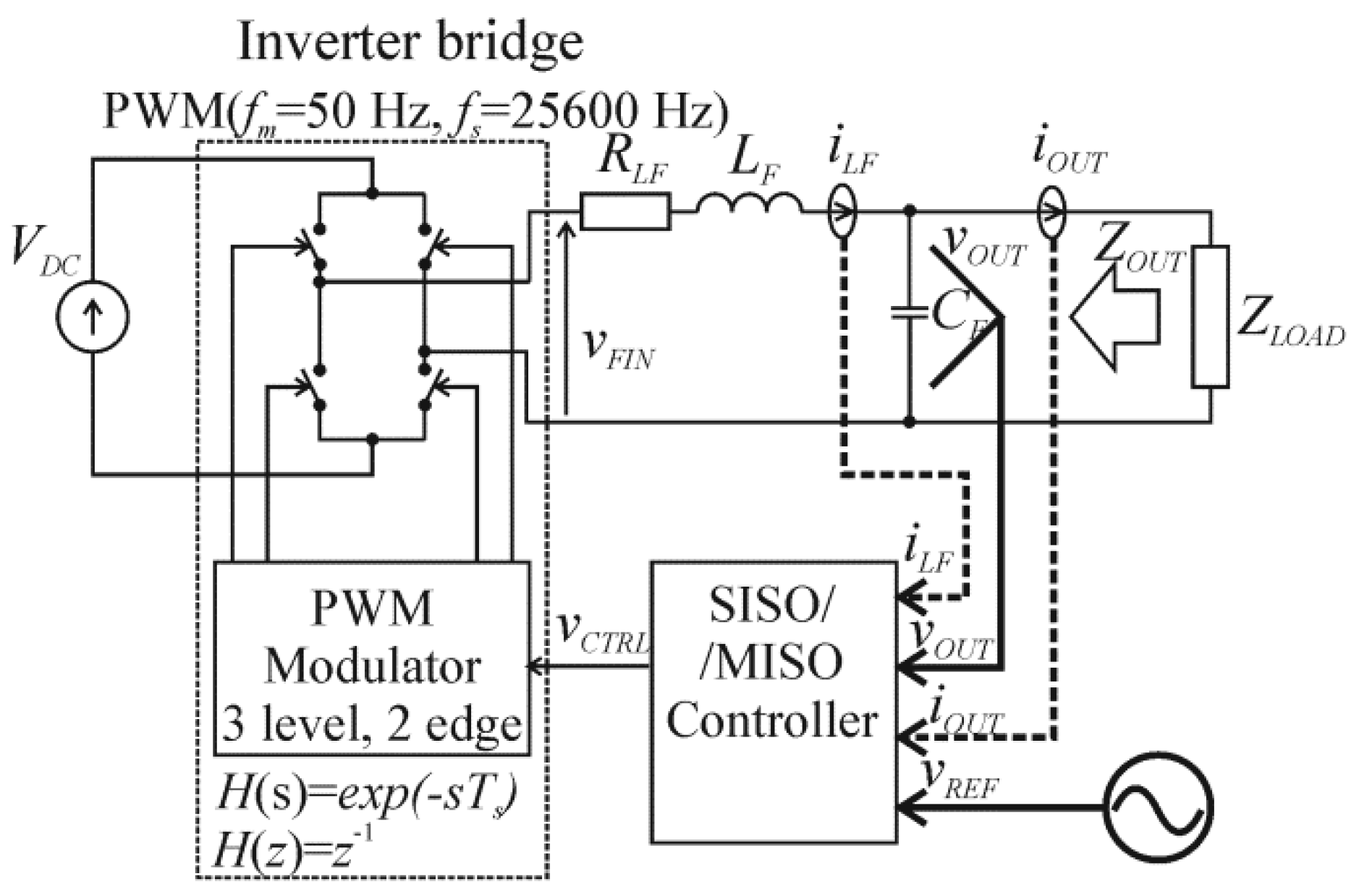
A much more sophisticated system is a multi-input single output (MISO) system (
Figure 1), in which the output current, the output filter inductor current, and the output voltage are measured and all of them are used as the input variables of the output voltage controller. In this case, the output current is also treated as a disturbance because the state-space matrix of the VSI does not depend on the particular load. However, in the case of MISO, we measure the output current (treated as a space variable or a measured disturbance [
20]), which renders the problem of the missed feedback loop (output voltage—output current) unimportant.
The assignment of a linear or nonlinear plant model is the basic problem in control loop design. The inverter plant has some nonlinearity. The dead time
Tdt of switching transistors in the H-bridge is one of the reasons for distortions of the output voltage [
4] (a little step decrease in output voltage occurs when the inductor current changes direction) and can be taken into account in the nonlinear model of the inverter [
21]. However, for the standard
Tdt ≤ 0.5 µs (for Metal-Oxide Semiconductor Field-Effect Transistors MOSFET, it can be tens of ns) and for the switching frequency
fs = 20 kHz (switching cycle
Ts = 50 µs), the decrease in the fundamental harmonic of the output voltage is approximately only
Tdt/
Ts ≤ 1%. The problem of the influence of the nonlinear characteristic of the inductor in the inverter output filter on the design of the adaptive control loop (with calculation of the nonlinear inductance characteristic) is presented in [
22]. However, the change in the coil’s inductance and its equivalent serial resistance as a function of the amplitude and the frequency of its magnetizing current depends on the core material. For contemporary alloy-powder materials (e.g., Sendust (MS)/Super-MSS™ [
23]), the exemplary change of inductance is about 5%, and the equivalent serial resistance is low in the operating point [
24]. Therefore, it has no serious impact on the VSI model. The solution of the state-space equations of the pulse width modulation (PWM)-controlled VSI results in the nonlinear (exponential) dependency of the state-space variables on the switching on (duty) time [
25]. In [
26], the nonlinear control function is approximated by the Fourier series. The nonlinear modeling of the inverter using Hammerstein’s approach (by means of the black-box identification method) is presented in [
27]. All the approaches that take into account the nonlinearity of the inverter slightly increase the accuracy of its modeling; however, it has been shown that a linear approximation of VSI results in quite a satisfactory compatibility of the linear theory and the experimental model measurements and enables the easily understandable design of the control loop. Modeling the inverter as linear was practiced for many years (e.g., [
1]) and resulted in the control design keeping low distortions of the output voltage for standard loads. We do not consider the thermal dependencies of the inductance, assuming that we work in standard ambient temperature conditions and that self-heating results in a stabilized temperature of the coil.
Estimating the quality of the VSI output voltage is also a challenge. The most common method for estimating static load distortions of the output voltage is to use the total harmonic distortion (THD) coefficient, which is simply the ratio of the root mean square (RMS) value of a set of the higher than the first harmonics of the output voltage to the RMS value of the fundamental harmonic. The problem is that this is an averaged value and the spectrum of harmonics cannot be discussed using it. The distortions of the VSI output voltage after dynamic load changes [
19] are defined by means of the over- or undershoots of the output voltage and the settling time. There are some approaches that use wavelet analysis to present more complex distortions of the output voltage [
28]. In systems with a discrete-time pulse width modulation (PWM) control, in which the delay of some (at least one) switching cycles is unavoidable, the output voltage over- or undershoots are mainly the result of an insufficient capacitance in the VSI output filter (the feedback loop is important but to a lesser degree) because the system works in at least one switching period after the step decrease/increase in the load without control. For a sufficiently high output filter capacitance value, all of the properly designed SISO and MISO controllers reduced the distortions of the output voltage for the dynamic load to a similar degree. However, the settling time was different. Therefore, it seems that the most significant comparison of controller features can be done using a nonlinear RC load. A comparison of the distorted input inverter DC voltage in the case of the cooperation of a VSI with an impedance network for the discontinuous current mode (DCM) of a network was previously presented in [
7]. Because the THD or the weighted THD (WTHD) [
29] coefficients only show the averaged values, we will now analyze the spectrum of the harmonics of a single-phase VSI with selected control systems and attempt to determine which spectrum is the most appropriate for controlling a VSI. The newly defined control quality factor (CQF) will be used in order to permit a clear estimation of the SISO and MISO controller properties (
Figure 1).
Section 2 presents an analysis of the frequency range, in which the features of the controllers will be compared when considering the magnitude of the VSI output filter.
Section 3 presents the approach to the discrete-time modeling of the VSI.
Section 4 presents the exemplary SISO controllers of the VSI, and the MISO passivity-based control (PBC) PBC-IPBC2 is described in
Section 5. Special attention was paid to selecting the PBC gains that were used in the simulations.
Section 6 is devoted to a comparison of the SISO and MISO controllers for standard loads using an experimental VSI model. The main aim of the paper is to determine which type of control loop is more suitable for each particular type of standard load (static, dynamic, nonlinear rectifier RC load).
2. Analysis of the Frequency Range of the Controller Features
The transfer function of a simple continuous SISO model (
Figure 1) of VSI (
Figure 2) is calculated in Equation (1). Let us assume that in the steady state
VOUT =
VREF and
kV = 1.
In the simplified continuous model (
Figure 2), for
Ts <<
Tm (switching period
Ts, fundamental period
Tm), we can omit the delay, exp(−
sTs), of the PWM modulator (
Figure 1). The transfer function of the changes
ΔVDC in the
VDC voltage supplying the VSI can decrease the result of the distortion of the DC voltage from the impedance network [
6,
7]. The output impedance of the VSI without a feedback loop
ZOUT is calculated in Equation (2), where
RLF is an equivalent serial parasitic resistance of the VSI bridge and the filter choke. In further calculations, we will assign
kV = 1.
We neglect the equivalent serial resistance (ESR)
RCF of the capacitor C
F. There is a problem with estimating the damping coefficient
ζF when a load current is modeled as an independent current source. Therefore, the damping coefficient
ζF will be calculated in Equation (3) for a case in which the nominal load resistance
RLOAD is present in the transfer function of the VSI. For
RLF <<
RLOAD, the output filter transfer function is calculated in Equation (3),
For the low-frequency range below
ωF0 (the resonant frequency of the output filter
LFCF), the output impedance of the VSIs without feedback loop
ZOUT, the transfer functions
FLC, and
Flf (
Figure 2) are calculated in Equation (4),
The transfer function of the output current, which is treated as an independent disturbance for the low-frequency range, lower than
ωF0 is calculated in Equation (5)
,The transfer function of DC voltage change
ΔVDC for the low-frequency range
ω <<
ωF0 and
kV = 1 is calculated in Equation (6),
The specific case shown in Equation (7) is for
ω = ωF0, and the values of
LF = 1 mH,
CF = 50 μF, and
RLF < 1 were used.
The transfer function of
ΔVDC for the low-frequency range
ω =
ωF0 and
kV = 1 is calculated in Equation (8),
For the high-frequency range over
ωF0, the output impedance
ZOUT of the VSI without the feedback loop and the transfer function of the output current (which is treated as an independent disturbance) for the high-frequency range over
ωF0 is calculated in Equation (9). We assume that filter
FLC(
jω) for ω >>
ωF0 damps the signals of whatever is the transfer function
Flf(
jω) (|
Flf(
jω)| ≤ 1).
The transfer function of
ΔVDC for the high-frequency range
ω >>
ωF0 and
kV = 1 is calculated in Equation (10),
Equations (9) and (10) mean that for ω >> ωF0, the output impedance of the VSI with the feedback loop and the transfer function of ΔVDC with the feedback loop are not dependent on it.
It can be seen from the presented Equations (1)–(10) that the gain of the controller is important in damping the disturbances for the resonant frequency
ωF0 and below this frequency of the output filter. For the higher frequencies, it is not important because of the high suppression of the output filter. This discussion, which is based on
Figure 2, led to the further investigation of controller properties being carried out in the 2
ωF0 frequency range.
3. Discrete-Time Modeling of the Voltage Source Inverter
Today, only the digital control of VSI is important. Every PWM discrete-time modulator implements one switching period delay
Ts (the data are written for the modulator in one switching cycle, and the pulse width is set in the next cycle). For VSIs that are used in UPS systems, the requirement of low output voltage harmonics has made the sinusoidal PWM the most popular. In the case of a single-phase VSI with a four-transistor, three-level H-bridge, a double-edge PWM is usually a sufficient solution. The design of the discrete-time controller requires that a discrete-time or continuous model of a VSI be used. The first approach is based on the continuous to discrete-time transformation (the discretized plant) using the zero order hold (ZOH) model or the Tustin model [
4,
30]. The second approach is based on solving the state-space equations (the discrete plant) and linearizing the control function [
1,
21,
30]. The third approach is based on the continuous model of a VSI, adjusting the quasi-continuous-time counterpart of the discrete-time controller, and finally, using a discrete-time controller (the discretized controller) [
8,
9]. The first and third solutions are based on the averaged models. The second solution considers the PWM features that distinguish the single and double-edge PWM. However, for a relatively high switching frequency, all of them gave similar results of control. The state variables
x = [
vOUT iLF iOUT]
T, the control (input) variable u =
vFIN, the output variable y =
vOUT (
Figure 1), and the state A and control B matrixes were calculated in Equation (11) when the ESR of the capacitor was neglected. The state-space equations
were solved for the time period of the switching on
TONk (
VFIN =
VDC) and switching off
TOFFk (
VFIN = 0). However, we obtained nonlinear equations for the control, so the discrete-time control matrix G
D was approximated exp(A
TONk/2) ≈ I + A
TONk/2 to linearize them [
1,
16,
25]. Finally, the discrete-time state-space equations were obtained, as shown in Equations (11)–(15) [
4,
21,
30].
The damping
ζF calculated from the space Equation (14) was not dependent on the load
ZLOAD (
Figure 1) because if
IOUT was treated as an independent current source (
Figure 2), the load was absent in the space equations. This is the difference in the Equations (16) and (3) describing
ζF value.
The output voltage discrete-time transfer function for the open loop is a control function of the duty cycle, which is controlled by
vCTRL and a function (−
ZOUT, where
ZOUT is an output impedance) of the output current Equation (17). The discrete-time control transfer function of a VSI Equation (24) considers an additional delay of one
Ts of the discrete-time modulator
H(
z).
For the open-loop system, Equations (18) and (19) are used:
Similar results of the discrete-time model for a VSI can be achieved using the c2d MATLAB function with the simplest ZOH discretization [
30] or the discretization in the analytic way [
8,
9].
4. SISO Control of a VSI
The first presented example of an SISO control is a modern discretized PID controller (presented in detail in [
8,
9]), which uses the simplest SISO model from
Figure 2 but includes an
RLOAD. The quasi-continuous transfer function [
8,
9] of the plant
Kp(
s) (including
RLOAD), considering a further ZOH discretization and one
Ts delay of the modulator, is shown in Equation (20),
The discrete-time PID controller is as in Equation (21),
The difference control law for
kV = 1 is as in Equation (22),
For the experimental model:
Ts = 1/
fs = 1/2,5600 s,
LF = 1 mH,
CF = 50 μF,
RLF = 1 Ω,
RLOAD = 50 Ω; the PID controller transfer function from [
8] will be
b0 = 18.014,
b1 = 33.495,
b2 = 16.094. These coefficients were analyzed based on the root locus [
8]. In Reference [
9], these coefficients were slightly adjusted:
b0 = 18.381,
b1 = 34.179,
b2 = 16.423.
The concept of a Manabe CDM [
10,
11,
12,
31] design of the controller (
T,
S,
R) is such that the coefficients of the closed-loop characteristic polynomial have assumed values, in the simplest case, of Standard Manabe Form. For
kv = 1 (
vREF is properly scaled), the output voltage of a closed-loop system is as in Equation (23),
The characteristic equation of a closed-loop system is as in Equation (24),
From Equation (18), Equation (25) can be derived:
For a system with a disturbance (in our case
IOUT), the degrees of R and S are equal to or higher than
n−1, where
n is the degree of
D. In our case, we will assume Equation (26):
The Diophantine Equation (27) should be solved for
r0 =
p0 = 1.
To solve Equation (27), Equation (28) should be solved to obtain the
ri and
si coefficients,
where Equation (29),
The coefficients
pi of Standard Manabe Form in a continuous system for the 5th degree of
P(
s) are the following:
where
τ is the time constant of a closed-loop system. Satisfactory results of the control of the experimental model were achieved for
τ = 4
Ts and for
τ = 5
Ts.
Let us define the following discrete-time transfer function using the
c2d function with the discretization cycle
Ts = 1/2.5600 s and the default ZOH method Equation (30) [
4]:
For τ = 4 Ts:
pz0(z0) = 1, pz1(z−1) = −1.327, pz2(z−2) = 0.6811, pz3(z−3) = −0.1826, pz4(z−4) = 0.0381, pz5(z-5) = −0.006738.
This last calculation enables
vOUT =
vREF to be kept in the steady state Equation (31).
For the experimental model, the solutions of Equations (28) and (31) were:
r0 = 1, r1 = 0.5898, r2 = 0.4218, s0 = 29.5050, s1 = −24.2037, s2 = −0.4607, t0/VDC = 0.1713.
However, in many cases
t0 is adjusted individually. The difference control law for
kv = 1 is as in Equation (32),
5. MISO Control of VSI
MISO controllers with multiple controller inputs, i.e., the output voltage, filter inductor current, and output current, and a single output, i.e., voltage (
Figure 1), effectively reduce the distortions of the output voltage for the different types of loads that are defined in [
19]. One of the MISO controls that is described often lately is the passivity-based control (PBC) presented by Ortega [
33] in 1989. PBC seems to be one of the best solutions for power conversion systems such as VSIs [
20,
34,
35,
36]. A VSI is presented as an energy transformation multiport device [
37]. If the stored energy is less than the supplied energy, the system is passive. The “injection” of the appropriate damping [
34] is basic for the control of the inductor and output currents; however, in the so-called improved PBC [
34], there is direct feedback from the output voltage. The state variables that define the energy of the VSI are defined as in Equations (33) and (34). The output current, which does not exist in the function of the system energy, is treated as an independent disturbance [
20].
The total energy that is stored in the system is described by the Hamiltonian function
H(
x) in Equations (35) and (36),
The error vector
e is defined as Equations (37)–(39),
vOUTref is the reference, sinusoidal output voltage waveform;
iLFref is the calculated reference current of the inductor.
The equilibrium of a closed-loop system is asymptotically stable [
38] and is achieved if
H(
e) has a minimum in
x = x
ref in Equation (40),
The system is passive if the time derivative
H(e) is negative in Equation (41),
Two equations are used—the first for a closed-loop system Equation (42) [
20] and the second for an open-loop system, as in Equation (43),
where the interconnection matrix,
J, and the damping matrix,
R, can be defined as in Equation (44),
Ra (the PBC controller) is the matrix Equation (45) of the injected damping,
Ri is the gain of the current error, and
Kv is the conductive gain of the voltage error.
Subtracting Equation (42) from Equation (43) results in the control law Equation (46),
For
vCTRL =
mVDC, the difference control law of a single-phase VSI with a PBC is shown in Equations (47) and (48),
The inductor current is an integral of a function of the output voltage, which is important for the steady-state error in the control law. The adjustment of the PBC gains,
Ri and
Kv, is a problem. The matrix
R +
Ra should be positively defined to fill this requirement Equation (41) [
20]. In practice, this means that
Ri +
RLF and
Kv should be positive. Calculating the upper restrictions of their values can be difficult [
34]. The higher their values are, the higher the convergence of the error tracking is. The characteristic polynomial of a closed-loop system with a PBC is shown in Equation (49),
The roots
λ1,2 Equation (50) of the characteristic polynomial Equation (49) of a closed-loop system Equation (42) will always have the real part negative (
Figure 4a,b) for the positively defined
R +
Ra matrix.
However, in the simulations and in the experimental model, overly high values of
Ri and
Kv led to oscillations in the control voltage and output voltage (
Figure 5). An overly high value of modulation index
M [
39,
40] for the nonlinear rectifier RC load led to the saturation of the PWM modulator (
Figure 6). Both of these cases produced the same result. The reason can be the disability of fast current changing in the filter inductor [
40]. Therefore, the best adjustment of the PBC controller gains
Ri and
Kv is to determine the lowest THD (for the nonlinear rectifier RC load).
Figure 6 presents two problems. The first is saturation in the PWM modulator due to overly high values of the PBC gains (
Ri and
KV). The second case can be presented comparing the root loci from
Figure 4a,b and
Figure 6. For
Ri = 10, oscillations can occur for
KV = 0–1, for
Ri = 20, and for
KV = 0.5–1.5. The second problem was not so important. The value of
M = 0.3 was too low in practice. It was experimentally checked in the VSI model and finally set at
M = 0.8,
Ri = 5, and
KV = 0.5. The equations from the literature did not solve the problem of restricting the upper
Ri and
KV values. From
Figure 5, it is obvious that an MISO control with a low
M value is able to efficiently control the output current. The presented PBC control was further named IPBC2 because compared to the basic PBC theory [
34], it used the output voltage as in [
34] and its derivative in the final control law. This derivative was absent in the improved PBC (IPBC) that was presented in [
34].
The idea of the calculation of the upper limit of
Ri gain was presented in [
34]. The derivative of the control voltage
vCTRL in one switching cycle should be lower than the maximum carrier slope in the PWM modulator. For the double-edge modulation and recalculating it to the DC voltage level, it is equal to
VDC/(
Ts/2) [
34]. However, it is shown in
Figure 5 and
Figure 6 that the mutual dependency of the two PBC controller gains is very important. In one sampling period, we can assume d(
vOUTref)/d
t ≈ 0. Therefore, from Equation (48) we can calculate:
From Equations (47), (51) and (52), we can calculate Equation (53):
In one switching cycle, for
RLOAD = ∞, we can assume Equation (54):
The final restriction of PBC gains,
Ri and
Kv, from Equation (55) is Equation (56),
The restrictions of the operating area, shown in
Figure 7, can be one of the reasons for the THD increase in the higher values of PBC gains presented in
Figure 5 and
Figure 6. However, Equation (56) does not consider the modulation index
M value because the maximum carrier slope does not depend on
M (the reference voltage depends on
M). Equation (56) is calculated for
RLOAD = ∞, while the restrictions of the
Kv value for the existing load resistance will be slightly lower.
6. Comparison of Experimental Voltage Source Inverters with PID, CDM, and PBC Control Systems
The comparison of the SISO-PID (the version from [
8,
9]), SISO-CDM, and MISO-PBC-IPBC2 systems was based on measurements of the VSI output voltage for standard loads.
Figure 8a–d presents the output voltage for the standard [
19] nonlinear rectifier RC load for
R = 100 Ω and
C = 430 μF. The vertical axis of
Figure 8a–d is scaled in units of the 13th bit bipolar Analog To Digital Converter ADC. The actual voltage amplitude was about 60 V. The output filter (
LF = 1 mH,
CF = 50 μF) resonant frequency was about 712 Hz. The initial analysis (
Section 2) showed that the feedback loop is only important for the neighborhood of this frequency (about 14th harmonic) and below. Therefore, a sufficient frequency range for comparing the controllers was from the 2nd up to the 30th harmonic.
Figure 8a–d presents the output voltage waveforms without feedback and with the PID, CDM, and PBC-IPBC2 controllers. The THD coefficient was calculated for each case. The PID and CDM controllers had similar THD, while for the PBC, it was a bit lower. However, the output voltage waveforms were different. The harmonics spectra are presented in
Figure 9a–d. It can be noticed that the harmonics spectrum is different for the different controllers. Some of the harmonics are increased (e.g., the 2nd harmonic for the CDM controller increased because the voltage waveform was not ideally symmetrical). The importance of a decrease or increase in a specific harmonic was dependent on its relative amplitude. Therefore, the influence of the feedback loop on the particular harmonic can be defined as in Equation (57),
where
hNFBn is the n-th relative harmonic amplitude of the output voltage without feedback and
hCTRLn is the n-th relative harmonic using the selected controller. The sum of the
xn values is a measure of the feedback quality. The better the quality, the higher the value of the coefficient. Therefore, the final definition of the control quality factor (
CQF) is as in Equation (58),
where
m is the harmonic order above the filter resonant frequency, in our case
m = 30.
The higher the
CQF, the better the control. It can be seen from
Figure 8a–d that for the nonlinear rectifier RC load, the best controller was the PBC (
CQF = 1.51), the second best was the CDM (
CQF = 1.41), and the third best was the PID (
CQF = 1.2). The
CQF measure enabled us to distinguish the quality of PID and CDM controls that had almost the same THD. The nonlinear load caused harmonic disturbances, and the
CQF was the proper measure of their damping.
The quality of the control should also be determined for a dynamic load change.
Figure 10a–d shows the over-and undershoots after a dynamic load decrease and increase (45 Ω to 500 Ω and 500 Ω to 45 Ω) and the settling time. The lowest over- and undershoots (about 3% and −2%) were for the CDM control, the shortest settling time (about 1 ms in both cases) was for the PID control, and the worst parameters were for the PBC-IPBC2 (about 6% and −5.1%, 3.5 and 2 ms). It would be difficult to improve the dynamic properties of the PBC because increasing the gains
Ri and
KV would lead to higher oscillations and a longer settling time, while decreasing them would lead to higher over- and undershoots. In the PBC, we directly control the filter inductor current as in Equations (47) and (48) but the inductance disables fast current changes, which can lead to the saturation of the modulator. The capacitance in the output filter has a significant influence on the over- and undershoots.
9. Conclusions
A comparison of SISO-PID, SISO-CDM, and MISO-PBC-IPBC2 systems showed that for the nonlinear rectifier RC load defined in the IEC 62040-3 standard [
19], the best results (the lowest distortions of the output voltage) were for the PBC-IPBC2 controller that had the gains adjusted after the initial simulations (
Figure 5,
Figure 6 and
Figure 7). The measurement of the currents enabled them to be better shaped (
Figure 5). A new control quality factor was defined and enabled a better resolution in the description of the control results. An analysis of the root locus (
Figure 4a,b) showed that the voltage source inverter with the PBC-IPBC2 control should always be stable for any positive gains
Ri and
KV; however, the simulations (
Figure 5,
Figure 6 and
Figure 7) and measurements of the experimental model showed that oscillations in the output voltage existed for the higher values of gains. It is obvious that the MISO-PBC-IPBC2 system with the output current and filter inductor current measurements better damped the important harmonics (
Figure 9a–d). The output voltage parameters (the over- and undershoots, the settling time) for the linear dynamic load were worse for the PBC-IPBC2, and we were not able to improve them by changing the values of the controller gains. An increase in the gains decreased the over- and undershoots but increased the settling time because of oscillations. The reason for the worse dynamic response of the PBC could be the direct control the filter inductor current, during which the inductance disables fast current changes, which can lead to the saturation of the modulator [
40]. The static error, which was calculated as the decrease in output voltage amplitude after an increase in the load (500 to 45 Ω), was low and was similar for all of the controllers (about 2% vs. 4% without feedback), which is understandable because the static error was mainly reduced by the integration action of the output voltage. All of the controllers had such an action (the PBC-IPBC2 controller due to the control of the inductor current, which was dependent on the integration of the function of the VSI output voltage). All of the controllers cause small oscillations (
Figure 10a–d) in the VSI output voltage (in the experimental model) close to the zero crossing, which could have been the result of the wind up effect of the controller (the voltage error was integrated, and the three-level PWM for the voltage crossing zero was not able to control the output voltage efficiently with very short pulses). To summarize, in the case of a nonlinear load, the more expensive MISO-PBC-IPBC2 controller had much lower distortions of the VSI output voltage, while in the case of dynamic loads, the less expensive SISO-PID and SISO-CDM controllers were sufficient and the static error was the same for all the controllers. Therefore, the final selection of either a simple and inexpensive SISO with one measurement trace or an expensive MISO with three measurement traces depends on the proposed function of the VSI.


