Article

An Analog Magnetic Isolator for Space Power Applications

Power Supply Systems Group, University of Oviedo, 33204 Gijon, Spain
*
Author to whom correspondence should be addressed.
These authors contributed equally to this work.
Energies 2020, 13(17), 4504; https://doi.org/10.3390/en13174504
Submission received: 28 July 2020 / Revised: 19 August 2020 / Accepted: 21 August 2020 / Published: 1 September 2020
(This article belongs to the Special Issue Advanced Space Power Systems)

Abstract

:
In power electronic applications, often a galvanic isolation barrier has to be passed. An example of this is the feedback control of isolated DC/DC converters where the secondary voltage has to be passed to the primary side where the control circuitry lies. For these applications, the use of optocouplers is well known in terrestrial applications. However, optocouplers tend to suffer degradation from the radiation damage induced by the space environment. For this reason, some space grade DC/DC converters use some form of magnetic feedback. In this paper, a magnetic analog isolator is presented. It will allow for passing an analog voltage through an isolation barrier by means of a magnetic transformer based circuit. It will be based on an LLC DC/DC converter so the gain between both sides of the isolator can be tuned. Design methodology will be presented so the circuit can be tailored for any foreseen application. In this paper, a simulation of its application in a Latching Current Limiter is presented. All the components will be discrete components which have a rad-hard version. A design example having a bandwidth around 20 kHz and a gain of 4.6 dB is shown in the Experimental Results sections to support the analysis.

1. Introduction

Space electronics have to work in a very harsh environment facing extreme temperatures and high radiation doses. Furthermore, space equipment must work for many years in such a extreme environment without maintenance. For this reason, the design has to be very hardened and sometimes deviates from common designs in small details. One of such details is how to pass a galvanic isolation barrier. For example, to pass to the PWM modulator, controlling the switches of an isolated converter, the duty cycle information if the controller lies in the secondary part of the transformer. In terrestrial applications, optocouplers are usually the first choice. However, optocouplers have many limitations. Some are well known in terrestrial applications such as Current Transfer Ratio (CTR) variation, noise, and low bandwidth. However, others are more specific to space and radiation applications. With the radiation induced degradation, the CTR diminishes a lot [1,2], so the converter control loop has to compensate for that. In order to compensate for these effects, transformer-based magnetic feedback have been proposed and implemented. For example, Rad-Hard DC/DC converters from Microsemi [3] have this feature. Magnetic feedback has also been used in terrestrial DC/DC converter applications and there are integrated circuits that are used for this purpose [4]. However, to the best knowledge of the authors, besides [5,6], no specific designs have been proposed. In this paper, an analog isolator design based on a resonant DC/DC converters is proposed. The bandwidth achieved is in the range of the tens of kHz and they can offer a voltage gain wide enough to be adapted to many requirements. Furthermore, design guides to achieve a flexible design will be provided. This isolator will be capable of driving the gate of a power MOSFET operating as a current source. All the components are discrete ones and almost all of them belong to the European preferred parts list [7].
The paper is organized as follows: Section 2 shows the background and design of the analog isolator, Section 2.3 shows one application driving the requirements or the design. The design of the circuitry is described in Section 3, and special care has been taken for the analysis of the resonant network in Section 3.1.2. A design procedure, verified by simulation, is shown in Section 4.1, and the results can be found in Section 4.2. Finally, conclusions are addressed in Section 5.

2. Design of the Analog Isolator

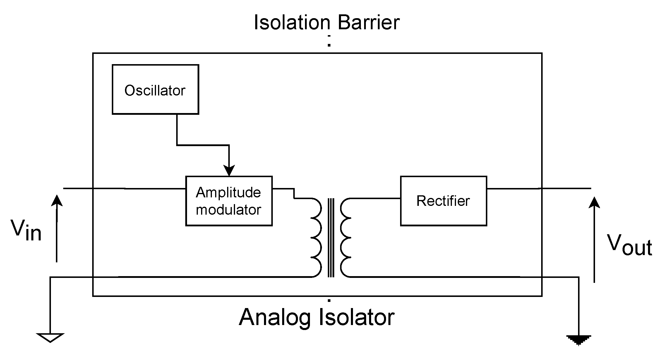
2.1. Concept and Reference Designs

The overall design of the analog isolator is depicted in Figure 1. The signal to be transferred is called V i n . Let us call the primary side of the analog isolator where V i n drives an amplitude modulator generating an AM modulated carrier. This AM modulated carrier is transferred through a magnetic transformer, being the primary of the magnetic transformer connected to the primary side of the isolator and the secondary of the transformer to the secondary side of the isolator. The AM modulated carrier will be demodulated with a rectifier, obtaining V o u t which would be a scaled version of V i n , thus the information contained in V i n (e.g., the output voltage of an isolated converter to be controlled, the control action to be performed, a measurement, …) is recovered at the secondary side of the isolator.
The same concept is implemented in [5,6]. In both cases, the modulation stage derives from a DC/DC converter. In [6], the isolator is based on a forward converter operating at fixed frequency and duty ratio. The input voltage of this Forward converter is the signal to be transferred V i n , therefore the audio-susceptibility of the Forward converter is used to transfer V i n .
In [5], the AM modulator concept is also used, but it is performed in a different way. The isolation is performed by a Flyback transformer driven by a pulsed current source. To be consistent with the primary and secondary terminology, let us call the side of the transformer driven by the current source the secondary, but in a typical Flyback converter it would be the primary. This current source operates with a fixed frequency and duty ratio, and it is constant in amplitude. The voltage modulation is performed by fixing with V i n the Flyback rectifier output, which in this case should be called the primary. Thus, when the transformer has to be demagnetized, it will do so with voltage V i n which appears at the other side where it is sampled obtaining V o u t .
It is important to note that the magnetic isolation concept have been incorporated to integrated circuits such as the UC1901 [8], in which the transformer is external. Another example with an internal transformer is Analog Devices ADUM3190S [9]. Both devices are available as space grade options. However, for certain applications, they might be a little limited. For example, ADUM3190S requires an isolated power supply for the secondary side and the output voltage range of UC1901 can be very small for certain applications. For these reasons, a fully discrete and custom circuit that can be adapted to many input–output voltage ranges is presented here. However, for the target applications of the aforementioned ICs, they excel and surpass the capabilities of the approach presented in this paper.
This paper uses a similar approach as [6], thus no power supply is needed for the secondary of the isolator. A DC/DC converter will be used with a fixed switching frequency and duty ratio. The input voltage will be V i n . However, in this case, it will be based on a resonant DC/DC converter very similar to the well-known LLC converter. This topology will be described in Section 3. It uses a half-bridge for driving a resonant circuit which includes a magnetic transformer that provides the isolation. The advantages of using a resonant converter are various. First, the transformer is AC driven since C t a n k blocks any DC voltage applied, so its magnetic material cannot saturate avoiding all the process described in [5] to avoid transformer saturation. Second, Zero Voltage and Zero Current switching can be achieved, thus a high frequency switching can be used maximizing the small-signal bandwidth of the V i n to V o u t transfer functions. For the proposed design, switching frequencies in the MHz range will be preferred. Third, as the currents through most of the devices are sinusoidal, the EMI problems should be small so the spectral content will be minimized. However, the use of a resonant DC/DC converter topology is not without problems. All the elements of the resonant network and the transformer have to be carefully selected and designed. The inductor and capacitor values forming the resonant network have an impact in the V o u t / V i n ratio so it can be adjusted at the designer’s will. These issues will be addressed in Section 3.1.2.

2.2. Space Qualified Components’ Restrictions

The use of discrete components from the European Preferred Parts List [7] imposes several challenges. Primarily, the MOSFETs that appear are high power devices not suitable for high frequency switching. Thus, all the transistors used will be bipolar junction transistors. Therefore, bipolar anti-saturation techniques will have to be implemented to enable switching at the MHz range. These techniques are described in Section 3.1.1.

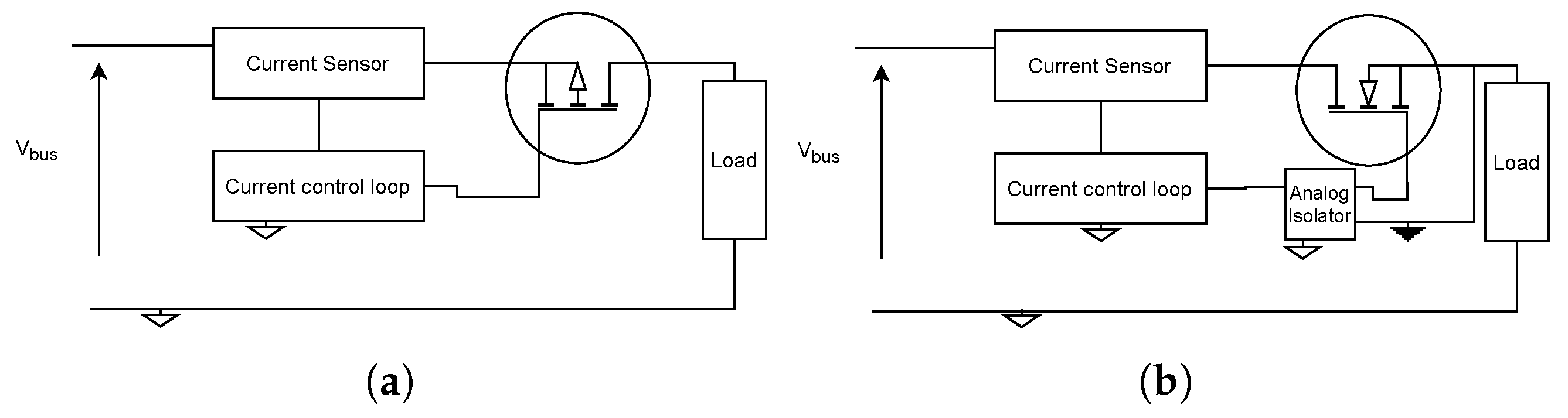
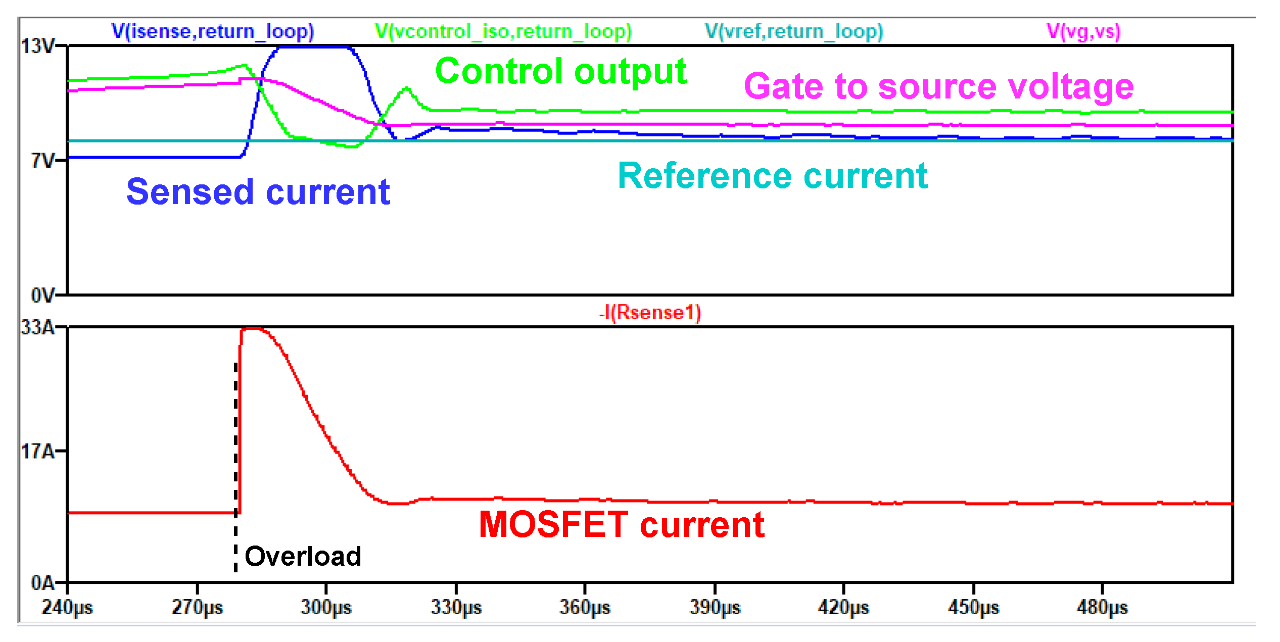
2.3. Application: Latching Current Limiters

One of the design drivers of these analog isolator is its integration in a Latching Current Limiter (LCL). LCLs are a protection device used by the European Space Agency (ESA) spacecrafts. They are designed to limit the current demanded by a load to a fixed value for a certain time, thus protecting the bus from an overload. If the time is elapsed the LCL deems that there was a failure and disconnects the load. They are also used as switches. Normally, the device that limits the current is a P channel MOSFET because the source will be connected to the bus side, and it is easily driven by the current control loop, which is referred to the ground of the spacecraft. Figure 2a shows a conceptual schematic of such device. A full description of LCLs requirements are recorded in [10] and a complete set of explanations can be found in [11].
However, N channel MOSFETs usually exhibit a lower on-state resistance so the ohmic losses in the device when it is not limiting the current would be lower than in a P channel device. However, the source of the N Channel device shall be connected to the load side and thus the control loop information has to be referred to the source of the MOSFET. Here is where the analog isolator comes into play, translating the control loop voltage, referenced to the ground of the spacecraft to the gate to source voltage of the MOSFET referenced to the source. Figure 2b shows a conceptual driving of an N channel MOSFET LCL with an analog isolator. For this application, ideally the secondary side of the analog isolator (see Figure 1) does not need a power supply. This rules out the use of the Analog Devices ADUM31190S. In order to minimize the on-state resistance of the MOSFET, the maximum output voltage provided shall be close to the maximum required gate-source voltage of a MOSFET with the derating provisions [12]. This means a gate-source voltage around 15 V . This is way above the capabilities of UC1901.
As the dynamic requirements of the LCLs are very stringent regarding speed response and loop stability, the frequency response of the analog isolator shall be carefully verified. However, the design of the analog isolator shall be flexible enough to be used in other applications such as the feedback loop of an isolated DC/DC converter or in a isolated sensor.

3. Proposed Design

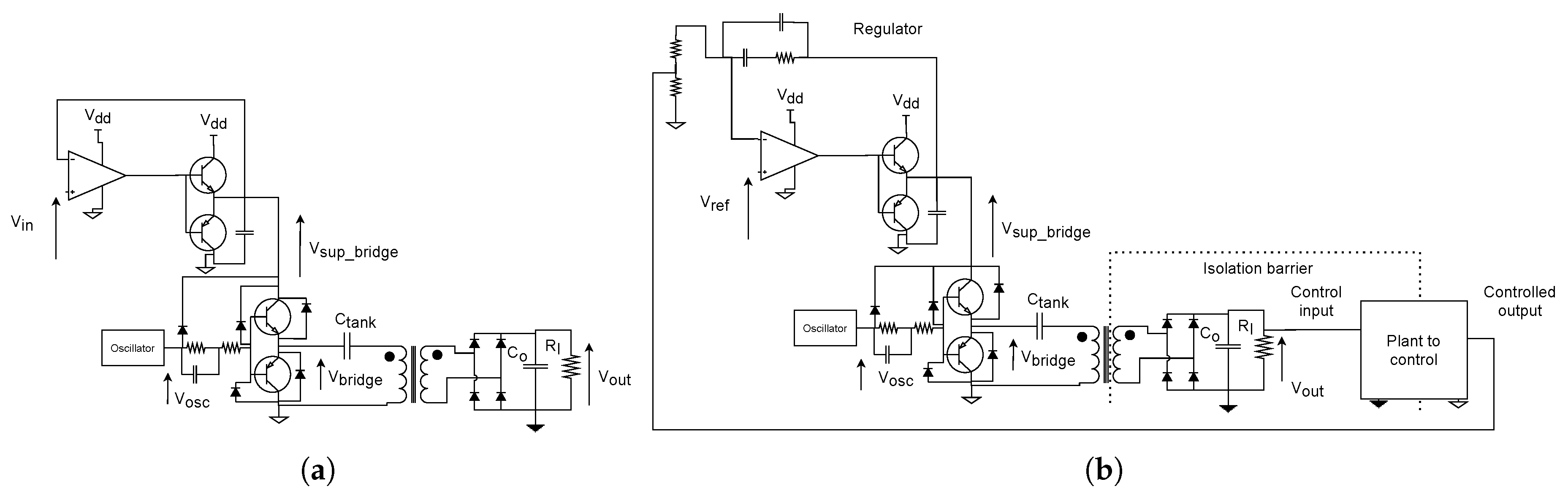
3.1. Isolator Design Description

The design of the analog isolator is depicted in Figure 3. A square wave oscillator, described in Section 3.1.1, drives a half bridge. This generates a square voltage waveform, V b r i d g e , at the input of a L C resonant circuit formed by C t a n k and the leakage inductance of the transformer. The current at the switching frequency is coupled to the secondary by means of the transformer, where it is rectified and low pass filtered. The whole design of the resonant network is explained in Section 3.1.2. The amplitude of V b r i d g e is controlled by means of its supply voltage V s u p _ b r i d g e , which is provided by the complementary linear stage; this is the amplitude modulator. Therefore, the information contained in V i n modulates the amplitude of V b r i d g e and after the rectification and the filtering in the secondary is recovered as V o u t . Therefore, V o u t is a scaled version of V i n . As described in Section 3.1.2, the scaling is achieved by the design of the resonant network. Figure 4 shows different configurations for the same principle. By placing an additional op-amp with the feedback for the amplifier at the V s u p _ b r i d g e the base-emitter junction voltage drop is compensated. Thus, V s u p _ b r i d g e follows V i n . If the analog isolator was going to be integrated in a control loop, the operational amplifier could be used for implementing the regulator transfer function. This is represented in Figure 4b. The output of the analog isolator is the control input to the plant (e.g., in an isolated DC/DC converter, it could be the duty cycle command). The control action will be implemented by the op-amp that sets V i n . It will sense the output of the plant, compare it against the reference V r e f , and decide which control action is needed to have the output of the plant following V r e f (e.g., in a isolated DC/DC converter, the controlled variable is often the output voltage.) Please note how the input and output of the analog isolator are referenced with respect to the plant to be controlled. If the plant was an isolated DC/DC converter, the control and the analog isolator input would be placed at the DC/DC converter secondary and the output of the analog isolator will be referenced to the DC/DC converter primary.

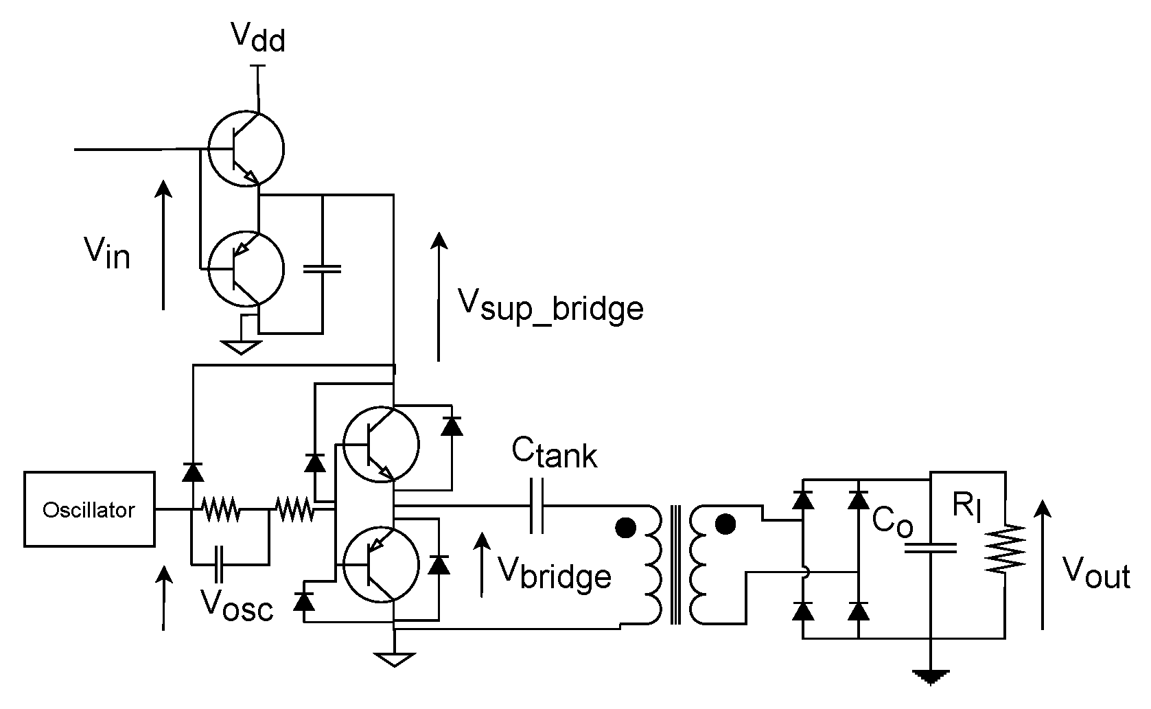
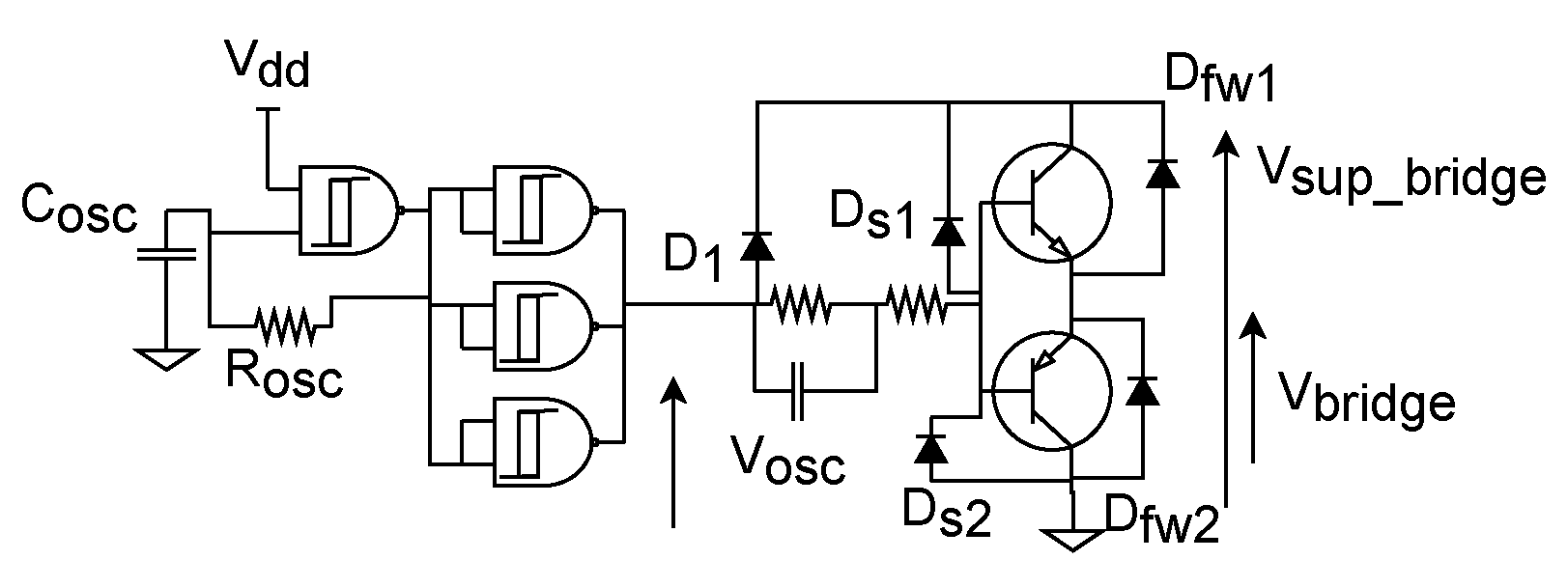
3.1.1. Oscillator and Transformer Driver

The design of the oscillator is depicted in Figure 5. A square waveform is generated by a NAND gate with Schimidt–Trigger input and a feedback network formed by R o s c and C o s c . The remaining input can be tied to positive as in the figure or to a control signal to turn on and off the oscillator. When this input is high, the NAND gate behaves as an inverter so when the voltage at C o s c is high, its output becomes low discharging C o s c , and, when it is low, the output becomes high charging C o s c . Therefore, R o s c and C o s c control the frequency of the oscillator. Additional gates configured as inverters provide more current to drive the half-bridge. They are implemented as NAND gates so a single chip with several gates could be used, in order to achieve a frequency in the MHz range provisions to avoid the deep saturation of the BJTs and to enhance the minority carrier extraction from the base. The latter is achieved by the presence of the capacitor connected in parallel to one of the base resistors that are needed. When V o s c is high, this capacitor gets charged. When V o s c is low, this capacitor imposes a small negative voltage in the base of the transistors.
Ideally, V o s c will have a maximum value of V d d . If by means of tracking V i n , V s u p _ b r i g e falls below V d d , the BJT collector–emitter voltage will be forward biased with a relatively high voltage, in order to prevent diode D 1 from clamping V o s c to V s u p _ b r i d g e . Diodes D S 1 and D S 2 further avoid the deep saturation of the BJTs. Finally, diodes D f w 1 and D f w 2 allow the reverse flow of the current through the bridge.

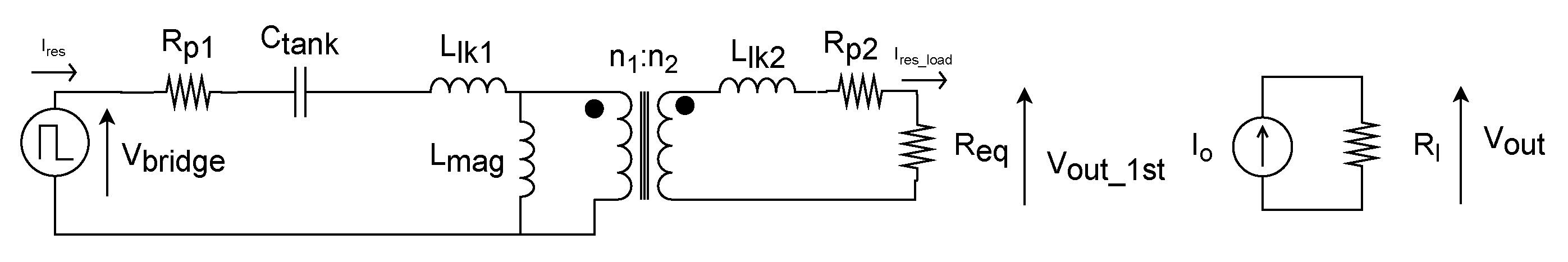
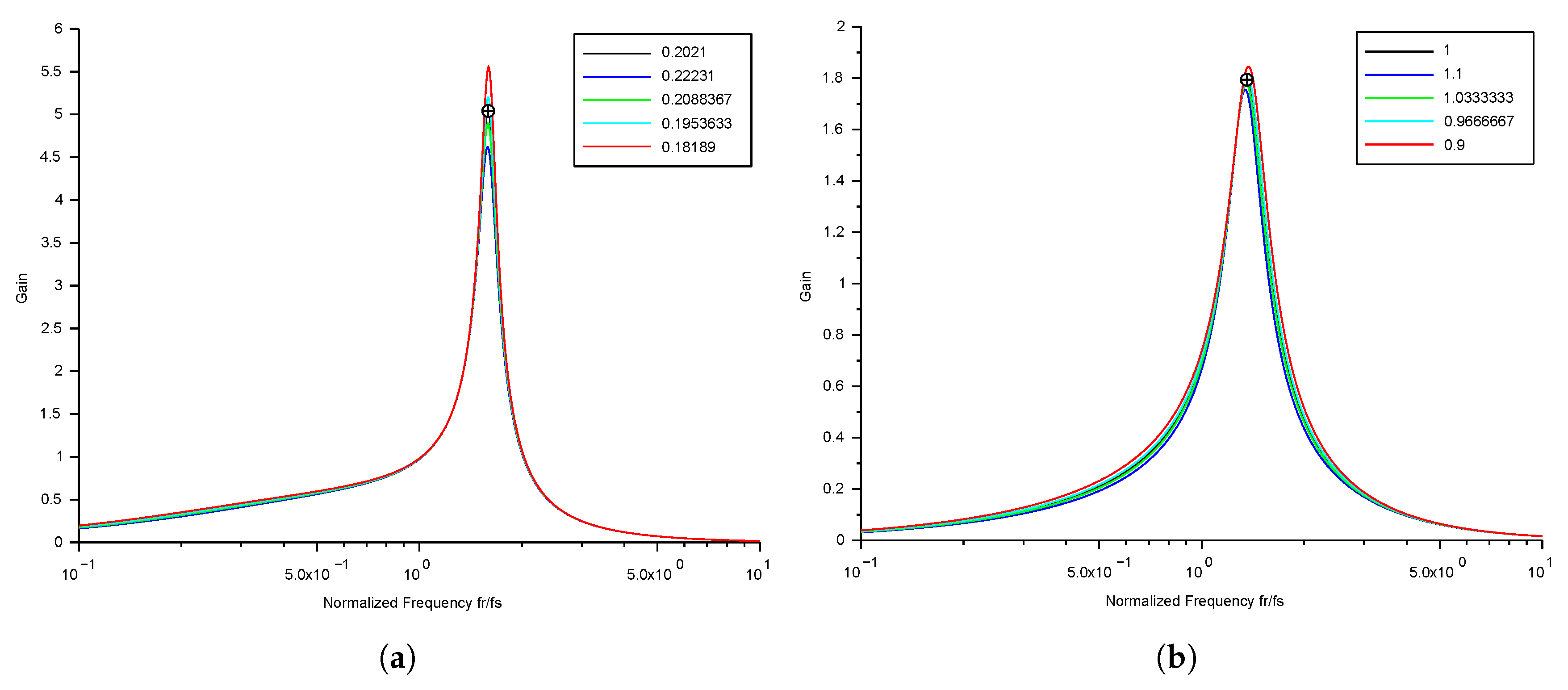
3.1.2. Resonant Network Design

The resonant network design plays a fundamental role in the static gain between V o u t and V i n . The procedure used to analyze and design is based on the First Harmonic Analysis (FHA), which is well referenced. The design of the LLC converter using FHA can be found in [13] or in the form of design guides in [14,15]. Basically, it will assume that, thanks to the resonant circuit formed by C t a n k and the primary leakage inductance L l k 1 , the only current that will circulate through the resonant tank, i r e s , will be due to the first harmonic, at the switching frequency f s , of the square voltage applied. The higher harmonics will generate no power at the output. In order to obtain this current, only the impedance of the reactive elements at f s has to be taken into account. However, most of the literature neglects the effect of the secondary leakage inductance, since in most transformers this value is very low in comparison to the magnetizing inductance L m . One of the exceptions is [16] in which it is taken into account since it is operating at very high frequency. In this paper, the analysis will include it, since the transformer is designed to have a big leakage inductance to use it in resonance with C t a n k . In addition, the parasitic resistances will be taken into account. Figure 6 shows the equivalent circuit for the FHA analysis. It can be seen how the bridge has been replaced by a square waveform voltage source that acts over a resonant network. The output voltage will be considered to be DC with negligible ripple thanks to capacitor C o . Then, the full wave rectifier makes the output capacitor and load behave as a resistor of value R e q with value [17]
R e q = 8 π 2 R l
The fraction of the resonant current i r e s that circulates through this equivalent resistor R e q will be called i r e s _ l o a d . It generates a sinusoidal voltage of amplitude V o u t _ 1 s t . This current will dissipate the same power at R e q as the DC current source of value I o over R l . Thus, by calculating i r e s _ l o a d , the DC output voltage V o u t can be inferred:
I o = 2 π · i r e s _ l o a d
V o u t = 2 π · i r e s _ l o a d · R l
The circuit in Figure 6 can be further simplified referring all the elements to the primary of the transformer, which can be done scaling it with the turns ratio n = n 1 / n 2 , with n 1 being the number of turns in the primary and n 2 the number of turns in the secondary. The result of the transformation can be seen in Figure 7.
In our design, n = 1 has been chosen to simplify the transformer design. The half bridge will generate a square voltage V b r i d g e between V s u p _ b r i d g e an 0 V. In order to calculate i r e s _ l o a d , the different reactive elements can be grouped. In Figure 7, they are grouped in three different impedances Z t a n k , Z e q , and Z s e c . Thus, in the frequency domain,
Z s e c = R e q + R p 2 + j · ω s · L l k 2
where ω s is the pulsation at the switching frequency f s . Z e q is then
Z e q = Z s e c · j · ω s · L m j · ω s · L m + Z s e c
and Z t a n k will be
Z t a n k = j w s · L l k 1 + 1 C t a n k · ω s
Z t a n k will be 0 at the resonant frequency f r
f r = 1 2 π 1 L l k 1 · C t a n k
In order to adjust the gain between V o u t and V i n , G i s o = V o u t / V i n , Z t a n k has to be properly chosen. This is accomplished by choosing the ratio between the resonant frequency of Z t a n k , f r , and the switching frequency f s , f r / f s ; thus, Z t a n k could be rewritten as
Z t a n k = j · ω s · L l k _ 1 1 f r f s 2
The other parameter affecting G i s o will be the quality factor, Q t a n k of the resonant network
Q t a n k = f r f s · ω s · L l k _ 1 R e q + R p 1 + R p 2
Solving the impedance divider, it is possible to obtain the ratio between the first harmonic of V b r i d g e , V b r i d g e _ 1 s t , and the amplitude of V o u t _ 1 s t , in absolute value is
G t a n k = Z e q Z e q + Z t a n k + R p 1 · R e q Z s e c = V o u t _ 1 s t V b r i d g e _ 1 s t
As can be inferred, G t a n k depends on the values of the primary and secondary leakage inductance of the transformer, L l k 1 , L l k 2 and the magnetizing one L m . The evaluation of G t a n k according to Equation (10) for the inductor values described in Section 4 can be found in Figure 8 for different f r / f s ratios and Q t a n k values. In Figure 8a, Q t a n k is varied around 0.2 whilst f r / f s varies from 1 / 10 to 10. In this gain, the maximum gain is close to 6. For the same f r / f s variation, Figure 8b shows the gain achieved with Q t a n k varying around 1. In this case, the peak gain is around 2. It can be seen how different gain values higher than 1 can be achieved by the right combination of f r / f s and Q t a n k . Having f r / f s bigger than 1 implies that the load seen by the half bridge is inductive. This will help discharge the parasitic output capacitance of the half bridge and have Zero Voltage Switching (ZVS) in the transistors [15].
The amplitude of the first harmonic of V b r i d g e can be calculated by decomposing a square waveform at frequency f s between V i n and 0 with duty cycle D into its Fourier series components
V b r i d g e ( t ) = V i n · D + k = 1 2 k · π sin ( k · π · D ) · cos ( 2 π · k · π · D · f s · t )
Therefore, with D = 0.5 , the amplitude of the first harmonic V b r i d g e _ 1 s t = V i n · 2 π . Then,
V o u t _ 1 s t = G t a n k · 2 π · V i n
and
i r e s _ l o a d = V o u t _ 1 s t R e q = G t a n k · 2 π · 1 R e q · V i n
Then, applying (1) and (3) V o u t is
V o u t = 2 π · i r e s _ l o a d · R l = 4 π 2 · R l R e q · G t a n k · V i n
and then G i s o = V o u t / V i n
G i s o = 1 2 · G t a n k
and for a square waveform with duty cycle D
G i s o = 1 2 · G t a n k · sin ( k · π · D )

4. Experimental Results

4.1. Design Procedure

The design of the analog isolator would be oriented to achieve a certain gain G i s o fixed at design stage so it could be integrated in the application. This gain would be achieved through the process described in Section 3.1.2. However, there are many degrees of freedom so the same goal could be achieved by several means. The process used for this paper is described below.
  • Choose a the switching frequency at least 10 times higher than the desired bandwidth. In this case, it was set to 4 MHz.
  • Design a transformer. The turns ratio will be 1. This will fix the values of L l k 1 , L l k 2 and L m which can be obtained by measurement or by simulation through a finite element analysis software.
  • Choose the desired G i s o and therefore G t a n k . Plot Equation (10) with different ranges of Q t a n k and f r / f s . The values of the resistances r p 1 and r p 2 can be approximated by the parasitic resistance of the windings plus the ESR of the resonant capacitor.
  • With G t a n k selected to achieve G i s o fix Q t a n k and f r / f s . The latter with the selected f s determines f r .
  • With f r and L l k 1 , select C t a n k using Equation (7).
  • With L l k 1 and f r , select R e q that guarantees the desired Q t a n k using Equation (9).
  • Transform R e q to R l using Equation (1) to finish the design.
In order to verify the resonant network design, a PSIM simulation was carried out. The design of the resonant circuit is based on having a Q t a n k = 0.2 . The switching frequency was fixed at 4.08 MHz with a duty cycle D = 0.5 and the objective is to achieve the maximum gain. Thus, f r / f s = 1.59 and then f r = 6.5 MHz. The transformer is characterized by L l k 1 = L l k 2 = 8.8 μ H and L m = 14.3 μ H with Parasitic resistances r p 1 = r p 2 = 1.12 Ω . In order to achieve the desired f r , then C t a n k = 68 pF and Q t a n k are guaranteed with a R l = 2.2 k Ω . Following Equation (10) and Figure 8a, it is possible to derive a value of G t a n k = 5.04 , thus achieving G i s o = 2.52 . Results of the simulation can be seen in Figure 9. It can be seen how V b r i d g e is a square waveform of the desired frequency with an amplitude equal to V i n and how V o is significantly higher. In addition, the resonant current i r e s is very sinusoidal, highlighting the FHA assumption that only the current at the switching frequency circulation is correct. The simulated value for G i s o 2.49 , very close to the predicted value.

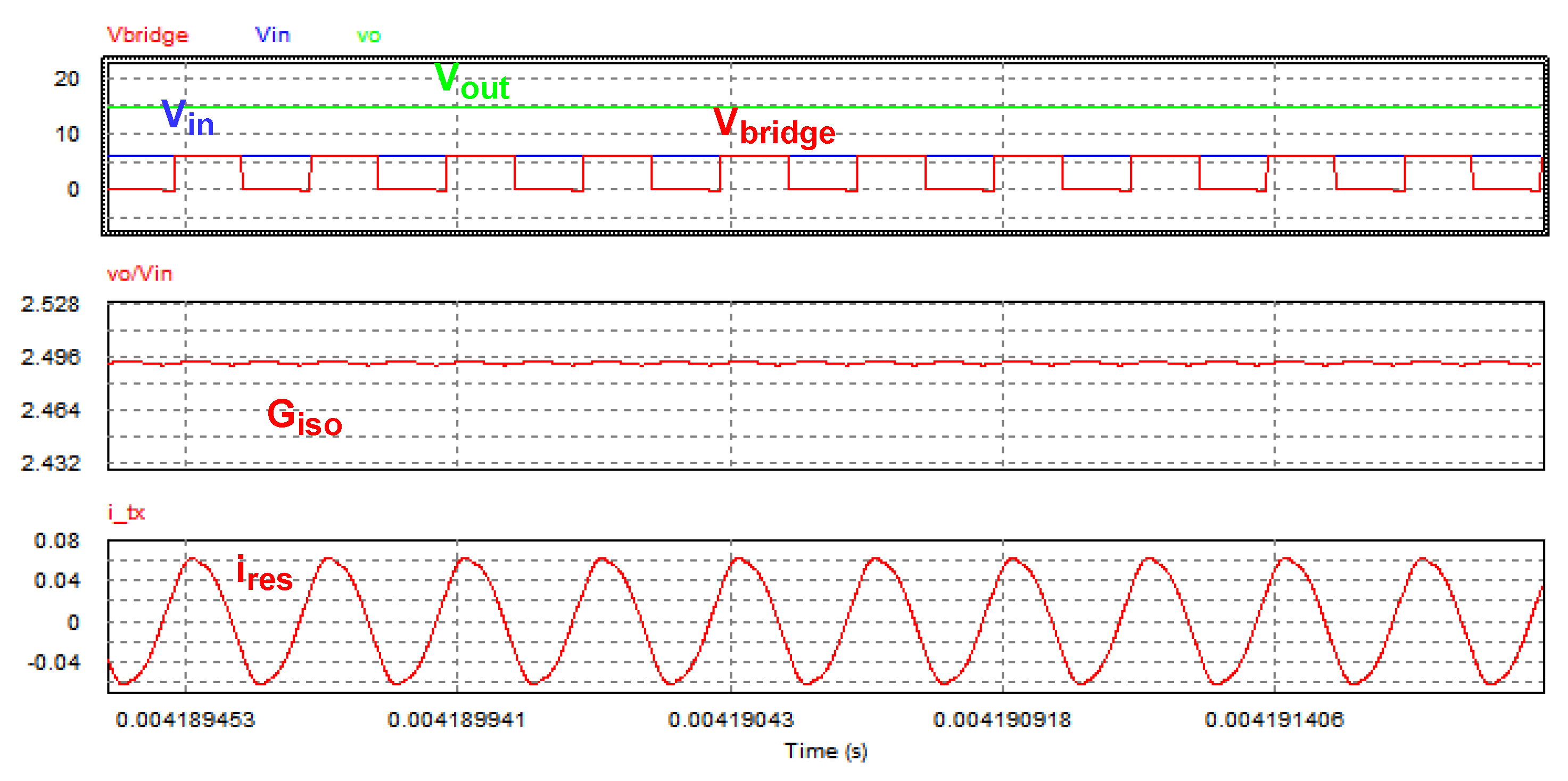
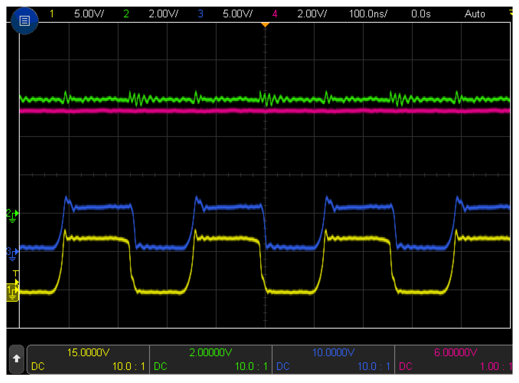
4.2. Prototype Measurements

Using the procedure described in Section 4.1, an analog isolator was constructed. It was designed to have a G i s o = 2.5 using a switching frequency f s = 4 MHz.
The schematic of Figure 4a was implemented as a prototype to verify the behavior of the system. Following the necessity of using space qualified components (preferably from [7]), all the NPN transistors are 2N2222 and the PNP are 2N2907 and the diodes are 1N4148. The oscillator is built using a CD4093B CMOS NAND gate array, which features four gates and the op-amp is the LT6020 from Analog Devices, which has a space grade counterpart.
The transformer was implemented using a small iron powder toroidal core from Micrometals. The size is a T37 and the material is the −8. These magnetic cores are usually used implementing transformers and inductors for RF and power conversion applications. With this material, the permeability variation against frequency is negligible up to 20 MHz. The toroidal shape implies that the only way for adjusting L m is the number of turns and in order to adjust L l k 1 and L l k 2 the separation of the windings shall be controlled. In the design, L m = 14 μ H and L l k 1 = L l k 2 = 8.8 μ H, which are very close with the values simulated with ANSYS PEmag. Note how similar that L m is to L l k 1 . This is the reason behind the analysis performed in Section 3.1.2. The parasitic resistances considered are r p 1 = 1.12 Ω and r p 2 = 1.12 Ω . Having the winding separated also contributes to minimizing the parasitic capacitance between the primary and the secondary of the transformer. No other stray capacitances were considered since the ones to the enclosure will greatly depend on the final implementation.
The goal would be to have a gain G t a n k = 5.0 . The design procedure leads to having C t a n k = 68 pF and R l = 2.2 k Ω . The output capacitor C o = 22 nF. It is important to remark that the current through C t a n k will have a frequency of 4 MHz, so high frequency RF capacitors shall be used since normal ceramic ones will have a very high ESR. With this design, gain G t a n k should be 5 and therefore G i s o = 2.5 .
The prototype is supplied with V D D = 15 V. The main waveforms of the analog isolator can be seen in Figure 10. The isolator is tasked there to track voltage V i n , which is a DC voltage of 6 V (depicted in green). The oscillator output waveforms (depicted in yellow), which should be 15 V amplitude, are clamped to 7 V, which is the V s u p _ b r i d g e voltage plus the voltage drop in the diode. This avoids BJT saturation. It can be appreciated how V b r i d g e (depicted in blue) rises before the oscillator indicating ZVS behavior in the bridge. It can be seen how the isolator provides a gain having an output voltage of V o u t = 9.54 V (depicted in purple). Thus, having a gain of G i s o = 1.59 , which according to (15) would mean that G t a n k = 3.18 , way below the target value of G t a n k = 5 . However, the expression of (11) is for a perfectly square waveform between 0 and V i n . In Figure 10, it can be seen how the minimum value of V b r i d g e is around 0.7 V. This is coincident with the fact that the saturation voltage of the BJTS is around 0.7 V. Moreover, (11) is for a duty cycle of D = 0.5 ; in the waveforms, it is around D = 0.55 . Then, the first harmonic of the voltage is smaller than the one calculated by (11). Re-evaluating G t a n k using (16) with the amplitude and duty cycle measured with the oscilloscope for V b r i d g e (then having V i n = V b r i d g e _ m a x V b r i d g e _ m i n ), the value obtained is G t a n k = 4.88 , which is much closer to the theoretical value.
As this isolator is designed to track varying voltages and to integrate it in control loops, it is necessary to measure the transfer function between V i n and V o u t using a network analyzer around the DC point of 6 V. The frequency range was between 10 Hz and 1 MHz. Results can be seen in Figure 11. It can be seen how the gain is flat up to 20 kHz having a small signal gain at 10 Hz of G i s o _ s s = 4.6 dB, which in natural units is G i s o _ s s = 1.69 , very close to the static gain measured G i s o = 1.59 . This frequency behavior has to be taken into account for integrating the analog isolator in a control loop such as in Figure 4b.
The Bode plot of Figure 11 was used to tune the current control loop of an LCL based on an N channel SiC MOSFET. The circuit for the LCL (depicted in Figure 2b) with the current sensor, the controller, and the analog isolator were simulated in LTSPICE. Figure 12 shows the result of the simulation. It can be seen how the measured current is below the reference. After a faulty overload, the control loop reacts lowering the gate to source voltage. This makes the MOSFET operate as a current source and then it limits the current demanded by the load. It can be seen how the measured current follows the reference value in a smooth way without any oscillation. This verifies the applicability of the analog isolator design for driving the gate of a MOSFET operating as a current source.

5. Conclusions

The present paper shows a design of an analog isolator capable of being integrated in power applications. As its design uses discrete rad-hard components, it can be used in space applications. The design procedure is flexible enough so it can be tailored for specific applications. The static gain can be adjusted by means of adjusting the resonant tank but margins for taking into account the saturation voltage of BJTs and other non-idealities shall be considered. No power is necessary for the secondary part of the isolator making it adequate for driving the gate of an N channel MOSFET in linear mode thus controlling a Latching current limiter.
As desired, the bandwidth is quite high, making it capable of complying in simulation with the requirements of the Latching current limiters which was the target application. Nonetheless, it can be used for other applications in which a measurement of an isolated voltage is needed.
The proposed design is based on an LLC converter. However, other DC/DC converters can be used for the same application based on the principle of changing the input voltage. The LLC allows for adjusting the gain, but it is a complicated design. For other applications, other topologies can be used. One of the drawbacks is that it can only measure a positive voltage. Some modifications will be needed for negative ones.
The design also shows one of the characteristics of space applications. As the devices shall be rad-hard, the availability is much scarce. For the present design, it meant going for a fully discrete implementation. The switching devices (BJTs) are probably not the best option. For a terrestrial application (provided that some of the characteristics of the presented magnetic isolator were desired), it would have been better to use P and N MOSFETS driven by logic levels. Even better, it would have been to use a high current high speed inverter or a high speed MOSFET driver as the Renesas EL7156 as the switching half-bridge. However, to the best knowledge of the authors, such devices are not available as space grade components.
The use of a discrete approach has also one advantage. It is easier to investigate the effect of failures in the individual components rather than in an integrated circuit. These are the analysis known as Failure Mode Effect and Criticality Analysis (FMECA) which are required for any space application.
In summary, the paper presents an analog isolator design compatible with space power application that can be tailored to specific requirements regarding isolation, gain, and bandwidth.

Author Contributions

All the authors contributed to the Writing—original P.F.M. and M.A. performed the Conceptualization, Supervision and Funding acquisition and A.L. contributed to the Investigation. All authors have read and agreed to the published version of the manuscript.

Funding

This research work was partially funded by the Spanish Ministry of Science, Universities and Innovation through the grant MCIU-19-RTI2018-099682-A-I00 and through the Small TRP program (ESA-TRP-TEC-SOW-012881) by the European Space Agency (ESA).

Conflicts of Interest

The authors declare no conflict of interest. The funders had no role in the design of the study; in the collection, analyses, or interpretation of data; in the writing of the manuscript, or in the decision to publish the results.

References

  1. Reed, R.A.; Poivey, C.; Marshall, P.W.; LaBel, K.A.; Marshall, C.J.; Kniffin, S.; Barth, J.L.; Seidleck, C. Assessing the impact of the space radiation environment on parametric degradation and single-event transients in optocouplers. IEEE Trans. Nucl. Sci. 2001, 48, 2202–2209. [Google Scholar] [CrossRef]
  2. LaBel, K.A.; Kniffin, S.D.; Reed, R.A.; Kim, H.S.; Wert, J.L.; Oberg, D.L.; Normand, E.; Johnston, A.H.; Lum, G.K.; Koga, R.; et al. A compendium of recent optocoupler radiation test data. In Proceedings of the 2000 IEEE Radiation Effects Data Workshop, Workshop Record, Held in conjunction with IEEE Nuclear and Space Radiation Effects Conference (Cat. No.00TH8527), Reno, NV, USA, 24–28 July 2000; pp. 123–146. [Google Scholar]
  3. Microsemi. SA50-120-12S-B-P Rad Hard DC/DC Converter Datasheet. Available online: https://www.microsemi.com/document-portal/doc_view/134142-sb30-28-datasheet (accessed on 28 July 2020).
  4. U-94 The UC1901 Simplifies the Problem of Isolated Feedback in Switching Regulators; Technical Report; Unitrode: Merrimack, NH, USA, 1999.
  5. Irving, B.T.; Jovanovic, M.M. Analysis and Design Optimization of Magnetic-Feedback Control Using Amplitude Modulation. IEEE Trans. Power Electron. 2009, 24, 426–433. [Google Scholar] [CrossRef]
  6. Sayani, M.; White, R.; Nason, D.; Taylor, W. Isolated feedback for offline switching power supplies with primary-side control. In Proceedings of the APEC ’88 Third Annual IEEE Applied Power Electronics Conference and Exposition, New Orleans, LA, USA, 1–5 February 1988; pp. 203–211. [Google Scholar] [CrossRef]
  7. European Preferred Parts List ESCCC/RP/EPPL007-38. 2019. Available online: https://escies.org/download/webDocumentFile?id=67263 (accessed on 28 July 2020).
  8. Texas Instruments. UC1901 Datasheet; Texas Instruments: Dallas, TX, USA, 2010. [Google Scholar]
  9. Analog Devices. ADuM3190S Datasheet; Analog Devices: Norwood, MA, USA, 2019. [Google Scholar]
  10. Space Engineering-Electrical Design and Interface Requirements for Power Supply; ECSS: Noordwijk, The Netherlands, 2016.
  11. Space Engineering-Guidelines for Electrical Design and Interface Requirements for Power Supply; ECSS: Noordwijk, The Netherlands, 2016.
  12. Space Product Assurance—Derating—EEE Components; ECSS: Noordwijk, The Netherlands, 2011.
  13. De Simone, S.; Adragna, C.; Spini, C.; Gattavari, G. Design-oriented steady-state analysis of LLC resonant converters based on FHA. In Proceedings of the International Symposium on Power Electronics, Electrical Drives, Automation and Motion, SPEEDAM, Taormina, Italy, 23–26 May 2006; pp. 200–207. [Google Scholar] [CrossRef]
  14. Simone, S.D. LLC Resonant Half-Bridge Converter Design Guideline; STMicroelectronics: Coppell, TX, USA, 2007. [Google Scholar]
  15. Abdel-Rahman, S. Resonant LLC Converter: Operation and Design; Infineon: Neubiberg, Germany, 2012. [Google Scholar]
  16. Park, H.P.; Jung, J.H. Power Stage and Feedback Loop Design for LLC Resonant Converter in High-Switching-Frequency Operation. IEEE Trans. Power Electron. 2017, 32, 7770–7782. [Google Scholar] [CrossRef]
  17. Steigerwald, R. A Comparison of Half-Bridge Resonant Converter Topologies. IEEE Trans. Power Electron. 1988, 3, 174–182. [Google Scholar] [CrossRef]
Figure 1. Analog Isolator concept.
Energies 13 04504 g001
Figure 2. Latching Current Limiters: (a) P Channel based; (b) N Channel based.
Energies 13 04504 g002
Figure 3. Analog Isolator Schematic.
Energies 13 04504 g003
Figure 4. Analog Isolator options: (a) Implementation with op-amp; (b) Integration with control loop.
Energies 13 04504 g004
Figure 5. Oscillator and transformer driver.
Energies 13 04504 g005
Figure 6. Network for first harmonic analysis.
Energies 13 04504 g006
Figure 7. Equivalent network for FHA.
Energies 13 04504 g007
Figure 8. Gain of the resonant network: (a) With Q t a n k = 0.2 ; (b) With Q t a n k = 1 .
Energies 13 04504 g008
Figure 9. PSIM simulation results.
Energies 13 04504 g009
Figure 10. Waveforms of the isolator.
Energies 13 04504 g010
Figure 11. Bode plot of the gain of the Analog Isolator.
Energies 13 04504 g011
Figure 12. LTSPICE simulation results of the LCL.
Energies 13 04504 g012

