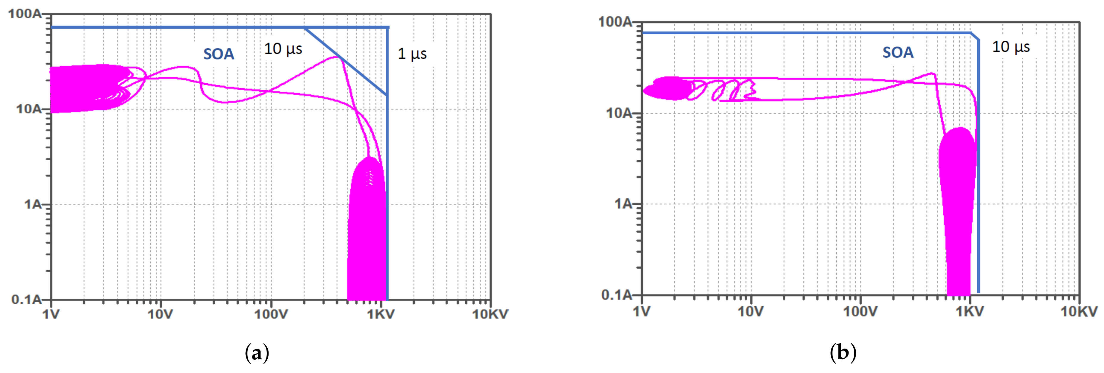
Both LTspice and PLECS were used for the simulation analysis, as explained in
Section 4.3. The device characterization in terms of conduction and switching losses has been done by double pulse tests on real device models in LTspice. In the next step, these losses connected to the different operating conditions were inserted in the look-up tables in PLECS and in this way it was possible to characterize each device for each switching period. The three-leg interleaved dc–dc converter (as shown in
Figure 1) was implemented in PLECS. For the efficiency analysis the simpler converter model was considered, i.e., without the parasitics, as usually they can be neglected and are the same for the two converters. As resulted from the parasitics analysis, the external gate resistance of 0
was used for double pulse test in the case of SiC-MOSFET device, considering only the internal resistance of the gate driver, i.e., 1.5
. Instead, for the Si-IGBT device the external gate resistance of 3.5
was used. The other simulation parameters are listed in
Table 4. The
–
pairs for each converter have been defined in
Table 3 and were used here for simulations of different cases. The specific
–
pairs were selected in order to keep the output current ripple within 5%. Cases with different output currents of 30, 45, 60 and 75 A were analyzed, corresponding to the 25%, 50%, 75% and 100% of the output power. The control reference was compared with three shifted carriers in order to obtain the pulse-width modulation (as explained in
Section 2), providing a fixed switching frequency.
5.1. Inductor Selection
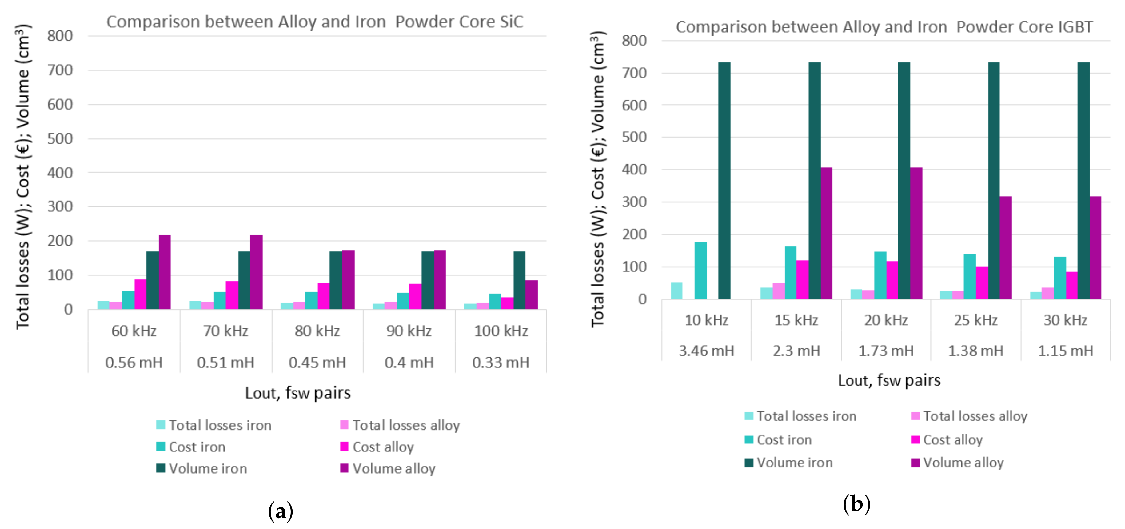
The comparison of different core types given in
Table 5 has been shown in
Figure 5, for the two core types found as the best compromise for the total inductor losses and inductor volume. Two different types have been considered for both converters, iron (in turquoise) and alloy (in pink) powder core from [
31]. In
Figure 5 is given the comparison of total core losses, costs (obtained from the core manufacturer) and volume for the case of 25 A inductor current corresponding to the 75 A output current. In the case of SiC-MOSFET the difference between the volume of iron and alloy inductors is not very marked, except in the case of the highest switching frequency (0.33 mH–100 kHz) where the alloy core allows one to have an inductor with volume reduced to half (171 cm
–85.5 cm
).
For Si-IGBT-based converter there was more significant difference in the volume of iron and alloy core except for the 3.46 mH–10 kHz pair, where it was not possible to design the alloy powder core. When considering the lowest (10 kHz) and highest (30 kHz) switching frequencies, the alloy allowed 57% reduction in core volume.
Evident also are the reductions in volume, losses and costs in both iron and alloy powder core when comparing
Figure 5a,b for SiC-MOSFET-based converter, confirming the advantages of using the SiC-MOSFET devices. For the two highest switching frequencies (30 kHz for Si-IGBT and 100 kHz for SiC-MOSFET), the SiC-MOSFET-based converter can offer the reduction of 73% of the core volume for alloy core, and 77% for the iron core, having around 60% lower cost.
In this case, the best compromise in terms of total losses and volume has been taken into account. The selected inductors are given in bold in
Table 5. In some cases the best choice is iron core, while in other cases it is alloy core. For the SiC-MOSFET-based converter the best solutions are almost always in iron, except for the case with the highest switching frequency (100 kHz), which also represents a significant working condition, allowing one to make the most of the advantages offered by SiC-MOSFET devices and significantly reduce weight and volume. On the other hand, for Si-IGBT the best solutions are always in alloy, except for the lowest switching frequency (10 kHz) with only possible solution in iron. However, this working condition is not very significant because it leads to higher volume and cost. Further on in the analysis, only the inductors given in bold were considered for the efficiency comparisons.
5.2. Power Loss and Efficiency Comparisons
In this section the power loss and efficiency comparison is presented. The three-leg interleaved dc–dc converter supplying a resistive load and implemented in PLECS has been used for this purpose. For each specific value of
the inductance with its winding resistance (as resulted from the inductor design shown in
Table 6) has been used for the modeling. The converter losses have been determined directly from the PLECS simulation tool, while the inductor losses (for each specific inductor designed) have been calculated as described in
Section 4.2.
In
Figure 6 are given the dc–dc converter losses in the case of different output inductor–switching frequency pairs and output currents in the case of 50
C heat sink temperature. In particular, four values of the output current have been considered: 30, 45, 60 and 75 A. The two converters show rather similar losses, even though the SiC-MOSFET converter’s switching frequency is much higher than the one of Si-IGBT converter (60–100 kHz vs. 10–30 kHz). For the highest output current of 75 A, the SiC-MOSFET-based converter has 28%, 18% or 9% higher losses when compared to Si-IGBT-based converter for the switching frequencies below 80 kHz (for Si-IGBT below 20 kHz) respectively, but lower 1% for the 90kHz and 9% for 100 kHz, as shown in
Figure 7a. Generally, all the losses show the same behavior, lower in case of Si-IGBT for the switching frequencies <20 kHz. More flat behavior of the losses for SiC-MOSFET-based converter can be noted, i.e., less variations with the change of
–
pairs for the specific current.
In
Figure 8 are given the total inductor losses for the selected inductors from
Section 5.1. In particular, they resulted from the sum of inductor core and winding losses in the case of different inductors and output currents, as for converter losses. Different inductors have been designed, as shown in
Table 6. The criteria for the design were the lowest total inductor losses, but also the lowest volume. The standard design practice has been applied; for example, the difference of the unloaded and loaded unductor was set to 10%, the cross section of the winding was carefully selected taking into account the minimum banding radius of the wire, the filling of the core window area was set to less than 50%, etc.
From the
Table 6 can be noted 3.7 times lower inductor volume when comparing the cases with highest switching frequencies in the case of SiC-MOSFET-based converter. In
Figure 8 the maximum losses for SiC-MOSFET-based converter of 24.9 W can be seen for the 0.56 mH–60 kHz pair and 75 A output current, while for the Si-IGBT-based converter the maximum is for 3.46 mH–10 kHz pair reaching 52.6 W at 75 A output current. The minimum losses for SiC-MOSFET-based converter are for 0.4 mH–90 kHz with 6.9 W in the case of lowest output current, while for Si-IGBT-based converter the minimum losses of 10.7 W are for 1.38 mH–25 kHz pair and the same value of the output current. In
Figure 7b are given the inductor losses for the highest output current, i.e., 75 A. The losses of SiC-MOSFET-based converter are lower for all
–
pairs, with the highest difference of 53% at the lowest switching frequency. Conveniently, the total one-leg losses are also depicted in
Figure 7c, obtained as the sum of device losses and inductor losses per leg at 75 A output current. It is interesting to see that the Si-IGBT-based converter has higher losses in almost all cases, except the 1.73 mH–20 kHz case, where SiC-MOSFET-based converter shows 4% higher losses.
For the particular case in
Figure 7c, where SiC-MOSFET-based converter shows slightly higher losses, the loss distribution has been analyzed for all the values of the output current. In
Figure 9 is shown the distribution of the total losses (simulated device and analytical inductor) of one converter leg, and specifically for the 0.45 mH–80 kHz pair (SiC-MOSFET-based converter) and the 1.73 mH–20 kHz pair (Si-IGBT-based converter) in the case of 50
C heat sink temperature. The figure also gives the comparison with the theoretical values, calculated as explained in
Section 4.1 and
Section 4.2.
The total losses of SiC-MOSFET-based converter (dark pink) are higher only in the case of 75 A output current, as resulted also in
Figure 7c, while for the other current values it shows lower losses compared to Si-IGBT converter (dark green). As for the losses of the devices in one converter leg, the switching losses which are also shown in the figure are slightly lower for the SiC-MOSFET-based converter, even though the switching frequency was four times higher. The total inductor loss (dotted traces) is slightly lower for SiC-MOSFET-based converter, having core losses invariant with the change of the output current, as expected. For the specific case of 75 A output current, the SiC-MOSFET-based converter shows elevated conduction losses, and this is the reason why it resulted in higher total losses. Moreover, also the good agreement between simulation results (first bar) and analytical results (second bar) for all cases can be observed.
In
Figure 10 are shown the total three-leg losses of the two converters, including the inductor losses resulting from realistic simulations (for power switches), and analytical for the different inductors. Generally, the SiC-MOSFET-based converter showed lower total losses (in pink), especially for the lower output currents. The highest losses can be noted for the Si-IGBT-based converter and 1.15 mH–30 kHz pair for all the values of the output current, due to high devices’ losses. While the SiC-MOSFET-based converter has more uniform losses behavior with the change of switching frequency, this difference is more outlined in the Si-IGBT-based converter.
In
Figure 11 are shown the efficiencies of the two three-leg converters for different
–
pairs and output currents. For both converters, the efficiency is rather high, higher in the case of lower switching frequencies due to lower losses. The SiC-MOSFET-based converter shows higher efficiency (ranging between 98.3% and 98.9%), while in the case of Si-IGBT the efficiency ranges from 98% to 99%. The efficiency curves are closer to each other in the SiC-MOSFET when compared to Si-IGBT case, meaning that in the SiC-MOSFET case there is a lower variability of efficiency with the change of
–
pairs. In the worst case (30 A) there is a variability of about 0.3% in the case of SiC-MOSFET and 0.7% in the case of Si-IGBT. Therefore it can be concluded that by adopting the SiC-MOSFET solution, efficiency depends less on the choice of switching frequency and inductor.
5.3. Heat Sink Volume
In order to conduct a throughout comparison of the two converters, the heat sink volume and cost should also be taken into account. The heat sink volume analysis was based on the power loss of the two converters at highest output current (75 A) and considering 50
C heat sink temperature. In order to evaluate the heat sink volume, it is necessary to calculate the thermal resistance of the heat sink:
where
is the heat sink temperature,
is the ambient temperature and
is the total converter loss.
Once the
is calculated, it is possible to obtain the heat sink volume based on natural air convection [
33]. The minimum heat sink volume can be obtained from the fitting function:
where
is expressed in cm
and
in
. Equation (
17) in [
33] has the results of the curve fitting of various extruded naturally cooled heat sinks against heat sink thermal resistance.
Heat sink volume calculated from the curve fitting function for the two converters is presented in
Figure 12, starting from the lowest switching frequency considered for both converters. A room temperature of 25
C was selected as ambient temperature. The results show that the SiC-MOSFET-based converter has an increase of around 3% only in the case of 0.45 mH–80 kHz pair. In the other cases, the Si-IGBT-based converter has higher heat sink volume, with the highest difference of 7% in the case of highest switching frequency.
5.4. Cost Comparison
This section presents the cost comparison of the two interleaved dc–dc converters, taking into account only the costs that are different for the two converters, i.e., the switching device costs, the heat sink costs and the inductor costs. The same cost was considered for the other components (for example gate driver, power cables, etc.), and therefore was not included in this comparison.
In
Figure 13 is shown the comparison of the converter efficiency (3-legs, including inductors), the total volume (heat sink and inductor, in dm
) and total converter cost (in € per kW). For the efficiency comparison, the power switch losses were taken directly from the realistic circuit model implemented in PLECS, while for the different inductors they were calculated analytically. Note that the costs in
Figure 13 refer to the sample prices of the main parts’ manufacturers in Europe. Having in mind that the price of SiC-MOSFET devices is 2–3 times the price of IGBT devices, and the costs of different inductors for the SiC-MOSFET-based converter generally being lower (due to lower volume), the goal of this analysis was to verify if the difference of the device cost can somehow be compensated with the lower inductor cost. Namely,
Figure 13 confirms this fact, where the SiC-MOSFET-based converter shows lower total cost for all the
–
pairs. The trend of the cost curve for the SiC-MOSFET-based converter is almost flat, with the lowest cost for the highest switching frequency, i.e., 100 kHz. The Si-IGBT-based converter shows more cost variation, with the lowest cost for the highest switching frequency as well. For the higher switching frequencies, the two costs are practically the same for each device.
The total volume and efficiency confirm the advantage of using the SiC-MOSFET-based converter. The efficiency is almost always higher or equal to the one of the Si-IGBT-based converter. The only case in which the Si-IGBT-based converter showed higher efficiency was for 1.73 mH–20 kHz pair. The trend of the SiC-MOSFET efficiency curve is more flat, while the Si-IGBT-based converter shows higher variations with the lowest efficiency for 30 kHz switching frequency.
The real benefit can be seen in the total volume, where the lower volume can be noted for all the
–
pairs in the SiC-MOSFET-based converter. For the highest switching frequency, SiC-MOSFET-based converter offers the lowest total volume. Generally,
Figure 13 leads to the conclusion that the best working conditions for Si-IGBT-based converter could be medium switching frequencies (20 kHz and 25 kHz), where the cost, volume and efficiency differences are less marked, while the worst working conditions are the lowest switching frequencies, with elevated cost and volume difference. On the other hand, the real advantage of the SiC-MOSFET-based converter can be seen at high switching frequencies, where the cost is practically the same for the two converters (and lowest for all cases), efficiency remains higher and total volume is lower.
These considerations, together with the fact that the prices for SiC-MOSFET devices tend to reduce greatly over ther years, indicate the convenience of using SiC-MOSFET devices, especially given the fact that it offers lower total volume.

 ,
, 


