Article

Carrier Transmission Mechanism-Based Analysis of Front Surface Field Effects on Simplified Industrially Feasible Interdigitated Back Contact Solar Cells

1
School of Microelectronics, Dalian University of Technology, Dalian 116024, China
2
School of Physics, Dalian University of Technology, Dalian 116024, China
*
Author to whom correspondence should be addressed.
Energies 2020, 13(20), 5303; https://doi.org/10.3390/en13205303
Submission received: 30 September 2020 / Revised: 7 October 2020 / Accepted: 8 October 2020 / Published: 12 October 2020
(This article belongs to the Section D1: Advanced Energy Materials)

Abstract

:
Interdigitated back contact (IBC) n-type silicon solar cells with a different front surface layer doping concentration were fabricated and studied and the influence of the front surface doping level was analyzed via simulation (PC1D). The IBC cells were processed by industrially feasible technologies including laser ablation and screen printing; photolithography was not used. A maximum efficiency of up to 20.88% was achieved at an optimal front surface field (FSF) peak doping concentration of 4.8 × 1019 cm−3 with a sheet resistance of approximately 95 Ω/square, corresponding to Jsc = 40.05 mA/cm2, Voc = 671 mV and a fill factor of 77.70%. The effects of the front surface doping level were studied in detail by analyzing parameters related to carrier transmission mechanisms such as minority carrier concentration, minority carrier lifetime and the saturation current density of the FSF (J0e). The influence of the front surface recombination velocity (FSRV) on the performance of IBC solar cells with different FSF layer doping concentrations was also investigated and was verified by examining the variation in the minority carrier density as a function of the distance from the front surface. In particular, the impact of the FSF doping concentration on the Jsc of the IBC cells was clarified by considering carrier transmission mechanisms and the charge-collection probability. The trends revealed in the simulations agreed with the corresponding experimental data obtained from the fabricated IBC solar cells. This study not only verifies that the presented simulation is a reasonable and reliable guide for choosing the optimal front surface doping concentration in industrial IBC solar cells but also provides a deeper physical understanding of the impact that front surface layer doping has on the IBC solar cell performance considering carrier transmission mechanisms and the charge-collection probability.

Graphical Abstract

1. Introduction

Interdigitated back contact (IBC) n-type solar cells [1,2] have attracted much attention in recent years. Their high efficiency reduces the manufacturing cost by increasing the amount of electric power generated by each photovoltaic (PV) system [3,4,5]. The high efficiency can be attributed to the remarkable optoelectrical properties. When compared with the front contact cells, the first and most important advantage of the IBC solar cells is the complete elimination of optical shading toward the front side. This can be achieved by transferring the metal grids to the rear surface, which is typically responsible for increasing the short-circuit current density by 4–8% [6,7]. Second, avoiding the front surface metal contacts reduces the series resistance because it allows a large proportion of the rear surface to be metallized, resulting in a high fill factor (FF). Third, the optimization of the front surfaces of IBC cells is more flexible, both in terms of passivation and optical performance, when there is no tradeoff between the low contact resistance and low recombination associated with the front contact cells. In addition, the IBC solar cells not only exhibit aesthetic externals but also simplify the module assembly because of the all-back-side electrode design [8], improving the throughput rate and reducing the production cost. Franklin et al. reported IBC solar cells (lab-scale design of 2 × 2 cm2) with an efficiency of 24.4% fabricated via photolithography and aluminum evaporation [7]. Chen et al. investigated three novel designs to passivate IBC solar cells using SiO2/SiNx:H and Al2O3/SiNx:H [9]. Hollemann et al. achieved an IBC cell efficiency of 26.1% with a 1.3 Ω⋅cm p-type float zone (FZ) wafer featuring a polycrystalline silicon on oxide (SiOz) junction [10]. Heterojunctions were combined with the IBC solar cells to achieve high conversion efficiencies [11,12,13]. However, almost all of the reported high efficiency IBC cells were fabricated via complex, expensive and time-consuming processes such as photolithography, physical evaporation and electroplating. To reduce the production costs, the IBC cell structure must be optimized and the IBC cell fabrication process must be simplified.
Numerical simulation is a crucial complementary tool to experimental work as it is cost-effective and time-saving. It is not only convenient for the optimization of cell design by modifying different parameters in the simulation software but it also provides an in-depth understanding of cell operating mechanisms. PC1D is the most widely used solar cell modeling program and has proved to be efficient and reliable in the literature [14,15,16,17,18,19,20,21,22]. In this work, the effect front surface layer doping concentration has on IBC cell performance is systematically investigated by using both simulation and experimental measurement. PC1Dmod Ver.6.2 is initially applied to investigate IBC cell operating principles with various front surface doping concentrations as a function of front surface recombination velocity (FSRV). The cell performance, especially the short-circuit current density and dependence on the front surface layer doping concentration are analyzed by considering the carrier transmission mechanisms and charge-collection probability, thus verifying the simulated results. By comparing the characteristic parameters of measured current-density voltage (J-V) curves including short-circuit current density (Jsc) and open-circuit voltage (Voc), the optimal front surface layer doping concentration is determined. Based on the simulation results, industrially feasible photolithography-free IBC solar cells are fabricated in a commercial pilot line of the passivated emitter and rear cell (PERC) using laser ablation and screen printing; different front surface layer doping concentrations are applied to the fabricated cells and the influence of the doping concentration on the IBC solar cell performance is investigated. To further reduce the production cost of IBC cells, a novel method using screen printed phosphorus paste is applied to form a back surface field (BSF). The presented novel, simplified process in combination with the optimal front surface doping concentration of 4.8 × 1019 cm−3 results in an efficiency of up to 20.88%. The trends associated with the experimental results agree with those associated with the simulation data, indicating the validity and reliability of the simulation results and corresponding analysis.

2. Materials and Methods

2.1. Simulation Methods

PC1D software is used to carry out in-depth investigations of the physical mechanisms behind how different front surface doping concentrations influence cell performance. Initially released in 1985 [23], PC1D was further developed into multiple versions, becoming the most widely used simulation program in the solar cell community; it is open source and uses the finite-element method to simulate semiconductor device characteristics.
A modified version of PC1D released by Halvard Haug and Johannes Greulich from the Institute for Energy Technology in Norway and the Fraunhofer Institute for Solar Energy Systems in Germany, respectively [22], PC1Dmod Version 6.2 (current version as of this writing), is used in this study. The principles of PC1Dmod Version 6.2 are introduced briefly to provide the foundation for the numerical simulation calculation. The relative parameters describing the crystalline Si solar cells are abstracted in PC1D by solving physical equations [24].
  J n   =   μ n   n E Fn
  J p   =   μ p   p E Fp
Equations (1) and (2) reveal the carrier transport behaviors in silicon, representing the electron ( J n ) and hole ( J p ) current densities in terms of the electron ( μ n ) and hole ( μ p ) mobilities, the electron (n) and hole (p) densities and the electron ( E Fn ) and hole ( E Fp ) quasi-Fermi energies.
n =   N c   F 1 / 2 q ψ + V n q ϕ n , i + ln n i , 0 N c k B T
p =   N v   F 1 / 2 q ψ + V p + q ϕ p , i + ln n i , 0 N v k B T
By substituting the charge carrier statistics Equations (3) and (4) into Equations (1) and (2), respectively, n and p are eliminated, thus simplifying the calculation. Here, N c and N v represent the conduction- and valence-band effective density of states, respectively. F 1 / 2 is the full Fermi–Dirac integral of order 1 / 2 Equations (3) and (4) are also influenced by the band-edge potentials ( V n , V p ), quasi-Fermi potentials ( ϕ n , i , ϕ p , i ), intrinsic carrier concentration ( n i , 0 ), Boltzmann constant ( k B ) and temperature ( T ).
n t   =   J n q   +   G L U n
p t   =   J p q   +   G L U p
Equations (5) and (6) are continuity equations describing the behavior of all electrons and holes entering a given volume of space.   G L is the volume generation rate of electrons or holes due to the absorption of light (photogeneration).   U n and U p denote the net recombination rate of electrons and holes, respectively. Note that in the two-carrier model, electrons and holes are always generated and annihilated in pairs. Therefore, U n is equal to U p .
2 ψ = q ε   n p + N A N D +
Poisson’s equation of electrostatics is given by Equation (7) where ψ is electrostatic potential and ε is permittivity. The total charge density n p + N A N D + in Equation (7) comprises four parts including the electron density n , the hole density p , ionized donor density ( N D + ) and ionized acceptors density N A . Based on Equations (3) and (4), five unknown parameters, including electrostatic potential ( ψ ) , quasi-Fermi energies ( E Fn , E Fp ) and current densities ( J n , J p ), are present in five fundamental equations. Therefore, with the appropriate boundary conditions, the simulation obtains solutions for a given structure of a crystalline silicon solar cell. The corresponding simulation parameters are presented in Table 1.

2.2. Experimental Methods

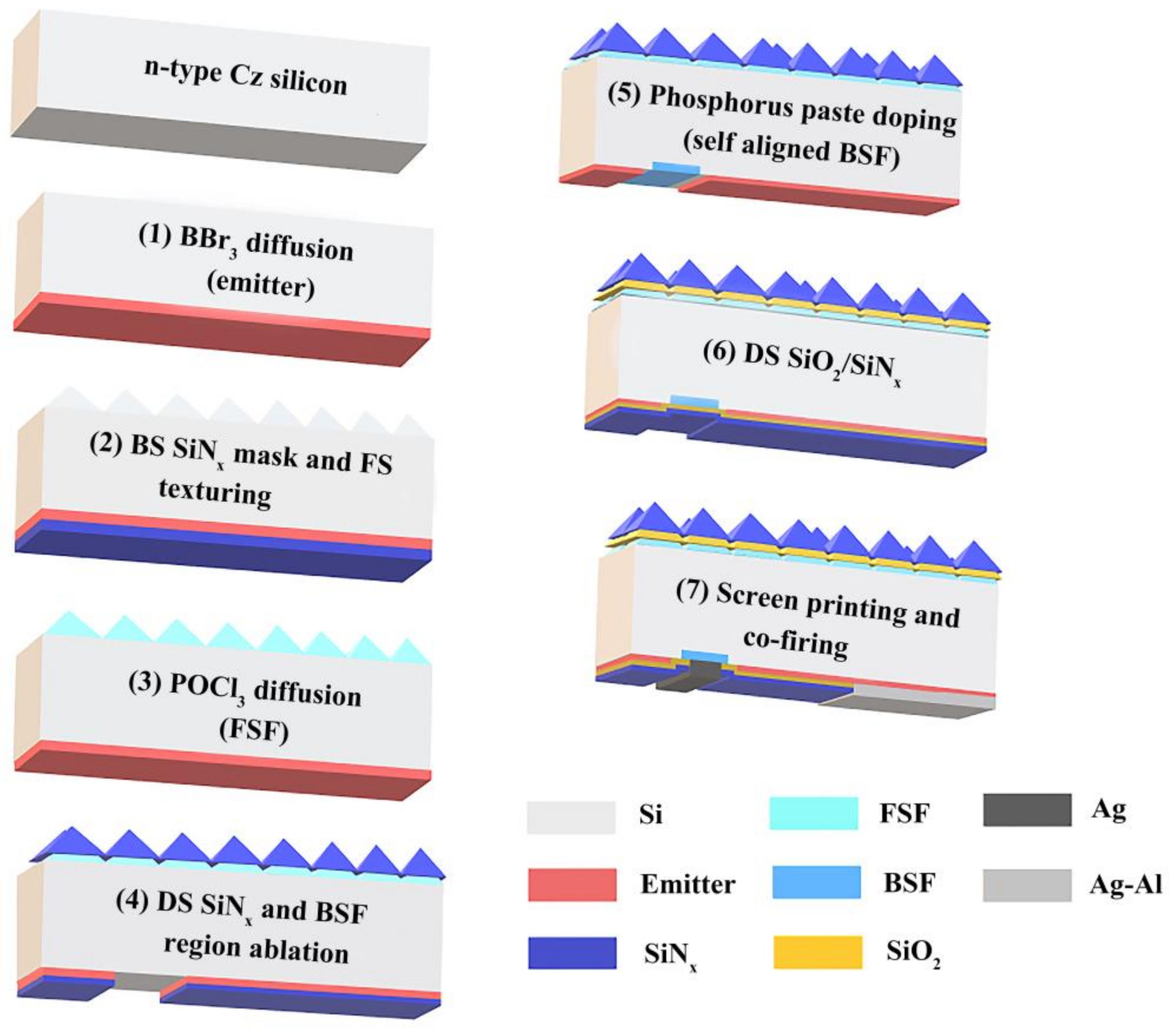
A schematic showing a cross section of the fabricated and analyzed industrially viable n-type IBC Si solar cell is presented in Figure 1. All of the samples were prepared in accordance with a novel and simplified industrially feasible process shown in Figure 2.
In the present study, all of the solar cells (2 × 2 cm2) were prepared using double-side polished Czochralski (Cz) n-type Si wafers with a resistivity of 1–4 Ω cm and a thickness of 180 μm, which were then subjected to RCA cleaning. BBr3 diffusion was then applied to obtain the emitter on the back side (BS) of the wafer (step 1, p+ emitter formation). The wafers were subsequently dipped etch in HF solution, whereas plasma-enhanced chemical vapor deposition (PECVD) was used to deposit a BS SiNx layer (approximately 100 nm thick) to protect the emitter, texturing only the front side (FS) (step 2, BS SiNx mask and FS texturing). After texturing and cleaning, POCl3 diffusion was performed to form a front surface doping layer, i.e., n+ FSF (step 3, n+ FSF formation). Next, SiNx with a thickness of 80 nm was deposited on the double side (DS) and the opening of the BSF was obtained at the rear side via laser ablation (step 4, DS SiNx and BSF region ablation). Afterward, BSF diffusion was achieved using self-aligned phosphorus paste screen printing followed by a thermal drive-in (step 5, self-aligned BSF). The phosphorus silicate glass (PSG) was then removed and DS oxidation with a thickness of approximately 10 nm was achieved at 850 °C in O2. Considering the SiO2 thickness, 70 nm SiNx layers were deposited on the DS via PECVD and the SiNx layer served as an antireflective and passivation coating for the FS. Moreover, the PECVD SiNx layer on the BS acted as an enhanced internal rear reflectance and rear passivation coating (step 6, DS SiO2/SiNx). Finally, the self-aligned screen printing of metal paste was used to create the BS contacts (step 7, screen printing and co-firing). To prepare the reference samples, the same process was followed except for the POCl3 diffusion step at the front surface. The presented fabrication used simple and industrially feasible processes without photolithography.
To characterize the different FSF doping concentrations, the phosphorus diffusion profiles were determined based on the electrochemical capacitance-voltage (ECV) measurements whereas the sheet resistance of the FSF was determined via four-point probe measurements. Current–density voltage (J-V) measurements of the fabricated IBC cells were performed using a continuous solar simulator that provides a spectrum close to actual sunlight. The n+/n/n+ symmetric test structure was also used to measure the J0e and implied Voc with a Sinton WCT-120. Eight to twelve samples were used to test and only typical results are given in the next sections except for a specific explanation. The samples for the four-point probe and the ECV measurements were with a random pyramidally textured front surface. Both sides of the n+/n/n+ symmetric samples were with a random pyramidally textured front surface and passivated with SiO2/SiNx.

3. Results and Discussion

The incident light irradiating a solar cell excites most hole-electron pairs at the front surface of the cell. When the photogenerated carriers reach the p-n junction, they are separated and directed to the external circuit. Poor front surface passivation leads to a decrease in the diffusion length of the minority carriers that results in a significant recombination of the photogenerated carriers generated near the cell front surface before they contribute to the electrical performances of the solar cell.
In contrast to front junction cells, photogenerated carriers in IBC solar cells must move at least a distance equal to the thickness of the device base. Therefore, it is extremely important to obtain low front surface recombination to achieve highly efficient IBC solar cells. An n+ FSF structure is incorporated in the IBC solar cell in the present study to reduce recombination near the front surface of the solar cell.

3.1. Simulation Results and Analysis

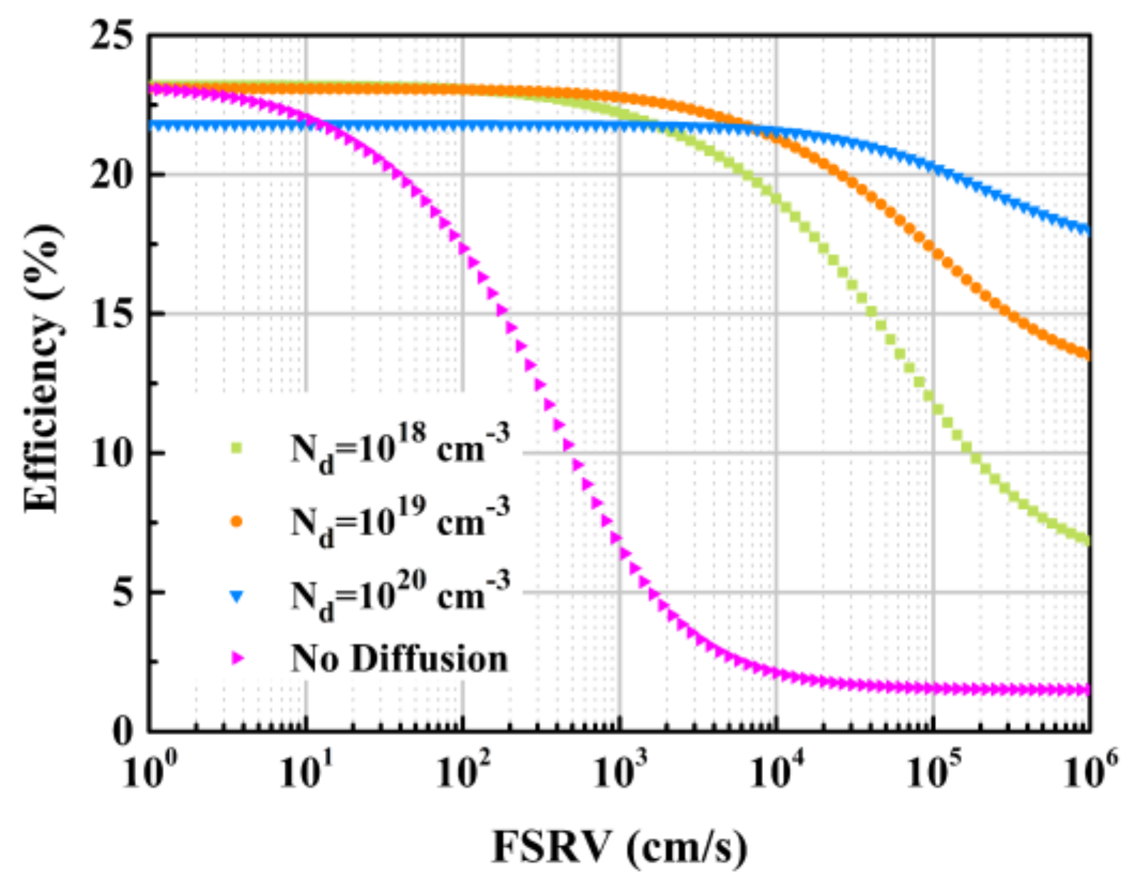
To understand the physical mechanisms driving the effects of the FSF concentration, PC1D software was used to simulate a simplified solar cell model according to the structure of the fabricated IBC cell. As shown in Figure 3, the cell efficiency was considerably dependent on the carrier FSRV in the studied IBC solar cell. The efficiencies of the solar cells with different front surface doping concentrations were almost identical when the FSRV < 3 cm/s.
A dramatic degradation occurred in the efficiency of the undoped solar cell as the FSRV reached 3 cm/s; the efficiency fell to 2.7% at an FSRV of approximately 5000 cm/s. Within the same FSRV range, the IBC solar cells with a doped front surface layer exhibited a much higher efficiency. In contrast, the performance of the cells with a doped front surface layer was far less sensitive to increasing the FSRV even if the FSRV was up to 104 cm/s. This was because in the absence of the n+ front surface doping layers, the front surface recombination was only affected by the variation in the FSRV. More specifically, a higher FSRV resulted in the higher recombination of the minority carriers and lower performance. By introducing the FSF structure, minority carriers were repelled away from the front surface, thus contributing to a decreased front surface recombination. In a practical industrial setting, a front surface doping layer is of great importance to obtain a low front surface recombination because realizing the FSRV < 3 cm/s via the industrial deposition of SiO2/SiNX coating is a significant challenge.
In Figure 3, the efficiency of cells with a front surface layer doping at Nd = 1018 cm−3 and Nd = 1019 cm−3 remained at ≈23% as the FSRV varied from 1 to 200 cm/s; it was approximately 1.3% lower for the front layer doping at Nd = 1020 cm−3 and a same range of FSRV. This can be explained by a tradeoff between the Auger recombination because of the doping in the front surface layer and the positive effect of the high-low junction formed by the n+ front surface doping layer and the n base. Both physical phenomena are strongly influenced by the doping concentration in the front layer.
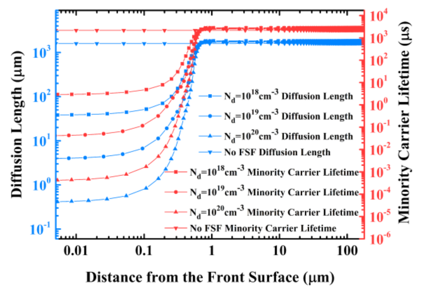
The relationship between the Auger recombination and the front surface doping concentration was simulated considering carrier transmission mechanisms. Figure 4 shows the diffusion length and minority carrier lifetime as a function of the distance from the front surface of the IBC solar cell for different FSF doping concentrations. The diffusion length of the FSF region at Nd = 1018 cm−3, 1019 cm−3 and 1020 cm−3 was ca. 38 μm, 4 μm and 0.4 μm, respectively; the minority carrier lifetime of the FSF region at the same concentration was ca. 3 μs, 0.04 μs and 4.2 × 10⁻⁴ μs, respectively. The Auger lifetime and doping concentration are inversely proportional; decreasing the FSF doping concentration weakens the Auger recombination, thus increasing the Auger lifetime in the doped front surface layer. On the other hand, the positive effect caused by the increased FSF doping concentration is not significant because the surface recombination of the minority carriers is inactive for FSRV < 200 cm/s. Therefore, under low FSRV conditions, decreased front surface doping concentration in the cell resulted in improved solar cell performance.
However, samples with an FSF doping concentration of 1020 cm−3 achieved the highest efficiency for FSRVs greater than 104 cm/s. At high FSRV, it is crucially important to suppress the front surface recombination by reducing the concentration of minority carriers near the front surface because surface recombination is proportional to the density of surface minority carriers. Note that the increase in FSF doping concentration enhances the electric field of the FSF, decreasing the minority carrier concentration near the front surface. Although the increased FSF doping concentration leads to a high Auger recombination, the enhanced suppression of surface recombination dominates at high FSRV conditions. Therefore, under high FSRV conditions, a drop in the doping concentration of the front surface layer is detrimental to the output performance.
As shown in Figure 3, under moderate FSRV conditions, the maximum efficiency was obtained with an FSF doping concentration of 1019 cm−3. This optimal front surface doping concentration reached the best counter-balance between the surface recombination and Auger recombination.
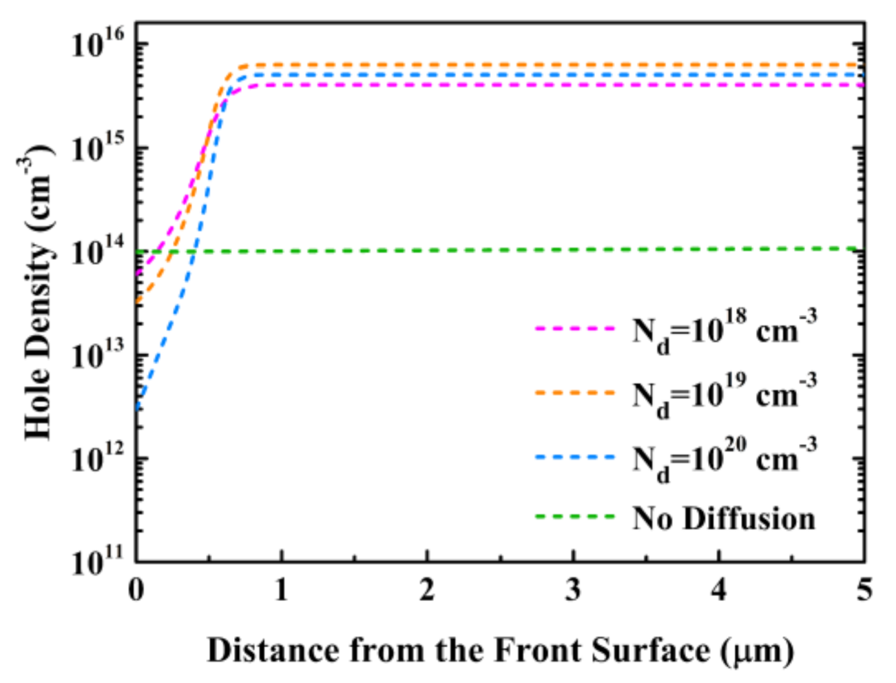
To further investigate and verify the presented analysis considering the carrier transmission mechanisms, the minority carrier (hole) density was examined with the distance from the front cell surface for an FSRV of 2000 cm s−1 [26] as shown in Figure 5.
As shown in Figure 5, the base hole density in a cell where no front surface doping layer was present was almost two orders of magnitude lower than that in IBC cells with a front surface doping layer. Note that surface recombination leads to a decline in the hole density at the front surface. Due to the hole density gradient, the holes (minority carriers) transfer from the base to the front surface. For the conditions used in this work, a lower hole density in the base suggested a higher combination at the front surface. When no front surface doping layer was present, a high hole density could be found at the front surface of the IBC solar cell because minority carriers were not repelled away, thus leading to a much higher front surface recombination than that in IBC cells with a doped front surface layer. Therefore, the hole density minimized in the n-type base.
The hole density in the base first increased and then decreased as the front surface doping concentration increased. Note that the minority carrier density in the base maximized at a front surface doping density of 1019 cm−3. The increased Auger recombination caused by the high FSF doping density and the enhanced positive electric field effect obtained from the raised doping concentration of the FSF layer reached a balance. When the FSF doping concentration was 1020 cm−3, the increase in Auger recombination dominated, thus leading to a lower hole density in the base when compared with that of the 1019 cm−3 doping density. This result and analysis verified the interpretation of the simulated IBC solar cell efficiency vs. FSRV (Figure 3) in terms of carrier transmission.
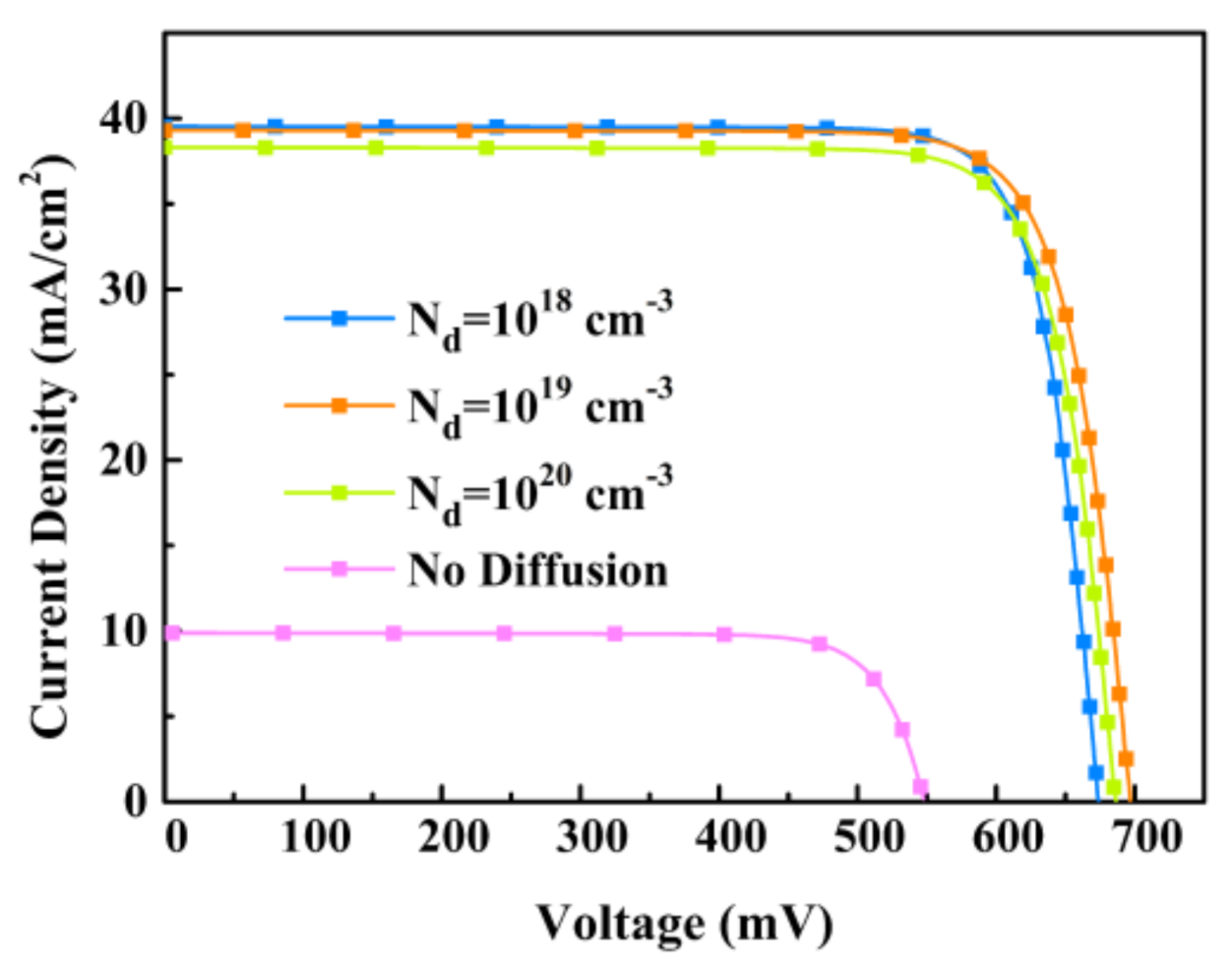
Figure 6 shows the simulated J-V curves of IBC solar cells under light for different FSF doping concentrations. The Jsc changed slightly as the FSF doping density varied from 1018 cm−3 to 1019 cm−3; the total change (reduction) in Jsc among the samples with a doped front surface layer Jsc was reduced by 1.25 mA/cm2 at an FSF doping concentration of 1020 cm−3 and Jsc was minimized in cells having no front surface doping layer. It is noteworthy that Jsc was determined by the collection probability [27], which can be derived with the following Equation (8) [28]:
J sc = q 0 w G x CP x dx  
In Equation (8), q denotes the electronic charge, w is the thickness of the solar cell, G(x) is the generation rate at position x and CP(x) represents the charge-collection probability. An increase in the front surface recombination leads to a decrease in the minority carrier lifetime, which results in a reduction of charge-collection probability. According to Equation (8), the degradation of the collection probability results in a much lower Jsc at the FSF doping concentration of 1020 cm−3 than that of the FSF doping level of 1019 cm−3 (Figure 6). Jsc is also influenced by the parasitic absorption because of FSF doping that reduces the carrier generation rate near the front surface of the IBC solar cell. When the FSF doping concentration increased, the incident light parasitic absorption became large at the front surface. Therefore, although the front surface recombination at the FSF doping concentration of 1018 cm−3 was greater than that at 1019 cm−3, the corresponding Jsc value was slightly higher than that at 1019 cm−3 (Figure 6). The presented analyses clarify the behavior of Jsc for all studied doping concentrations at the front surface in terms of carrier transmission mechanisms and charge-collection probability.

3.2. Experimental Results and Discussion

To validate the reliability of the simulation and its results, IBC cells with different doping concentrations in the front surface layer were fabricated and characterized. IBC solar cells without a doped front surface layer were also fabricated for reference.
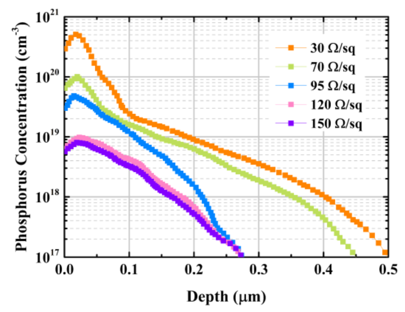
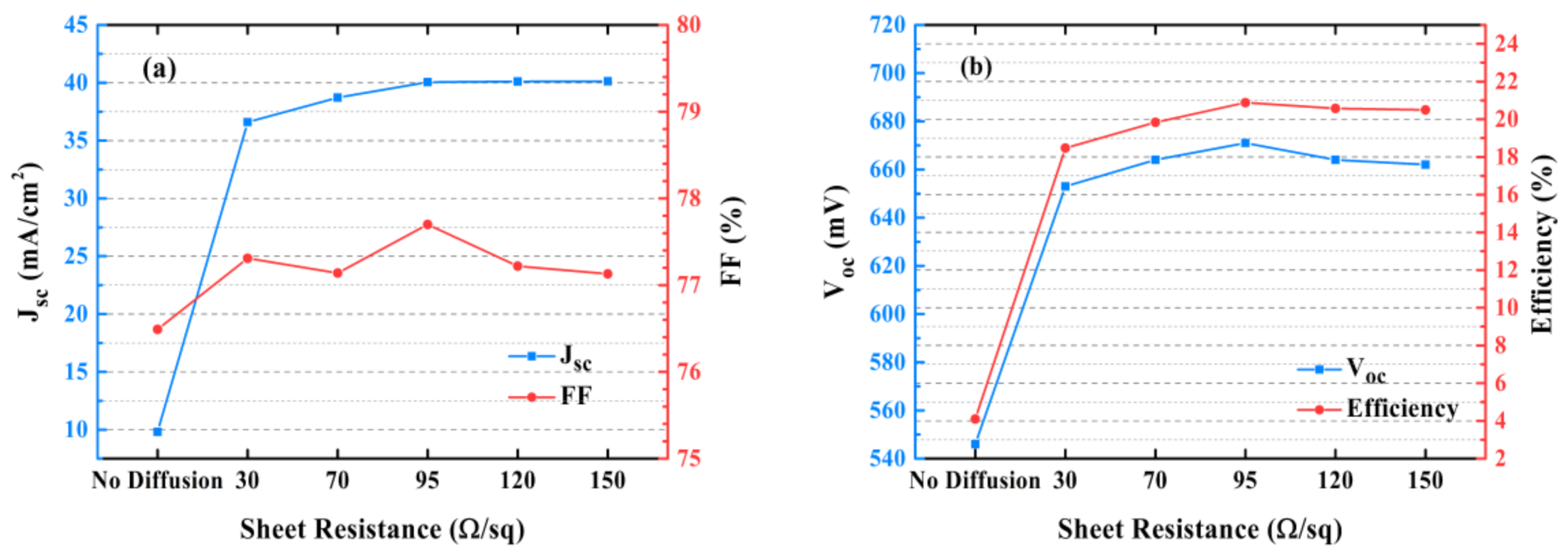
The phosphorus diffusion profile for the n+ front surface doping layers and the corresponding sheet resistance are shown in Figure 7. Note that the sheet resistance was inversely proportional to the phosphorus doping concentration of the front surface layer. The junction depth was 0.67 μm with the peak doping concentration of 4.8 × 1019 cm−3, which corresponded to a sheet resistance of 95 Ω/square. Figure 8 shows the measured electrical characteristics of the fabricated IBC cells that exhibited a range of doped front surface layer sheet resistances. Jsc increased from 36.59 to 40.13 mA/cm2 as the front surface layer doping concentration decreased, as shown in Figure 8a. The trend of Jsc with different FSF doping concentrations was similar with that of the simulated results. The performance of IBC cells without a front surface doping layer was poorer than that of cells with a front surface doping layer, thus demonstrating the importance and necessity to introduce an n+ FSF structure especially for industrial processes that are not capable of achieving ultralow FSRV.
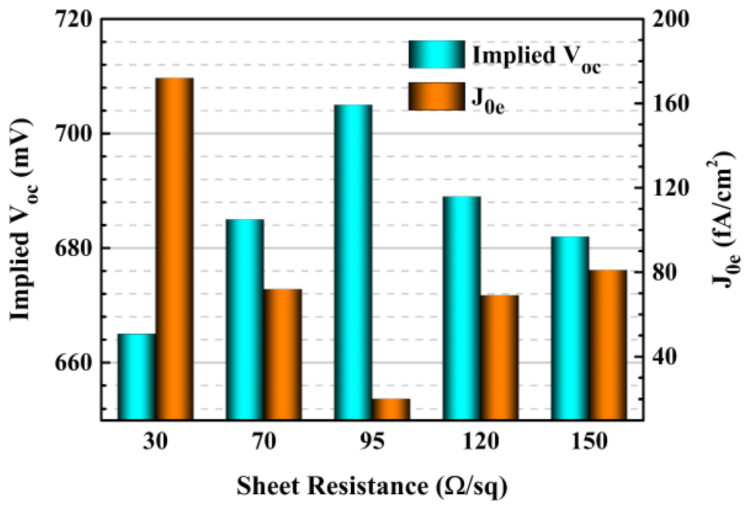
To understand the manner in which Jsc is related to the carrier transmission mechanism and charge-collection probability in the studied IBC solar cells, the variation in J0e and implied Voc with respect to the sheet resistance of the front surface doping layer was investigated. As shown in Figure 9, J0e decreased because of the reduced front surface recombination as the sheet resistance increased from 30 to 95 Ω/square whereas it increased when the sheet resistance exceeded 95 Ω/square caused by the increased recombination, which was attributed to the weakened electric field effect of the FSF. In contrast, the implied Voc exhibited an opposite trend than J0e for the same sheet resistance of the front surface doping layer. When the sheet resistance became 95 Ω/square corresponding to an FSF doping concentration of 4.8 × 1019 cm−3, J0e was optimal and the implied Voc was maximized at 705 mV. The essential parameters, J0e and implied Voc, which represented the passivation quality, were determined based on the minority carrier lifetime. An increase in J0e was associated with a reduction in the minority carrier lifetime, which reduced the collection probability. As Jsc was proportional to the collection probability shown in Equation (8), an increase in J0e decreased Jsc. Furthermore, although J0e increased when the front surface sheet resistance exceeded 95 Ω/square, Jsc was slightly greater than that at the sheet resistance of 95 Ω/square because of the reduced incident light parasitic absorption that could be attributed to the decreased FSF doping.
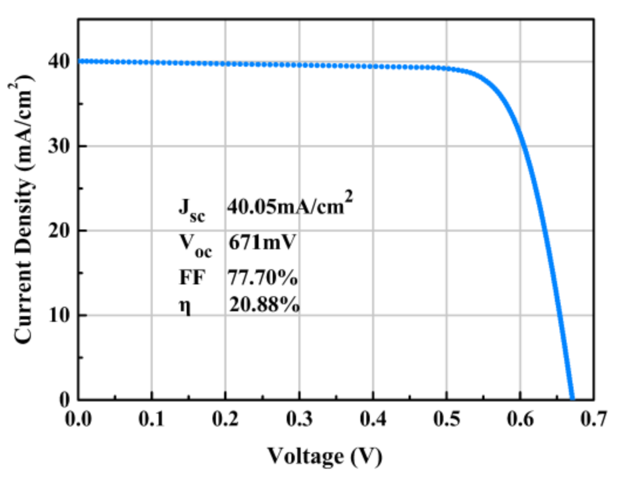
The J-V curve of the best IBC solar cell under light is shown in Figure 10; the sheet resistance of the front surface layer was 95 Ω/square. The maximum efficiency of the industrially feasible IBC solar cell reached 20.88%, with corresponding Voc = 671 mV, Jsc = 40.05 mA/cm2 and an FF of 77.70%. The experimentally optimized FSF doping concentration (i.e., corresponding to the sheet resistance of 95 Ω/square) was on the same order of magnitude with the simulated optimal FSF doping concentration. Furthermore, the trend of the measured Jsc agreed well with that of the simulated data. The experimental data demonstrated the validity and reliability of the simulation results and analyses.

4. Conclusions

The effects of different front surface doping levels in industrially feasible IBC solar cells were investigated systematically by simulation and experiment. Under different FSRVs, the optimum front surface doping concentration was achieved by balancing the increased Auger recombination and the enhanced positive electric field effect of the FSF. The minority carrier density in the base was highest in the best efficiency cell and it increased as the recombination in the doped front surface decreased. In industrial conditions, the introduction of a doped front surface layer was necessary because it could not realize ultralow FSRV by large-area SiO2/SiNx deposition. The simulated Jsc increased with a decrease in the front surface doping concentration because of the high charge-collection probability and the weakened parasitic absorption, which agrees with the experimental results and analysis of J0e and implied Voc. In addition, industrially feasible photolithography-free IBC solar cells featuring different front surface layer doping concentrations were fabricated in a commercial pilot line using laser ablation and screen printing. Instead of the conventional POCl3 diffusion, phosphorus paste screen printing and a thermal drive-in were applied to obtain the n+ BSF to avoid reducing the minority carrier lifetime caused by long thermal treatment. The highest efficiency of 20.88% was achieved with the optimum front surface doping concentration of 4.8 × 1019 cm−3. The trends of experimental results agree with those of the simulation data, thus indicating the validity and reliability of the simulation results and corresponding analysis.

Author Contributions

Conceptualization, methodology, software, validation, formal analysis, experiment, investigation, data curation, writing, visualization, X.L.; supervision, A.L. All authors have read and agreed to the published version of the manuscript.

Funding

This research received no external funding.

Conflicts of Interest

The authors declare no conflict of interest.

References

  1. Müller, R.; Reichel, C.; Yang, X.; Richter, A.; Benick, J.; Hermle, M. Impact of the homogeneous junction breakdown in IBC solar cells on the passivation quality of Al2O3 and SiO2: Degradation and regeneration behavior. Energy Procedia 2017, 124, 365–370. [Google Scholar] [CrossRef] [Green Version]
  2. Tachibana, T.; Mochizuki, T.; Shirasawa, K.; Takato, H. An investigation of internal quantum efficiency of bifacial interdigitated back contact (IBC) crystalline silicon solar cell. IEEE J. Photovolt. 2019, 9, 1526–1531. [Google Scholar] [CrossRef]
  3. Green, M.A.; Dunlop, E.D.; Hohl-Ebinger, J.; Yoshita, M.; Kopidakis, N.; Ho-Baillie, A.W.Y. Solar cell efficiency tables (Version 55). Prog. Photovolt. Res. Appl. 2020, 28, 3–15. [Google Scholar] [CrossRef]
  4. Guillevin, N.; Cesar, I.; Burgers, A.R.; Venema, P.; Wang, Z.; Zhai, J.Y.; Liu, D. Pilot line results of n-type IBC cell process in mass production environment. In Proceedings of the European Photovoltaic Solar Energy Conference and Exhibition, Amsterdam, The Netherlands, 25–29 September 2017; pp. 205–211. [Google Scholar]
  5. Liu, J.; Yao, Y.; Xiao, S.; Gu, X. Review of status developments of high-efficiency crystalline silicon solar cells. J. Phys. D Appl. Phys. 2018, 51, 123001. [Google Scholar] [CrossRef]
  6. Ingenito, A.; Isabella, O.; Zeman, M. Simplified process for high efficiency, self-aligned IBC c-Si solar cells combining ion implantation and epitaxial growth: Design and fabrication. Sol. Energy Mater. Sol. Cells 2016, 157, 354–365. [Google Scholar] [CrossRef]
  7. Franklin, E.; Fong, K.; Mclntosh, K.; Fell, A.; Blakers, A.; Kho, T.; Walter, D.; Wang, D.; Zin, N.; Stocks, M.; et al. Design, fabrication and characterisation of a 24.4% efficient interdigitated back contact solar cell. Prog. Photovolt. Res. Appl. 2016, 24, 411–427. [Google Scholar] [CrossRef]
  8. Li, Q.; Tao, K.; Sun, Y.; Jia, R.; Wang, S.; Jin, Z.; Liu, X. Two dimensional simulation studies on amorphous silicon stack as front surface field for interdigitated back contact solar cells. Vacuum 2016, 125, 56–64. [Google Scholar] [CrossRef]
  9. Chen, Y.; Yang, Y.; Marmon, J.K.; Zhang, X.; Feng, Z.; Verlinden, P.J.; Shen, H. Independent Al2O3/SiNx:H and SiO2/SiNx:H passivation of p+ and n+ silicon surfaces for high-performance interdigitated back contact solar cells. IEEE J. Photovolt. 2017, 7, 51–57. [Google Scholar] [CrossRef]
  10. Hollemann, C.; Haase, F.; Schäfer, S.; Krügener, J.; Brendel, R.; Peibst, R. 26.1%—Efficient POLO—IBC cells: Quantification of electrical and optical loss mechanisms. Prog. Photovolt. Res. Appl. 2019, 27, 950–958. [Google Scholar] [CrossRef]
  11. Yoshikawa, K.; Kawasaki, H.; Yoshida, W.; Irie, T.; Konishi, K.; Nakano, K.; Uto, T.; Adachi, D.; Kanematsu, M.; Uzu, H.; et al. Silicon heterojunction solar cell with interdigitated back contacts for a photoconversion efficiency over 26%. Nat. Energy 2017, 2, 17032. [Google Scholar] [CrossRef]
  12. Procel, P.; Yang, G.; Isabella, O.; Zeman, M. Theoretical evaluation of contact stack for high efficiency IBC-SHJ solar cells. Sol. Energy Mater. Sol. Cells 2018, 186, 66–77. [Google Scholar] [CrossRef]
  13. Lin, H.; Ding, D.; Wang, Z.; Zhang, L.; Wu, F.; Yu, J.; Gao, P.; Ye, J.; Shen, W. Realization of interdigitated back contact silicon solar cells by using dopant-free heterocontacts for both polarities. Nano Energy 2018, 50, 777–784. [Google Scholar] [CrossRef]
  14. Hashmi, G.; Akand, A.R.; Hoq, M.; Rahman, H. Study of the enhancement of the efficiency of the monocrystalline silicon solar cell by optimizing effective parameters using PC1D simulation. Silicon 2018, 10, 1653–1660. [Google Scholar] [CrossRef]
  15. Clugston, D.A.; Basore, P.A. PC1D version 5: 32-bit solar cell modeling on personal computers. In Proceedings of the 26th IEEE Photovoltaic Specialists Conference, Anaheim, CA, USA, 29 September–3 October 1997; pp. 207–210. [Google Scholar]
  16. Cho, E.; Ok, Y.; Dahal, L.D.; Das, A.; Upadhyaya, V.; Rohatgi, A. Comparison of POCl3 diffusion and phosphorus ion-implantation induced gettering in crystalline Si solar cells. Sol. Energy Mater. Sol. Cells 2016, 157, 245–249. [Google Scholar] [CrossRef] [Green Version]
  17. Uprety, P.; Subedi, I.; Junda, M.M.; Collins, R.W.; Podraza, N.J. Photogenerated carrier transport properties in silicon photovoltaics. Sci. Rep. 2019, 9, 19015. [Google Scholar] [CrossRef] [PubMed] [Green Version]
  18. Onno, A.; Chen, C.; Koswatta, P.; Boccard, M.; Holman, Z.C. Passivation, conductivity, and selectivity in solar cell contacts: Concepts and simulations based on a unified partial-resistances framework. J. Appl. Phys. 2019, 126, 183103. [Google Scholar] [CrossRef]
  19. Haug, H.; Olaisen, B.R.; Nordseth, Ø.; Marstein, E.S. A graphical user interface for multivariable analysis of silicon solar cells using scripted PC1D simulations. Energy Procedia 2013, 38, 72–79. [Google Scholar] [CrossRef] [Green Version]
  20. Singha, B.; Solanki, C.S. Optimization of boron spin on dopant (BSoD) diffusion for emitter formation in n-type c-Si solar cells. Mater. Today Proc. 2018, 5, 23466–23471. [Google Scholar] [CrossRef]
  21. Geerligs, L.J.; Macdonald, D. Base doping and recombination activity of impurities in crystalline silicon solar cells. Prog. Photovolt. Res. Appl. 2004, 12, 309–316. [Google Scholar] [CrossRef]
  22. Haug, H.; Greulich, J. PC1Dmod 6.2—Improved simulation of c-Si devices with updates on device physics and user interface. Energy Procedia 2016, 92, 60–68. [Google Scholar] [CrossRef]
  23. Basore, P.A.; Clugston, D.A. PC1D version 4 for windows: From analysis to design. In Proceedings of the 25th IEEE Photovoltaic Specialists Conference, Washington, DC, USA, 13–17 May 1996; pp. 377–381. [Google Scholar]
  24. Cai, X.; Zhou, X.; Liu, Z.; Jiang, F.; Yu, Q. An in-depth analysis of the silicon solar cell key parameters’ optimal magnitudes using PC1D simulations. Optik 2018, 164, 105–113. [Google Scholar] [CrossRef]
  25. Altermatt, P.P.; Schenk, A.; Geelhaar, F.; Heiser, G. Reassessment of the intrinsic carrier density in crystalline silicon in view of band-gap narrowing. J. Appl. Phys. 2003, 93, 1598–1604. [Google Scholar] [CrossRef]
  26. Altermatt, P.P.; Schumacher, J.O.; Cuevas, A.; Kerr, M.J.; Glunz, S.W.; King, R.R.; Heiser, G.; Schenk, A. Numerical modeling of highly doped Si:P emitters based on Fermi-Dirac statistics and self-consistent material parameters. J. Appl. Phys. 2002, 92, 3187–3197. [Google Scholar] [CrossRef] [Green Version]
  27. Zandi, S.; Saxena, P.; Razaghi, M.; Gorji, N.E. Simulation of CZTSSe thin-film solar cells in COMSOL: Three-dimensional optical, electrical, and thermal models. IEEE J. Photovolt. 2020, 10, 1503–1507. [Google Scholar] [CrossRef]
  28. Hermle, M.; Granek, F.; Schultz, O.; Glunz, S.W. Analyzing the effects of front-surface fields on back-junction silicon solar cells using the charge-collection probability and the reciprocity theorem. J. Appl. Phys. 2008, 103, 54507. [Google Scholar] [CrossRef]
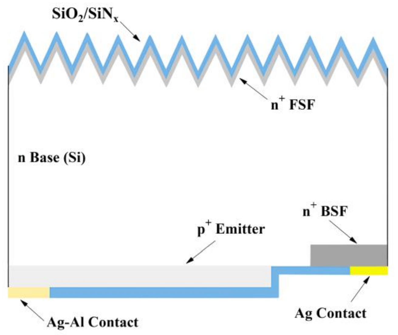
Figure 1. Schematic of the cross section of the studied industrially viable interdigitated back contact (IBC) solar cell.
Energies 13 05303 g001
Figure 2. The process flow for fabricating the presented low-cost, industrially feasible IBC solar cell with laser ablation and screen printing. BS, FS and DS represent back side, front side and double sides respectively. FSF and BSF denote front surface field and back surface field respectively.
Energies 13 05303 g002
Figure 3. Efficiencies of the simulated IBC solar cells as a function of the front surface recombination velocity (FSRV). Nd indicates the front surface layer doping concentration. The efficiencies of the undoped front surface control samples are shown in magenta. Each doping junction depth was fixed at 0.67 μm and the lines are guides for the eye.
Energies 13 05303 g003
Figure 4. Diffusion length and minority carrier lifetime versus distance from the front surface of the IBC solar cell model for different front surface field (FSF) doping concentrations.
Energies 13 05303 g004
Figure 5. Variation in the hole density as a function of the distance from the front surface of the IBC solar cell model for different front surface layer doping concentrations. The FSRV is 2000 cm/s in all curves.
Energies 13 05303 g005
Figure 6. Simulated current-density voltage (J-V) curves of solar cells under light for different FSF doping concentrations.
Energies 13 05303 g006
Figure 7. Electrochemical capacitance-voltage (ECV) profiles of front side phosphorus diffusion layers in the fabricated IBC solar cells; the sheet resistance was determined by four-point probe measurements.
Energies 13 05303 g007
Figure 8. IBC solar cell performance parameters, (a) Jsc and FF and (b) Voc and efficiency, as extracted from the J-V characteristics of the best fabricated IBC cells with different front surface layer doping conditions (i.e., different front surface layer sheet resistances) measured under AM 1.5G, 0.1 W/cm2 and 25 °C. No diffusion condition shows a control device made with no doped front surface layer. The active cell area was 2 × 2 cm2 in all the cells.
Energies 13 05303 g008
Figure 9. J0e and implied Voc as a function of different front surface doping layer sheet resistances (i.e., different FSF doping concentrations) of the fabricated IBC solar cell.
Energies 13 05303 g009
Figure 10. The J-V curve of the best IBC solar cell measured under AM 1.5G, 0.1 W/cm2 and 25 °C; the sample sheet resistance was 95 Ω/square at the front surface doped layer. The active cell area was 2 × 2 cm2.
Energies 13 05303 g010
Table 1. Parameters for this simulation work.
ParametersValues 1
Device area4 cm2
Front surface texture angle45°
Front surface texture depth3 μm
External front reflectance5%
Thickness180 μm
MaterialSilicon (Si)
Dielectric constant11.9
Band gap1.124 eV
Intrinsic carrier density [25]9.65 × 109 cm−3
Base dopant density1.15 × 1015 cm−3
n+ front layer dopant densityVary
n+ front layer thickness0.67 μm
Bulk recombination2 ms
Front surface recombinationVary
Back surface recombination100 cm s−1
Temperature25°
Constant intensity0.1 W cm−2
SpectrumAM 1.5G
1 Except for the n+ front layer dopant density and front surface recombination, these variables are consistent with those of the fabricated IBC solar cell.