Enabling a Battery-Less Sensor Node Using Dedicated Radio Frequency Energy Harvesting for Complete Off-Grid Applications


Abstract
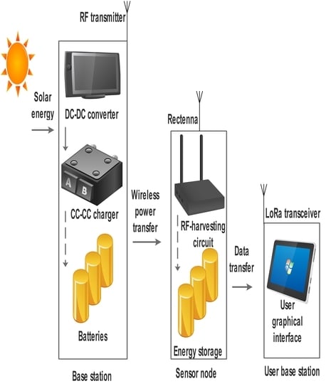
1. Introduction
- (1)
- We generate high voltage output from a low received RF power by designing an antenna with large gain and low return loss at 920 MHz.
- (2)
- We design and implement specific aspects of the proposed system including the DC-DC converter, CV-CV charging algorithm, microcontroller unit, microcontroller firmware and the sensor node energy storage circuitry.
- (3)
- We design and implement a proportional integral derivative (PID) to control the DC-DC converter to ensure a stable output current and voltage of the step-down DC-DC converter.
- (4)
- We develop a constant current-constant voltage (CC-CV battery) charging algorithm to effectively charge lithium-ion batteries to prevent permanent damage due to overvoltage or overcurrent conditions.
- (5)
- We develop an energy harvesting system that provides of power for a duration of once every min.
2. Related Works
3. Theory
4. Design Alternatives and Design Implementation
4.1. Power Base Station (FU1)
4.2. Step-Down DC-DC Converter Design (FU1.2)
4.3. Microcontroller Input Design
4.4. Microcontroller Firmware Design
4.5. PID Controller Design
4.6. Antenna (FU2.2)
4.7. Yagi Antenna Design
4.8. Energy Harvesting Circuit (FU2.2)
4.9. Energy Harvesting Circuit Design (FU2.2)
4.9.1. Fully Cross-Coupled RF-DC Converter
4.9.2. Step-Up DC-DC Converter
4.10. Design of the Multitech LoRa Communication
4.11. Sensor Node
5. Results and Discussion
5.1. Full System Test
5.2. Yagi Antenna Gain Test
5.3. Yagi Antenna Return Loss Test
5.4. CC-CV Charging of Li-Ion Battery Test
6. Summary of Results Achieved
7. Conclusions
Author Contributions
Funding
Conflicts of Interest
References
- Centenaro, M.; Vangelista, L.; Zanella, A.; Zorzi, M. Long-range communications in unlicensed bands: The rising stars in the IoT and smart city scenarios. IEEE Wirel. Commun. 2016, 23, 60–67. [Google Scholar] [CrossRef]
- Oyewobi, S.; Onwuka, E. Conservation of Mobile Terminals’ Battery Life Using Dynamic Power Control Algorithm. J. Wirel. Network. Commun. 2012, 2, 15–20. [Google Scholar]
- Shafique, K.; Khawaja, B.A.; Khurram, M.D.; Sibtain, S.M.; Siddiqui, Y.; Mustaqim, M.; Chattha, H.T.; Yang, X. Energy Harvesting Using a Low-Cost Rectenna for Internet of Things (IoT) Applications. IEEE Access 2018, 6, 30932–30941. [Google Scholar] [CrossRef]
- Oyewobi, S.; Onwuka, E.; Onumanyi, A. Mobile terminals energy: A survey of battery technologies and energy management techniques. Int. J. Eng. Technol. 2013, 3, 282–286. [Google Scholar]
- Minami, M.; Morito, T.; Morikawa, H.; Aoyama, T. Solar biscuit: A battery-less wireless sensor network system for environmental monitoring applications. In Proceedings of the 2nd International Workshop on Networked Sensing Systems, San Diego, CA, USA, 1 June 2005; p. 2007. [Google Scholar]
- Bader, S.; Oelmann, B. Enabling battery-less wireless sensor operation using solar energy harvesting at locations with limited solar radiation. In Proceedings of the 2010 Fourth International Conference on Sensor Technologies and Applications, Venice, Italy, 18–25 July 2010; pp. 602–608. [Google Scholar]
- Sikder, A.K.; Acar, A.; Aksu, H.; Uluagac, A.S.; Akkaya, K.; Conti, M. IoT-enabled smart lighting systems for smart cities. In Proceedings of the 2018 IEEE 8th Annual Computing and Communication Workshop and Conference (CCWC), Las Vegas, NV, USA, 8–10 January 2018; pp. 639–645. [Google Scholar]
- Saffari, A.; Hessar, M.; Naderiparizi, S.; Smith, J.R. Battery-free wireless video streaming camera system. In Proceedings of the 2019 IEEE International Conference on RFID (RFID), Phoenix, AZ, USA, 2–4 April 2019; pp. 1–8. [Google Scholar]
- Naderiparizi, S.; Hessar, M.; Talla, V.; Gollakota, S.; Smith, J.R. Towards battery-free {HD} video streaming. In Proceedings of the 15th {USENIX} Symposium on Networked Systems Design and Implementation ({NSDI} 18), Renton, WA, USA, 9–11 April 2018; pp. 233–247. [Google Scholar]
- Talla, V.; Kellogg, B.; Gollakota, S.; Smith, J.R. Battery-free cellphone. Proc. ACM Interact. Mobile Wearable Ubiquitous Technol. 2017, 1, 1–20. [Google Scholar] [CrossRef]
- Tresanchez, M.; Pujol, A.; Pallejà, T.; Martínez, D.; Clotet, E.; Palacín, J. An inexpensive wireless smart camera system for IoT applications based on an ARM Cortex-M7 microcontroller. J. Ubiquitous Syst. Pervasive Netw. 2019, 11, 01–08. [Google Scholar] [CrossRef]
- la Rosa, R.; Livreri, P.; Trigona, C.; di Donato, L.; Sorbello, G. Strategies and Techniques for Powering Wireless Sensor Nodes through Energy Harvesting and Wireless Power Transfer. Sensors 2019, 19, 2660. [Google Scholar] [CrossRef]
- Joannopoulos, J.D.; Karalis, A.; Soljacic, M. Wireless Non-Radiative Energy Transfer. U.S. Pantent 9450421B2, 20 September 2016. [Google Scholar]
- Oruganti, S.K.; Malik, J.; Lee, J.; Paul, D.; Park, W.; Lee, B.; Seo, S.; Kim, H.S.; Bien, F.; Thundat, T. Experimental and Theoretical Realization of Zenneck Wave-based Non-Radiative, Non-Coupled Wireless Power Transmission. arXiv 2019, arXiv:1903.10294. [Google Scholar]
- Wang, J.; Leach, M.; Lim, E.G.; Wang, Z.; Huang, Y. Investigation of magnetic resonance coupling circuit topologies for wireless power transmission. Microw. Opt. Technol. Lett. 2019, 61, 1755–1763. [Google Scholar] [CrossRef]
- Huang, J.; Zhou, Y.; Ning, Z.; Gharavi, H. Wireless Power Transfer and Energy Harvesting: Current Status and Future Prospects. IEEE Wirel. Commun. 2019, 26, 163–169. [Google Scholar] [CrossRef] [PubMed]
- Osepchuk, J.M.; Petersen, R.C. Historical review of RF exposure standards and the International Committee on Electromagnetic Safety (ICES). Bioelectromagnetics 2003, 24, S7–S16. [Google Scholar] [CrossRef]
- Bhattacharya, A.; De, A.; Biswas, A.; Roy, B.; Bhattacharjee, A.K. Application of Particle Swarm Optimization in Design of a Low-Profile Fractal Patch Antenna. In Advances in Computer, Communication and Control; Springer: Berlin, Germany, 2019; pp. 207–214. [Google Scholar]
- Huang, F.-J.; Yo, T.-C.; Lee, C.-M.; Luo, C.-H. Design of circular polarization antenna with harmonic suppression for rectenna application. IEEE Antennas Wirel. Propag. Lett. 2012, 11, 592–595. [Google Scholar] [CrossRef]
- Clenet, M.; Litzenberger, J.; Lee, D.; Thirakoune, S.; Morin, G.A.; Antar, Y.M. Laminated waveguide as radiating element for array applications. IEEE Trans. Antennas Propag. 2006, 54, 1481–1487. [Google Scholar] [CrossRef]
- Gong, Z.; Wan, K.; Shen, G.; Wan, X.; Wu, R.; Liu, Z.; Lu, Y.; Yin, J. An Ultra-Wideband Capped Bow-Tie Multilayer-Stacked Yagi Antenna. Prog. Electromagn. Res. 2019, 85, 9–16. [Google Scholar] [CrossRef]
- Wahid, P.; Ali, M.; DeLoach, B., Jr. A reconfigurable Yagi antenna for wireless communications. Microw. Opt. Technol. Lett. 2003, 38, 140–141. [Google Scholar] [CrossRef]
- Wu, J.; Zhao, Z.; Nie, Z.; Liu, Q.-H. Bandwidth enhancement of a planar printed quasi-Yagi antenna with size reduction. IEEE Trans. Antennas Propag. 2013, 62, 463–467. [Google Scholar] [CrossRef]
- Galal, H.; Flatae, A.M.; Lagomarsino, S.; Schulte, G.; Wild, C.; Wörner, E.; Gelli, N.; Sciortino, S.; Schönherr, H.; Giuntini, L.; et al. Highly efficient light extraction and directional emission from diamond color centers using planar Yagi-Uda antennas. arXiv 2019, arXiv:1905.03363. [Google Scholar]
- Yao, L.; Mao, H.; Batarseh, I.E. A rectification topology for high-current isolated DC-DC converters. IEEE Trans. Power Electron. 2007, 22, 1522–1530. [Google Scholar] [CrossRef]
- Sudevalayam, S.; Kulkarni, P. Energy harvesting sensor nodes: Survey and implications. IEEE Commun. Surv. Tutor. 2011, 13, 443–461. [Google Scholar] [CrossRef]
- Assimonis, S.D.; Daskalakis, S.-N.; Bletsas, A. Sensitive and efficient RF harvesting supply for batteryless backscatter sensor networks. IEEE Trans. Microw. Theory Tech. 2016, 64, 1327–1338. [Google Scholar] [CrossRef]
- Assimonis, S.D.; Fusco, V.; Georgiadis, A.; Samaras, T. Efficient and sensitive electrically small rectenna for ultra-low power RF energy harvesting. Sci. Rep. 2018, 8, 1–13. [Google Scholar] [CrossRef] [PubMed]
- Khullar, V.; Tyagi, H.; Phelan, P.E.; Otanicar, T.P.; Singh, H.; Taylor, R.A. Solar energy harvesting using nanofluids-based concentrating solar collector. J. Nanotechnol Eng. Med. 2012, 3, 031003. [Google Scholar] [CrossRef]
- Pournoori, N.; Khan, M.W.A.; Ukkonen, L.; Björninen, T. RF Energy Harvesting System Integrating a Passive UHF RFID Tag as a Charge Storage Indicator. In Proceedings of the 2018 IEEE International Symposium on Antennas and Propagation & USNC/URSI National Radio Science Meeting, Boston, MA, USA, 8–13 July 2018; pp. 685–686. [Google Scholar]
- Ha, B.W.; Park, J.A.; Jin, H.J.; Cho, C.S. Energy transfer and harvesting for RF-Bio applications. In Proceedings of the 2015 IEEE MTT-S 2015 International Microwave Workshop Series on RF and Wireless Technologies for Biomedical and Healthcare Applications (IMWS-BIO), Taipei, Taiwan, 21–23 September 2015; pp. 54–55. [Google Scholar]
- Nalini, M.; Kumar, J.N.; Kumar, R.M.; Vignesh, M. Energy harvesting and management from ambient RF radiation. In Proceedings of the 2017 International Conference on Innovations in Green Energy and Healthcare Technologies (IGEHT), Coimbatore, India, 16–18 March 2017; pp. 1–3. [Google Scholar]
- Alkheir, A.A.; Mouftah, H.T. Exact statistical characterization of rf-energy harvesting over rice fading channel. In Proceedings of the 2018 IEEE Wireless Power Transfer Conference (WPTC), Montreal, QC, Canada, 3–7 June 2018; pp. 1–4. [Google Scholar]
- Lakshmi, P.S.; Jibukumar, M.; Neenu, V. Network lifetime enhancement of multi-hop wireless sensor network by RF energy harvesting. In Proceedings of the 2018 International Conference on Information Networking (ICOIN), Chiang Mai, Thailand, 10–12 January 2018; pp. 738–743. [Google Scholar]
- Xu, W.; Kim, J.Y.; Huang, W.; Kanhere, S.; Jha, S.; Hu, W. Measurement, Characterization and Modeling of LoRa Technology in Multi-floor Buildings. IEEE Internet Things J. 2019, 7, 298–310. [Google Scholar] [CrossRef]
- Chevalier, M.; Gomez-Schiavon, M.; Ng, A.H.; El-Samad, H. Design and analysis of a proportional-integral-derivative controller with biological molecules. Cell Syst. 2019, 9, 338–353.e10. [Google Scholar] [CrossRef] [PubMed]
- Liang, Y.; Xu, S.; Hong, K.; Wang, G.; Zeng, T. Neural network modeling and single-neuron proportional–integral–derivative control for hysteresis in piezoelectric actuators. Meas. Control 2019, 52, 1362–1370. [Google Scholar] [CrossRef]
- Eissa, M.A. Novel Fuzzy-Based Self-Adaptive Single Neuron PID Load Frequency Controller for Power System. Power Electron. Drives 2019, 4, 141–150. [Google Scholar] [CrossRef]
- Sun, Y.; Liu, Y.; Tang, N.; Xu, D.; Li, Y.; Yu, Y.; Zhang, K.; Gou, Q.; Du, Z. The design of wideband Quasi-Yagi elliptic dipole antenna with split-ring resonator (SRR) structures. In Proceedings of the 2018 International Workshop on Antenna Technology (iWAT), Nanjing, China, 5–7 March 2018; pp. 1–3. [Google Scholar]
- Viezbicke, P.P. Yagi Antenna Design; US Government Printing Office: Washington, DC, USA, 1976. [Google Scholar]
- Balanis, C.A. Antenna Theory: Analysis and Design; John wiley & Sons: Hoboken, NJ, USA, 2016. [Google Scholar]
- Zhou, W.; Tong, Z.; Dong, Z.Y.; Wang, Y. LoRa-Hybrid: A LoRaWAN Based Multihop Solution for Regional Microgrid. In Proceedings of the 2019 IEEE 4th International Conference on Computer and Communication Systems (ICCCS), Singapore, 23–25 February 2019; pp. 650–654. [Google Scholar]
- Kim, D.-H.; Lee, E.-K.; Kim, J. Experiencing LoRa Network Establishment on a Smart Energy Campus Testbed. Sustainability 2019, 11, 1917. [Google Scholar] [CrossRef]


| Deliverables | Designed and Implemented | Off-the-Shelf | Location of Each Deliverables |
|---|---|---|---|
| Solar panel | 🗸 | FU1.1 | |
| Battery | 🗸 | FU1.4 | |
| DC-DC converter | 🗸 | FU1.2 | |
| CC-CV charging circuit | 🗸 | FU1.3 | |
| RF transmitter | 🗸 | FU1.5 | |
| RF transmitter amplifier | 🗸 | FU1.6 | |
| RF transmitter antenna | 🗸 | FU1.7 | |
| Temperature sensor | 🗸 | FU2.4 | |
| LCD screen | 🗸 | FU3.2 | |
| LoRa transceiver | 🗸 | FU2.5/FU3.1 | |
| Microcontroller unit | 🗸 | FU1.2/FU1.3 | |
| Microcontroller firmware | 🗸 | FU1.2/FU1.3 | |
| Rectenna | 🗸 | FU2.1 | |
| RF harvesting circuit | 🗸 | FU2.2 | |
| Sensor node energy storage circuitry | 🗸 | FU2.3 |
| Feature | Required | PIC32MX220F032 |
|---|---|---|
| ADC inputs | 3 | 9 |
| ADC resolutions | 10 bits | 10 bits |
| PWM outputs | 1 | 16 |
| PWM resolutions | 10 bits | 10 bits with an instruction clock frequency of 40 MHz and a PWM frequency of 50 kHz |
| Instruction clock frequency | 1 MHz | Up to 40 MHz |
| PID controller | 0.313 | 2.2 |
| Element | Spacing from the Driven Element (mm) | Length (mm) | Diameter (mm) |
|---|---|---|---|
| Reflector | 64.5 | 169.55 | 6.35 |
| Driven | 0 | 184.1 | 6.00 |
| Director 1 | 26.2 | 150.3 | 6.35 |
| Director 2 | 86.6 | 149.4 | 6.35 |
| Director 3 | 157.6 | 146.1 | 6.35 |
| Director 4 | 239.4 | 145.7 | 6.35 |
| Director 5 | 333.6 | 144.4 | 6.35 |
| Director 6 | 434.2 | 139.8 | 6.35 |
| Director 7 | 538.7 | 141.4 | 6.35 |
| Director 8 | 647.9 | 140.8 | 6.35 |
| Director 9 | 760.2 | 140.0 | 6.35 |
| Director 10 | 879.5 | 137.6 | 6.35 |
| Temperature Sensor | Dallas 18B20 | Microchip MCP9700 |
|---|---|---|
| Operating Voltage | 3.0 to 5.0 V | 2.3 to 5.5 V |
| Accuracy | °C | °C |
| Standby Current | 900 | 6 |
| Active Current | 1 | 6 |
| Temperature Conversion Time | 750 | N/A |
| S/N | Intended Outcome | Actual Outcome |
|---|---|---|
| 1 | The power base station should be remote (does not have access to the grid) and derive its power via solar energy. | The power base station was able to derive its power from the solar panel. |
| 2 | The power outputted by the solar panel should be conditioned by a DC-DC converter as well as a CCCV (Continuous Current—Continuous Voltage) battery charger to charge the battery correctly. | The batteries were charged correctly through the implementation of a CC-CV charging algorithm controlling the DC-DC converter. |
| 3 | The power base station should provide RF energy to the sensor node. | The power base station provided RF energy to the sensor node. |
| 4 | The sensor node should be battery-less and wireless. | The sensor node was battery-less and wireless |
| 5 | Energy stored by the energy harvesting system should provide power to the sensor node’s temperature sensor, microcontroller, and LoRa transceiver. | Energy stored by the energy harvesting system provided power to the sensor node’s temperature sensor, microcontroller, and LoRa transceiver. |
| 6 | The sensor node should collect data (the sensed temperature) and communicate this data to the user base station using the LoRa LPWAN protocol. | The sensor node collected data and communicated the data to the user base station. |
| 7 | The system should measure temperature once every 60 min. | The system measured temperature once every 156 min. |
| 8 | The gain of the rectenna should be at least 1 dBi. | The gain of the antenna was 12.62 dBi |
| 9 | The voltage applied to the terminals of the battery while charging should not exceed the rated battery charging voltage. For Li-ion (Lithium-ion), this value is 4.2 V. | The voltage applied to the terminals of the battery did not exceed 4.21 V per battery. |
| 10 | The current delivered to the battery while charging should not exceed the rated battery charging current. For Li-ion batteries this value is half of the rated battery capacity given in mAh. | The current delivered to the battery while charging did not exceed 1.11 A. |
| 11 | The energy harvesting method should provide a minimum voltage of 1.8 V. | The energy harvesting circuit was able to provide 3.3 V. |
| 12 | The temperature should be measured once every 60 min. | The temperature was measured once every 156 min |
| 13 | The frequency of the RF transmitter should be 920 MHz ± 1.5 kHz. The transmitted RF should be CW (continuous wave) RF. | The frequency of the RF transmitter was 920 MHz ± 1.5 kHz and was a CW. |
| 14 | The step-down DC-DC converter, CC-CV charging control system hardware and software, sensor antenna, RF energy harvesting circuit, sensor node energy storage circuitry, sensor node microcontroller firmware should be designed and implemented. | The step-down DC-DC converter, CC-CV charging control system hardware and software, sensor antenna, RF energy harvesting circuit, sensor node energy storage circuitry, sensor node microcontroller firmware were all designed and implemented. |
Publisher’s Note: MDPI stays neutral with regard to jurisdictional claims in published maps and institutional affiliations. |
© 2020 by the authors. Licensee MDPI, Basel, Switzerland. This article is an open access article distributed under the terms and conditions of the Creative Commons Attribution (CC BY) license (http://creativecommons.org/licenses/by/4.0/).
Share and Cite
Miller, T.; Oyewobi, S.S.; Abu-Mahfouz, A.M.; Hancke, G.P. Enabling a Battery-Less Sensor Node Using Dedicated Radio Frequency Energy Harvesting for Complete Off-Grid Applications. Energies 2020, 13, 5402. https://doi.org/10.3390/en13205402
Miller T, Oyewobi SS, Abu-Mahfouz AM, Hancke GP. Enabling a Battery-Less Sensor Node Using Dedicated Radio Frequency Energy Harvesting for Complete Off-Grid Applications. Energies. 2020; 13(20):5402. https://doi.org/10.3390/en13205402
Chicago/Turabian StyleMiller, Timothy, Stephen S. Oyewobi, Adnan M. Abu-Mahfouz, and Gerhard P. Hancke. 2020. "Enabling a Battery-Less Sensor Node Using Dedicated Radio Frequency Energy Harvesting for Complete Off-Grid Applications" Energies 13, no. 20: 5402. https://doi.org/10.3390/en13205402
APA StyleMiller, T., Oyewobi, S. S., Abu-Mahfouz, A. M., & Hancke, G. P. (2020). Enabling a Battery-Less Sensor Node Using Dedicated Radio Frequency Energy Harvesting for Complete Off-Grid Applications. Energies, 13(20), 5402. https://doi.org/10.3390/en13205402