Hybrid DC Converter with Current Sharing and Low Freewheeling Current Loss

Abstract
:
1. Introduction
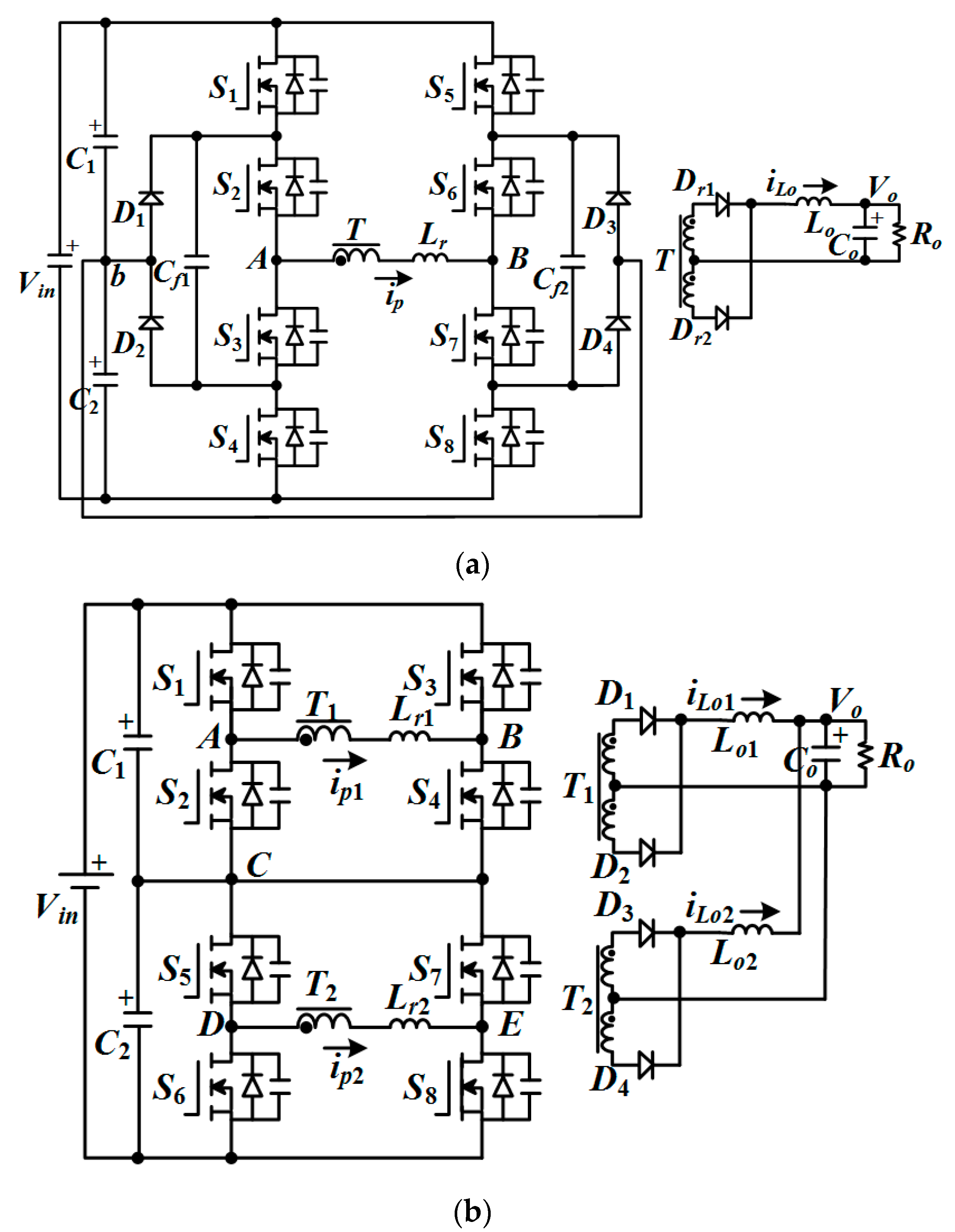
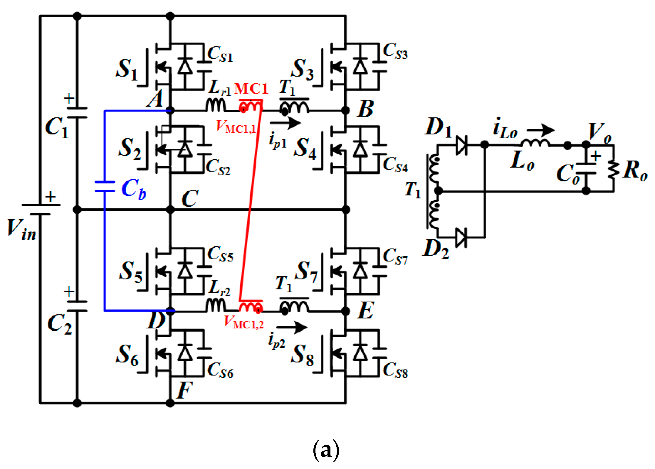
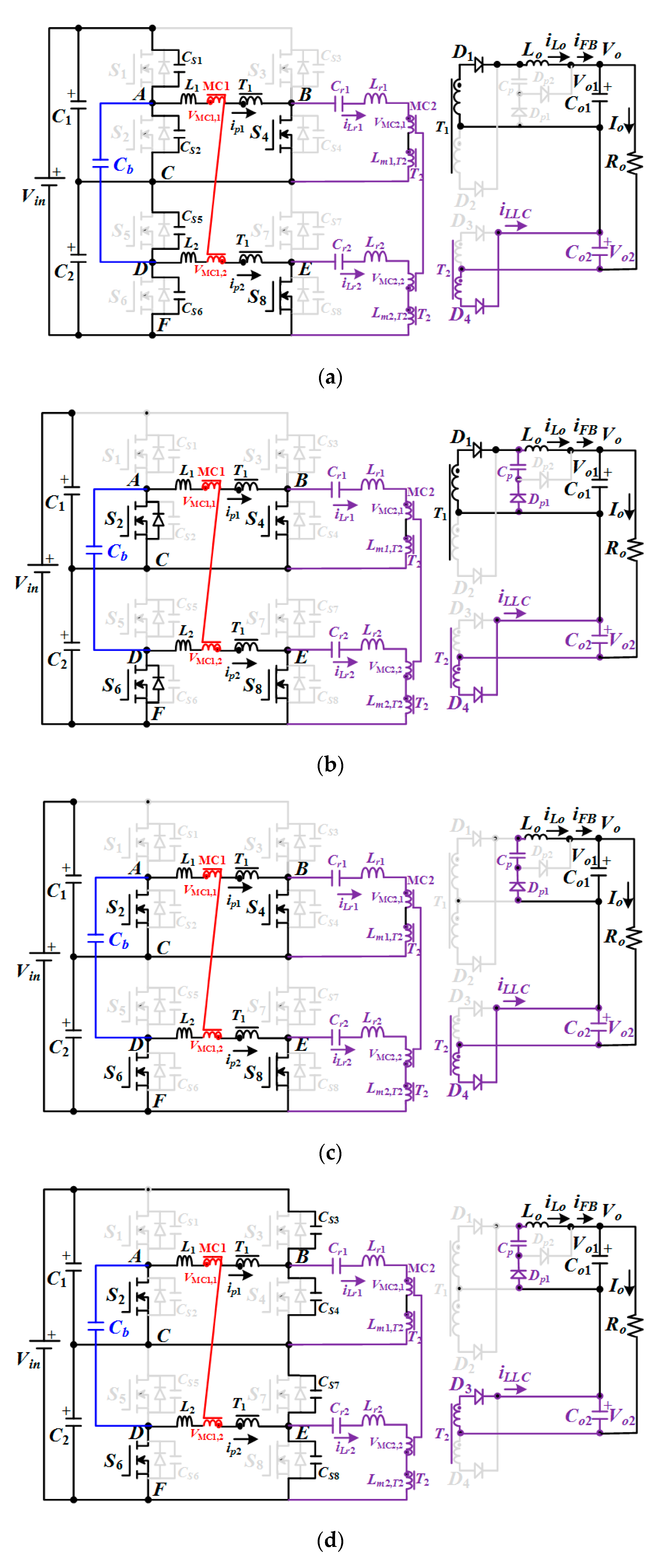
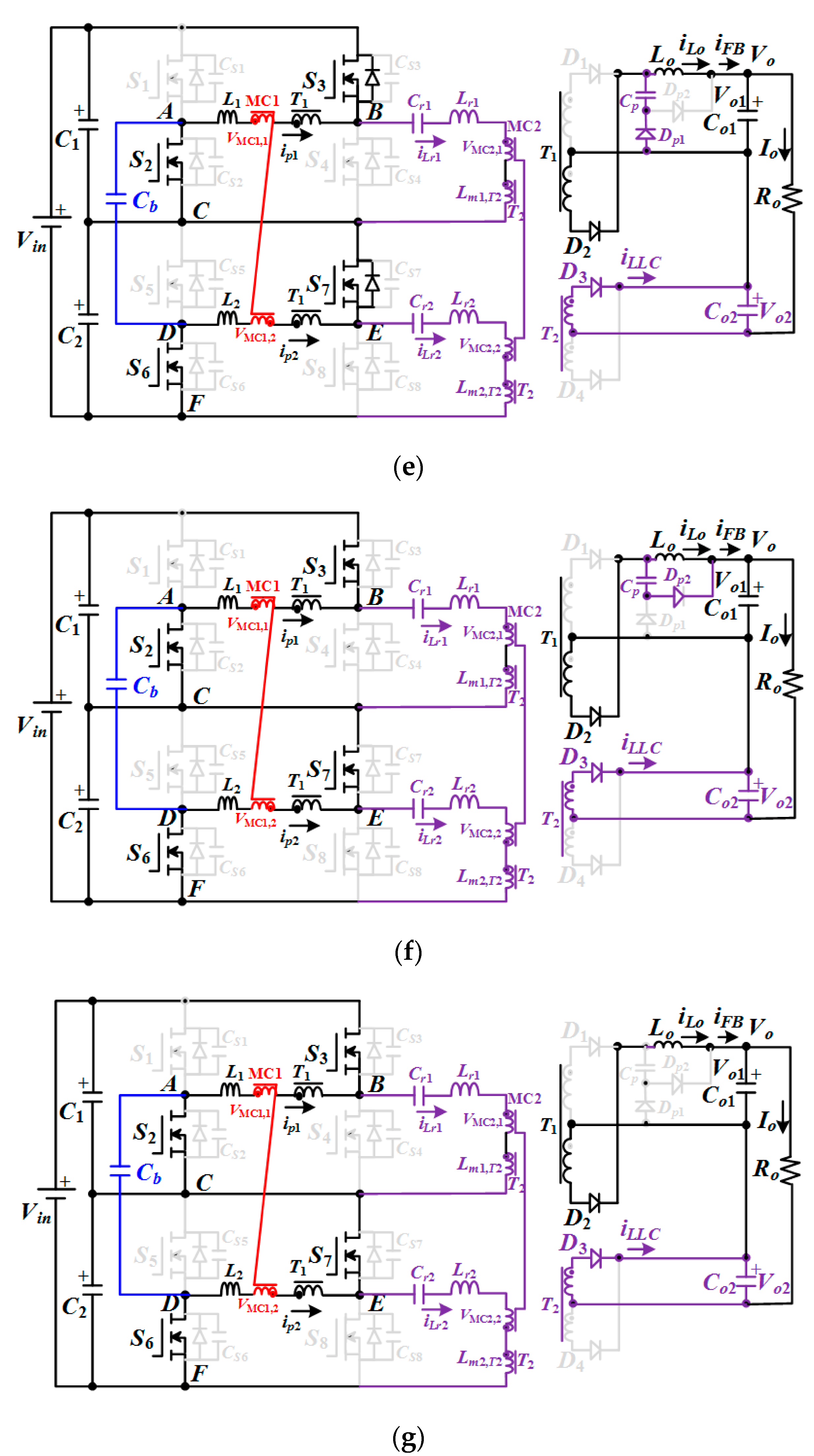
2. Circuit Diagram
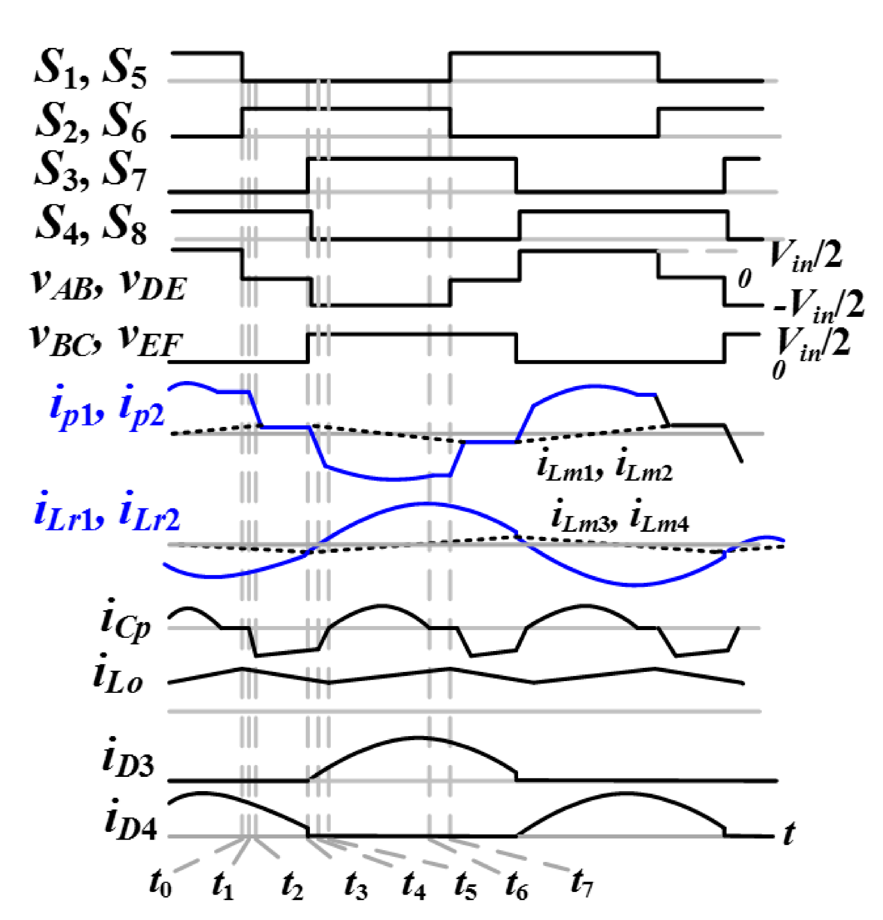
3. Principles of Operation
4. Circuit Analysis
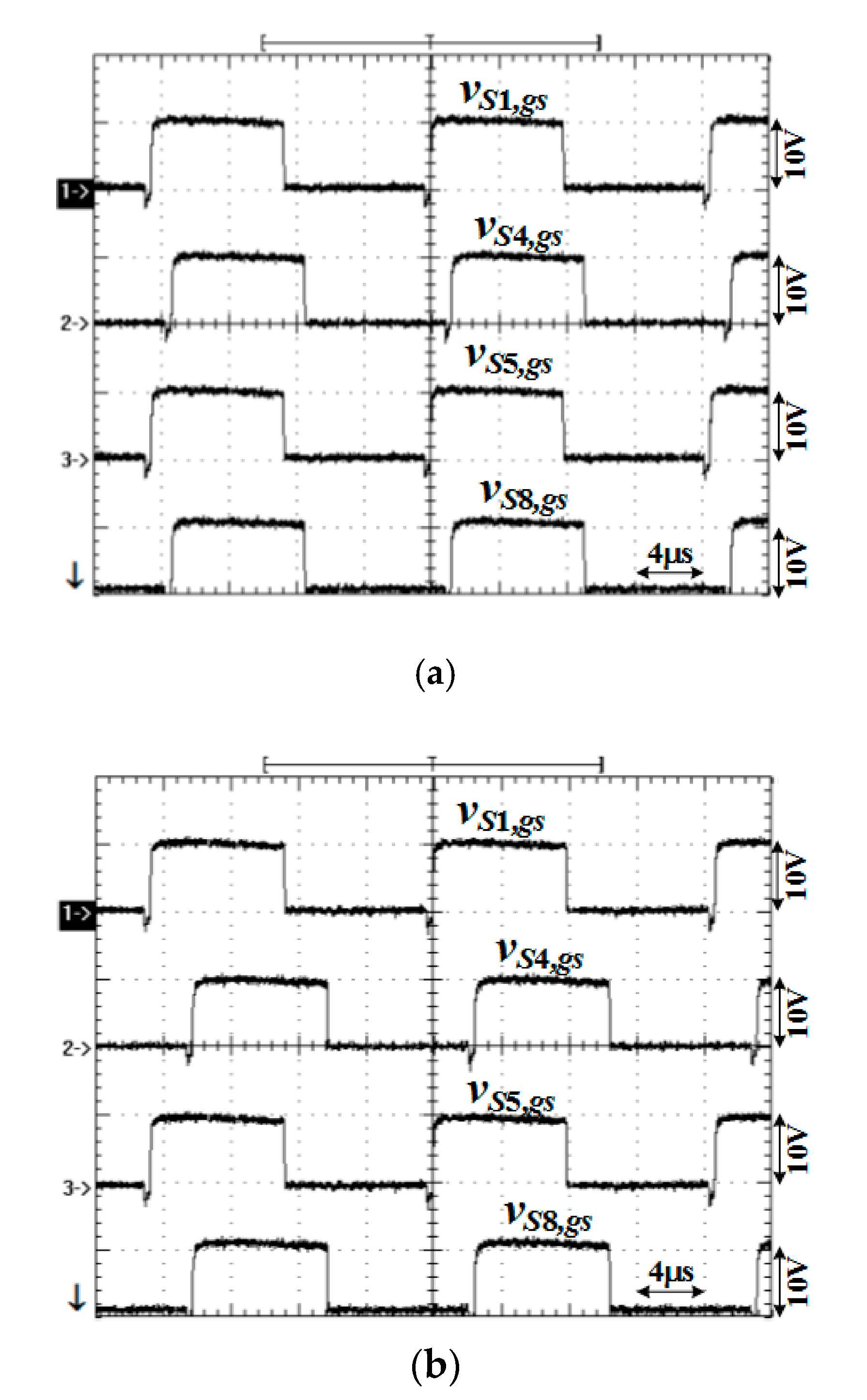
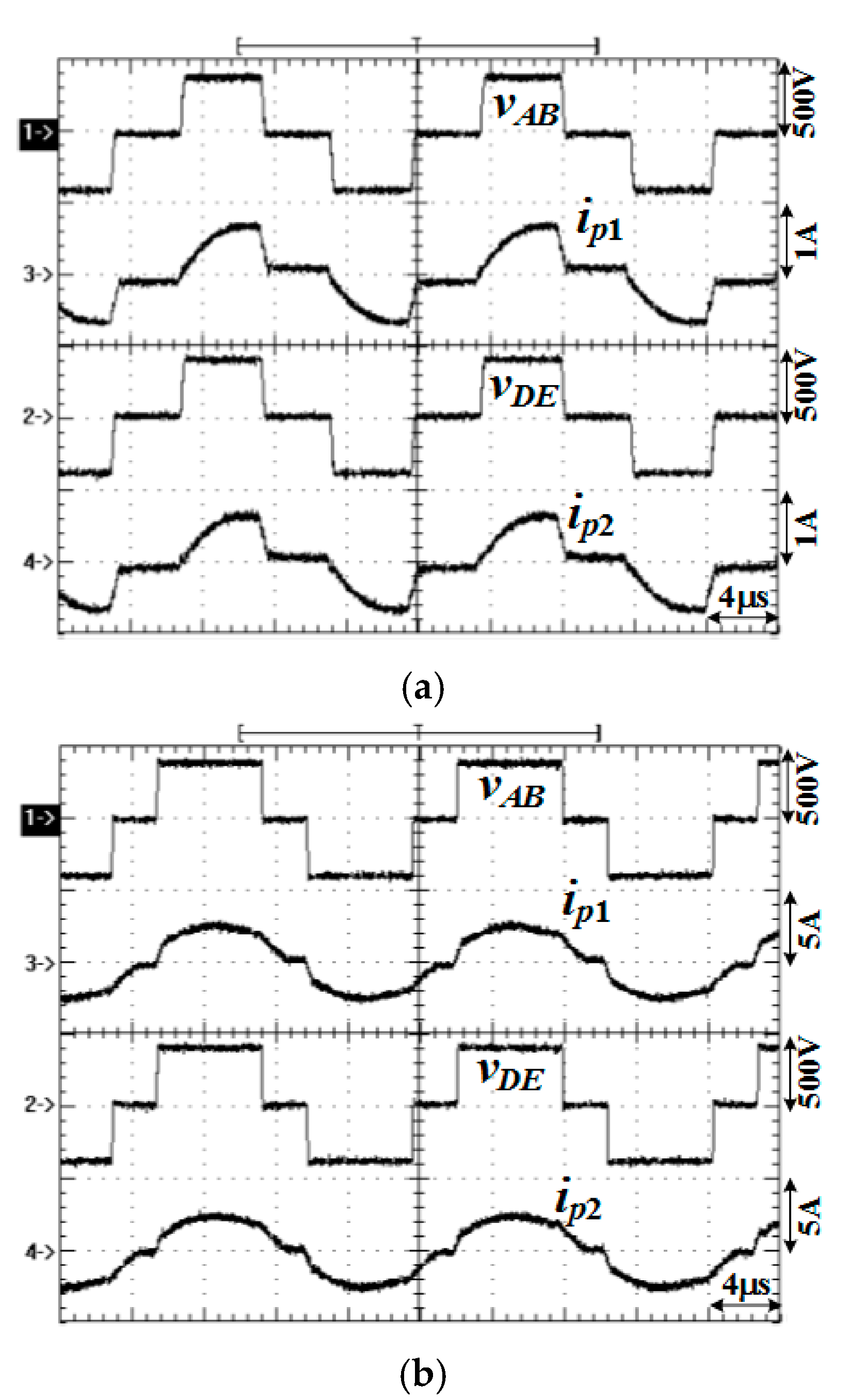
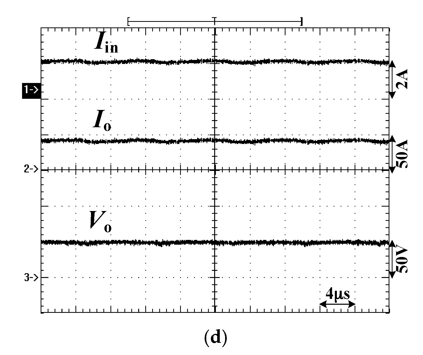
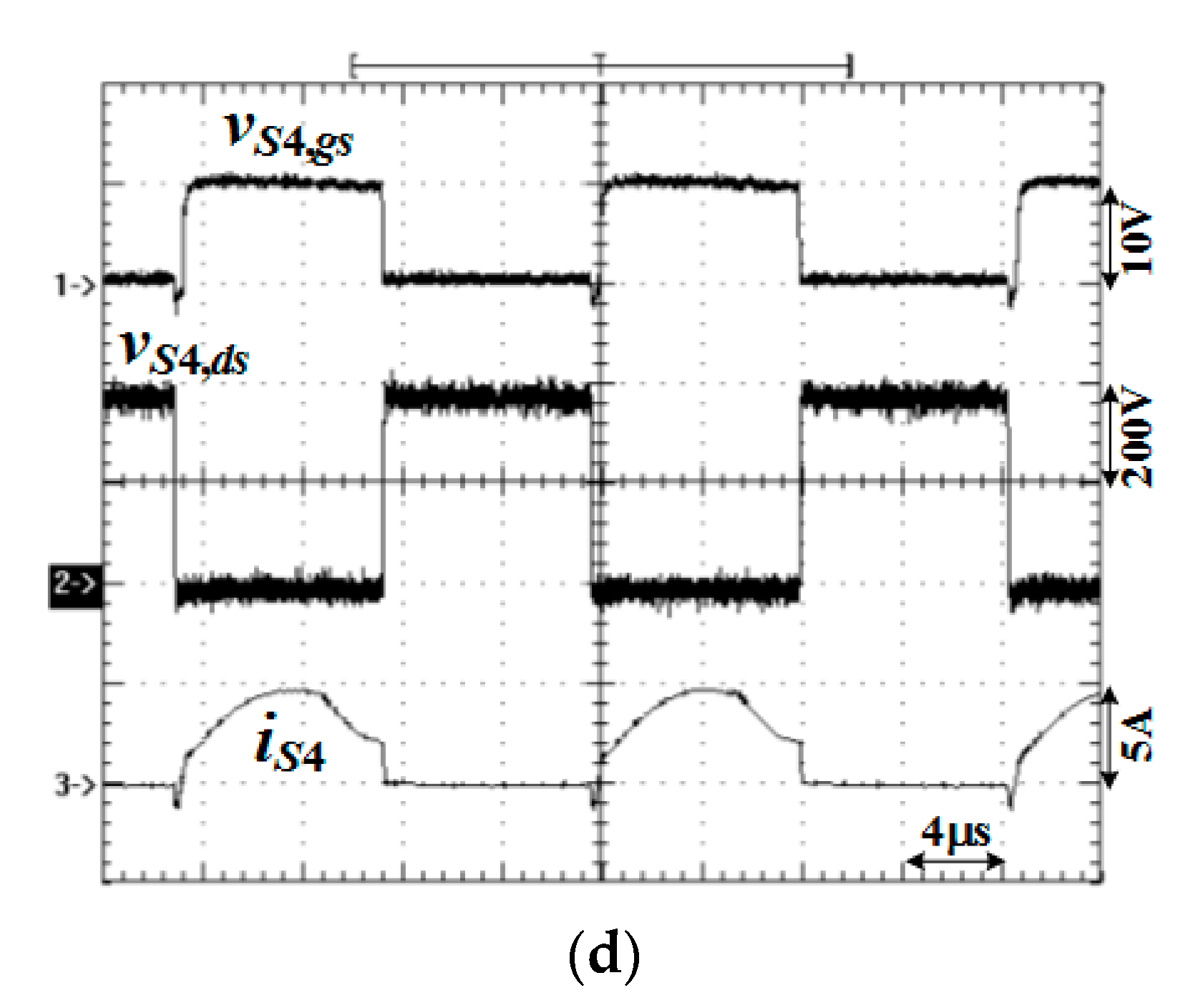
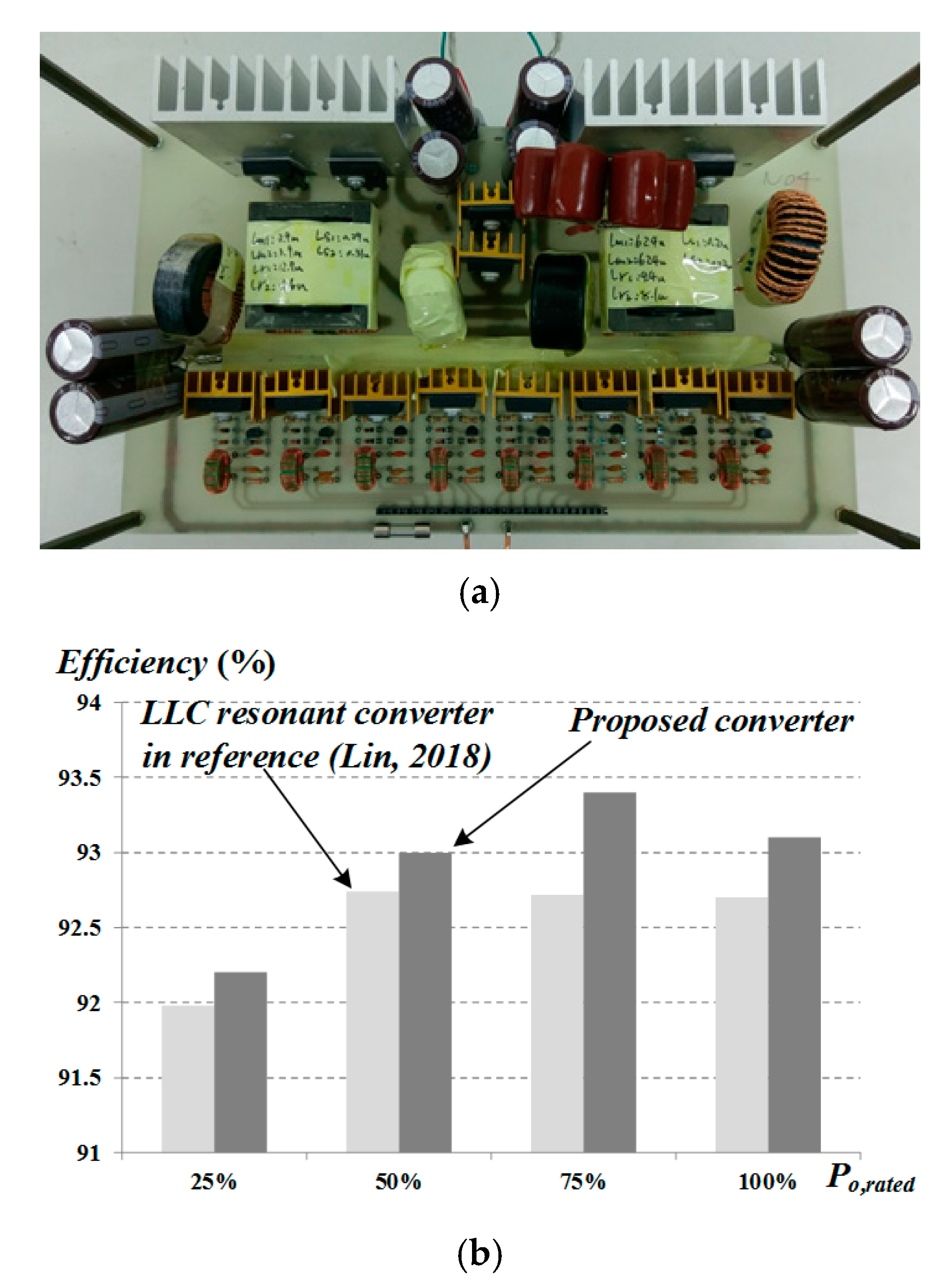
5. Design Considerations and Test Results
6. Conclusions
Author Contributions
Funding
Acknowledgments
Conflicts of Interest
References
- Song, B.M.; McDowell, R.; Bushnell, A.; Ennis, J. A three-level dc–dc converter with wide-input voltage operation for ship-electric power-distribution systems. IEEE Trans. Plasma Sci. 2004, 32, 1856–1863. [Google Scholar] [CrossRef]
- Fu, D.; Lee, F.C.; Qiu, Y.; Wang, F. A novel high-power-density three-level LCC resonant converter with constant-power-factor-control for charging applications. IEEE Trans. Power Electron. 2008, 23, 2411–2420. [Google Scholar] [CrossRef]
- Dragicevic, T.; Lu, X.; Vasquez, J.C.; Guerrero, J.M. DC microgrids—Part I: A review of power architectures, applications, and standardization issue. IEEE Trans. Power Electron. 2016, 31, 3528–3549. [Google Scholar] [CrossRef] [Green Version]
- Dragicevic, T.; Lu, X.; Vasquez, J.C. Guerrero, J.M. DC microgrids—Part II: A review of control strategies and stabilization techniques. IEEE Trans. Power Electron. 2016, 31, 4876–4891. [Google Scholar]
- Nejabatkhah, F.; Li, Y.W. Overview of power management strategies of hybrid AC/DC microgrid. IEEE Trans. Power Electron. 2015, 30, 7072–7089. [Google Scholar] [CrossRef]
- Lin, B.R. Soft switching resonant converter with duty-cycle control in DC micro-grid system. Int. J. Electron. 2018, 105, 137–152. [Google Scholar] [CrossRef]
- Chua, T.Z.Y.; Ong, Y.T.; Toh, C.L. Transformerless DC traction power conversion system design for light-rail-transit (LRT). In Proceedings of the 2017 IEEE Conference on Energy Conversion (CENCON), Kuala Lumpur, Malaysia, 30–31 October 2017; pp. 38–43. [Google Scholar]
- Han, S.K.; Moon, G.W.; Youn, M.J. A voltage-balanced phase-shifted three-level DC/DC converter operating from high-input voltage. IEEE Power Electron. Lett. 2003, 1, 74–77. [Google Scholar]
- Rodrigues, J.P.; Mussa, S.A.; Barbi, I.; Perin, A.J. Three-level zero-voltage switching pulse-width modulation DC-DC boost converter with active clamping. IET Proc. Power Electron. 2010, 3, 345–354. [Google Scholar] [CrossRef]
- Canales, F.; Barbosa, P.; Lee, F.C. A zero-voltage and zero-current switching three-level DC/DC converter. IEEE Trans. Power Electron. 2002, 17, 898–904. [Google Scholar] [CrossRef]
- Mishima, T.; Akamatsu, K.; Nakaoka, M. A high frequency-link secondary-side phase-shifted full-bridge soft-switching PWM DC-DC converter with ZCS active rectifier for EV battery charger. IEEE Trans. Power Electron. 2013, 28, 5758–5773. [Google Scholar] [CrossRef] [Green Version]
- Wu, X.; Zhang, J.; Xie, X.; Qian, Z. Analysis and optimal design considerations for an improved full-bridge ZVS dc-dc converter with high efficiency. IEEE Trans. Power Electron. 2006, 21, 1225–1233. [Google Scholar] [CrossRef]
- Chen, Y.; Kang, Y. An improved full-bridge dual-output dc–dc converter based on the extended complementary pulse width modulation concept. IEEE Trans. Power Electron. 2011, 26, 3215–3229. [Google Scholar] [CrossRef]
- Yu, W.; Lai, J.S.; Lai, W.H.; Wan, H. Hybrid resonant and PWM converter with high efficiency and full soft-switching range. IEEE Trans. Power Electron. 2012, 27, 4925–4933. [Google Scholar] [CrossRef]
- You, H.; Xu, C. A family of un-isolated modular dc/dc converters. In Proceedings of the 2016 IEEE 8th International Power Electronics and Motion Control Conference (IPEMC-ECCE Asia), Hefei, China, 22–26 May 2016; pp. 696–702. [Google Scholar]
- Liu, C.; Xu, X.; He, D.; Liu, H.; Tian, X.; Guo, Y.; Cai, G.; Ma, C.; Mu, G. Magnetic-coupling current-balancing cells based input-parallel output-parallel LLC resonant converter modules for high-frequency isolation of DC distribution systems. IEEE Trans. Power Electron. 2016, 31, 6968–6979. [Google Scholar] [CrossRef]
- Shi, J.J.; Liu, T.J.; Cheng, J.; He, X.N. Automatic current sharing of an input-parallel output-parallel (IPOP)-connected DC-DC converter system with chain-connected rectifiers. IEEE Trans. Power Electron. 2015, 30, 2997–3016. [Google Scholar] [CrossRef]


Publisher’s Note: MDPI stays neutral with regard to jurisdictional claims in published maps and institutional affiliations. |
© 2020 by the authors. Licensee MDPI, Basel, Switzerland. This article is an open access article distributed under the terms and conditions of the Creative Commons Attribution (CC BY) license (http://creativecommons.org/licenses/by/4.0/).
Share and Cite
Lin, B.-R.; Wu, G.-Y. Hybrid DC Converter with Current Sharing and Low Freewheeling Current Loss. Energies 2020, 13, 6631. https://doi.org/10.3390/en13246631
Lin B-R, Wu G-Y. Hybrid DC Converter with Current Sharing and Low Freewheeling Current Loss. Energies. 2020; 13(24):6631. https://doi.org/10.3390/en13246631
Chicago/Turabian StyleLin, Bor-Ren, and Guan-Yi Wu. 2020. "Hybrid DC Converter with Current Sharing and Low Freewheeling Current Loss" Energies 13, no. 24: 6631. https://doi.org/10.3390/en13246631