Abstract
This paper introduces a gallium nitride (GaN) high electron mobility transistor (HEMT)-based matrix converter for motor friendly drive systems. A fast switching characteristic of the GaN devices causes high dv/dt. This increases the importance of noise immunity and the reduction of parasitic components in system design. In addition, the high dv/dt in motor drive systems leads to voltage spike at a motor input terminal and leakage current through a motor chassis. Accordingly, a gate drive circuit consists of devices with a high common mode transient immunity. A printed circuit board was designed to minimize parasitic inductance, which was analyzed by performing simulations. To mitigate the dv/dt of the voltage applied to the motor and the leakage current, a dv/dt filter and a sine-wave filter were utilized as an output filter of the matrix converter. The effectiveness of each filter was verified by driving an induction motor.
1. Introduction
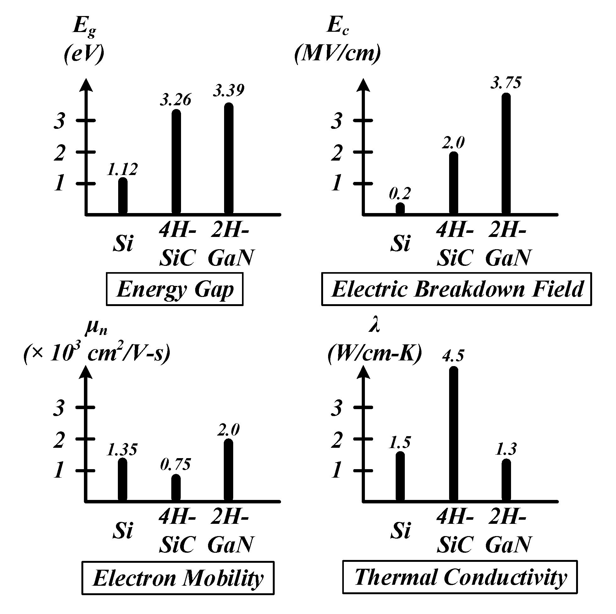
Wide bandgap (WBG) semiconductors like silicon carbide (SiC) metal oxide semiconductor field effect transistor (MOSFET) or gallium nitride (GaN) high electron mobility transistors (HEMTs) with high efficiency and a fast switching property have emerged as an alternative to silicon (Si) semiconductors in industry. WBG devices have superior characteristics than Si devices. Figure 1 shows the characteristics of Si, SiC, and GaN devices. GaN HEMT has the characteristics of high electric breakdown field, high thermal conductivity, and fast electron mobility [1,2,3]. A lateral two-dimensional electron gas (2DEG) channel has high electron mobility on AlGaN/GaN heteroepitaxy, which enables fast switching transients with a low capacitance property. To utilize these advantages, recently, AC motor drive systems with WBG devices have been studied [4,5,6,7,8,9,10,11]. In ref. [4], electro-hydrostatic actuators with high performance are applied to the WBG-based integrated motor drive. In refs. [6,8], the designs of GaN-based integrated modular motor drive systems are introduced. The fabricated system has a power density of 0.71 kW/L, drive efficiency of 98 %, and motor efficiency of 96.6 % [8]. The factors that degrade the switching properties of SiC devices in pulse-width modulation (PWM) inverter-fed induction motor drive are presented in [9], and the phenomenon of shaft voltage rising due to fast switching is studied in [11].
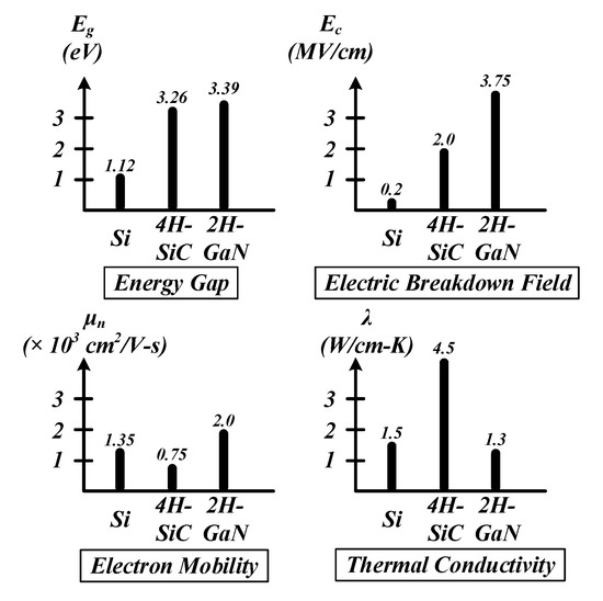
Figure 1.
Electrical properties of Si, 4H-SiC, 2H-gallium nitride (GaN).
As cited in the previous papers, many problems arise when the WBG devices are applied to motor drive systems. Especially, the dv/dt problem makes it difficult to safely operate a stable system because of fast switching transients. High dv/dt in motor drive systems reduces the life of the motor and is a key factor generating electromagnetic interference (EMI). When the dv/dt occurs, a common mode (CM) voltage is formed and the current through the motor bearings can reduce the life of the bearings. Similarly, the common mode current flowing through the ground line causes common mode EMI. In the case of WBG devices, the large magnitude of EMI can cause noises and interferences in the system. To solve this problem, a method of directly changing the motor structure is presented in [12].
Common mode voltage generates electromagnetic coupling between the stator windings and rotor windings. Electromagnetic shielding slot wedge is applied between the stator winding and the rotor winding to form an electromagnetic shield layer that decreases the current flow to the bearings.
The way to reduce the dv/dt without directly changing the motor structure is to use filters in the motor drive systems [13,14,15,16,17,18,19,20,21,22,23,24,25,26,27,28,29,30,31,32]. Comparisons of the filter performance in Si-insulated gate bipolar transistor (IGBT)-based and SiC MOSFET-based motor drive systems are explained in [13,14,15,16]. The designs of EMI filters for eliminating common mode current are expressed in [17,18,19,20,21]. The sine-wave filter is applied to WBG-based motor drive systems to verify the filter performance in [24,25,26,27], and the dv/dt filter for high speed motor drive systems is studied in [22,23]. The novel filter structure, not a typical LC filter structure is proposed in [29,30,31,32].
Motor drive applications with conventional inverters have a back-to-back structure where two voltage source inverters (VSIs) share the same DC link which consists of capacitors of large volume. Matrix converter is a good alternative to the back-to-back architecture, which allows direct conversion of ac input voltage to ac output voltage and there are no DC link capacitors. The matrix converter for motor drive systems has been increasingly studied due to the advantages of bidirectional power transfer, adjustable input power factor, and reduced system size [33,34,35,36,37,38]. There are many studies on three-phase matrix converters using WBG devices. However, the researches mainly focus on SiC devices, not GaN devices. In [39], the bidirectional GaN device is fabricated and the matrix converter is operated to drive an induction motor of 0.4kW. The output filter of the LC filter is shown on the circuit in the paper, but the filter design process is not described, which makes it difficult to know the exact purpose of its use. The objective of this paper is to design the GaN-based matrix converter having reliability with high dv/dt caused by fast switching transients. This paper is organized as follows. In Section 2, the designs of the gate driver circuit and power board for driving GaN HEMT. The design purpose of the gate driver circuit is to have immunity for dv/dt and a stable gate driving capability. Layout is performed to minimize the interference between the power loop and the gate loop. The parasitic inductances between the gate driver circuit and the source of the GaN HEMT are estimated using the Q3D Extractor. In Section 3, the dv/dt filter and sine-wave filter are introduced as output filters for motor drive applications to reduce high dv/dt at the motor input terminal. In Section 4, the switching performance of GaN HEMT on the fabricated printed circuit board (PCB) is tested. The experimental results, according to the output filter type, are compared. Finally, Section 5 summarizes the matrix converter design for GaN HEMT in motor drive systems.
2. Design and Practical Implementation for GaN-Based Power System
Since the GaN device has lower input capacitance, gate charge, and output capacitance than super junction MOSFET. It is possible to achieve hundreds of kV/μs fast switching transients. However, the CM current caused by the dv/dt can flow through parasitic inductance and capacitance within the devices and PCB patterns, which produces high spike voltage and noise. This can cause a malfunction of gate drivers, sensors, and microprocessors [40]. For proper design at high dv/dt, the devices with high common-mode transient immunity (CMTI) should be selected. Also, the layout should be carried out to minimize the effects of parasitic inductance. Then, parasitic inductance extraction was carried out, and the results are analyzed.
2.1. Design of Gate Driver Circuit
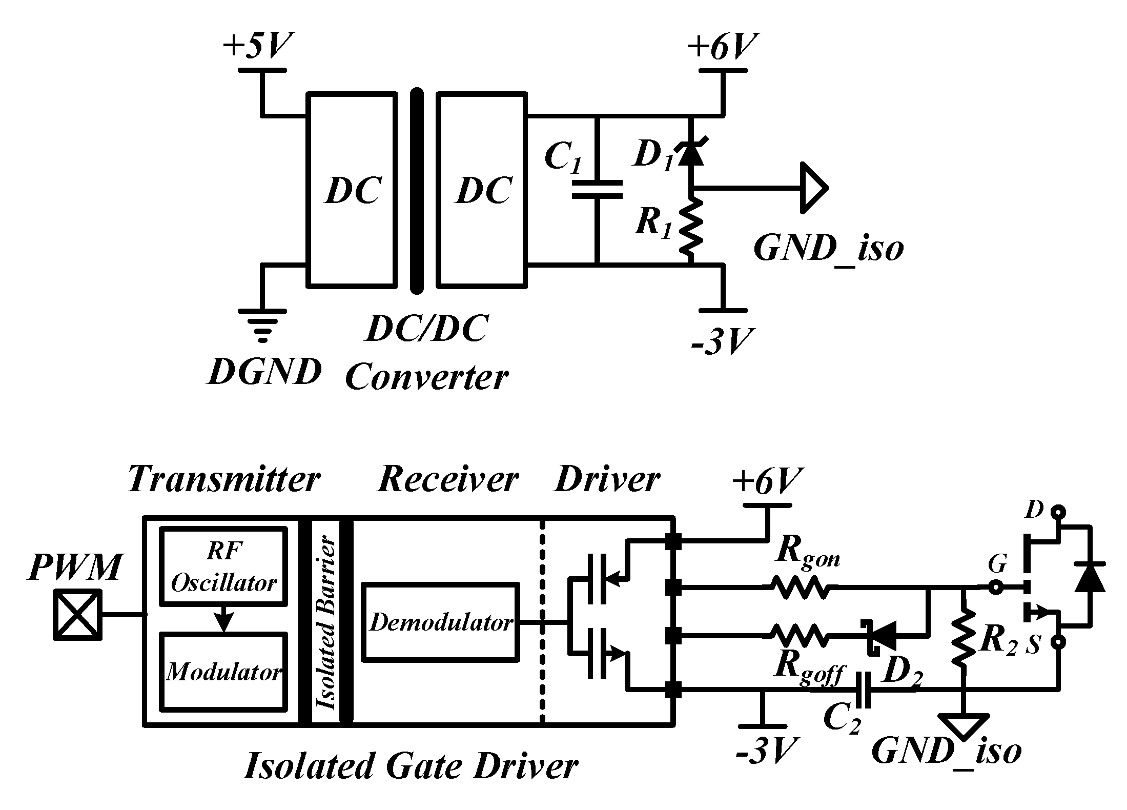
Figure 2 shows the schematic of the proposed gate driver circuit for GaN HEMT. The DC/DC converter is an insulated regulator with +9 V single output and 1 W. Because of a low inter-winding capacitance between input and output of the DC/DC converter, it is possible to reduce the CM current flowing through the inter-winding capacitor during short transients. Therefore, the corresponding gate driver circuit can achieve high CMTI capability. For a gate driver, a Si827x series from Silicon Labs is used. The gate driver is a digital insulated driver. The input signal modulates the carrier provided by an RF oscillator using an on/off keying method providing a superior noise immunity and immunity to magnetic fields. It also has the smallest input capacitance among the operating method of the gate driver such as optocouplers, magnetic couplers, capacitive couplers, etc. The gate driver has a CMTI of 200 kV/μs, and coupling capacitance of 0.5 pF, which allows the gate driver circuit to have the immunity against high dv/dt.

Figure 2.
Proposed gate driver schematic for GaN high electron mobility transistor (HEMT).
To assure the stability of the gate driver circuit, an unwanted turn-on phenomenon occurred by a miller effect should be prevented. For this purpose, a gate current path with a low impedance must be secured at turn-off. The selected gate driver has dual outputs and can be divided into on-current path and off-current path so that the impedance can be adjusted by altering the gate resistor at each path. The appropriate ratio of the gate on and gate off resistance can ensure the stability of the gate driver. It is recommended that the ratio is selected as between 5 and 10 according to [41]. In addition, the parasitic inductances in the gate driver circuit are one of the main factors affecting the stability of the gate driver. The gate inductance (Lg), common source inductance (Lcs) are the key components that cause ringing and overshoot on gate-source voltage. If the values are large, the oscillation problem can lead to damage to the devices. Minimizing parasitic inductance in the gate driver circuit should be achieved through the appropriate PCB layout design.
2.2. Design of PCB Layout
To fabricate the designed gate driver circuit and power board circuit, the PCB layout was carried out using Altium software. Bidirectional GaN HEMT switches are configured by a common source structure. For the PCB layout, it is important to minimize the parasitic inductances such as gate loop inductance, common source inductance, and power loop inductance in layout. The GaN HEMT device used in this paper has a package without a wire bond. Compared to TO-247 switches having a package source inductance values of about 10 to 15 nH resulting from long lead length, the GaN HEMT device has a value of about 0.05 nH. This is a very small inductance value, which has a highly large advantage in GaN HEMT operation and can minimize the impact of parasitic inductance. In order to reduce the gate loop inductance, the gate driver is placed close to the gate of GaN HEMT device, and low inductance is secured by using coppers instead of wiring with the trace. To reduce source inductance (Ls) between the bidirectional GaN HEMT switches, a vertical power loop was used [42]. This structure diminishes interference between the gate loop path and the power loop path and makes the value of Ls low. Unlike the typical method of placing the switches in a lateral structure on the same layer as shown in Figure 3a, one switch is placed in the top layer and the other in the bottom layer like Figure 3b. In the lateral structure, the gate loop and the power loop are parallel, which is sensitive to magnetic noise interference. However, the vertical structure can minimize coupling between the gate loop and the power loop. By employing this structure, the inductance between switches is limited only by the package inductance and size of the device, and PCB thickness. The paths among sources of each switching device are connected through multiple vias, which can obtain a low value of Ls.

Figure 3.
(a) Lateral structure of GaN HEMT; (b) vertical structure of GaN HEMT.
2.3. Estimation of Parasitic Inductance
To analyze whether the designed PCB has a minimum parasitic inductance, a Finite-Element Analysis (FEA) was conducted using ANSYS Electronics software. The sources of a bidirectional switch are connected through several vias as shown in Figure 4a. AC resistance and AC inductance can be obtained at various solution frequency conditions using a Q3D extractor. The analysis result yields a Ls of 1.5 pH for one bi-directional switch, which proves that the vertical loop design can have low source inductance. Similarly, the gate loop inductance is analyzed through the FEA. In this paper, the parasitic inductance of the gate-off current path is estimated at 10 kHz as shown in Figure 4b. The estimated inductance is 4.32 nH, which means that the designed gate driver has enough reliability to drive the GaN HEMT devices.

Figure 4.
(a) Gate driver circuit of fabricated printed circuit board (PCB); (b) ANSYS Q3D software view.
3. Output Filter Design
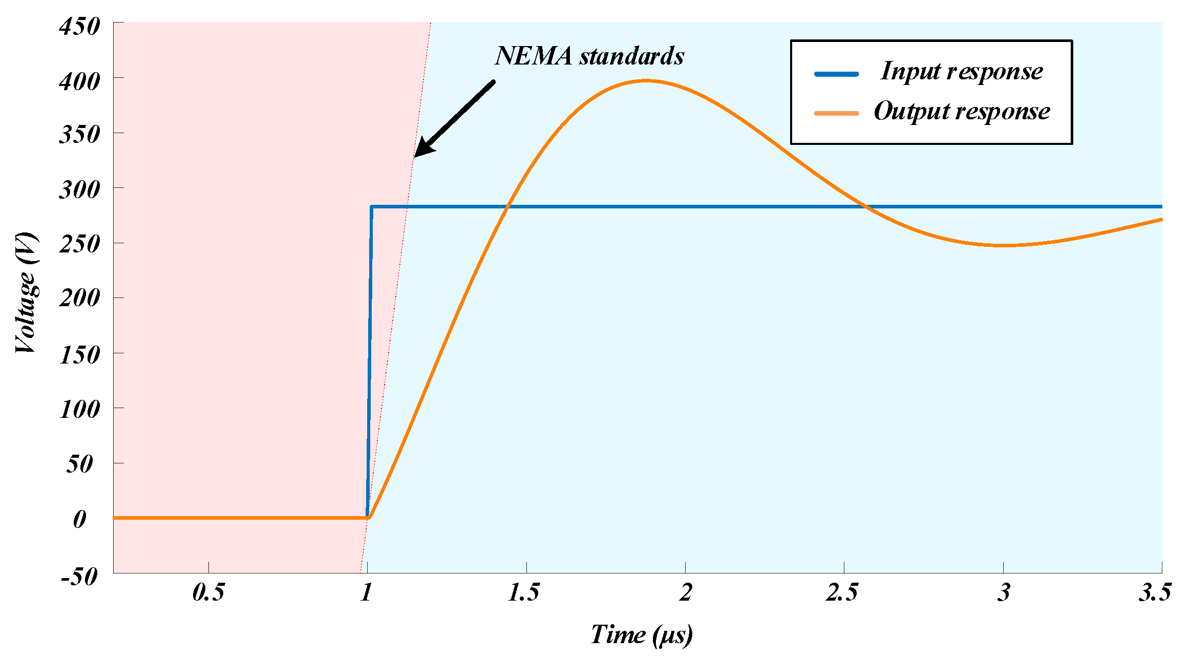
Table 1 shows specifications associated with dv/dt in national electrical manufacturers association (NEMA) standards [43]. The specifications limit the maximum voltage and the rise time at the motor input terminal to ensure a stable motor drive. The rise time of the GaN HEMT utilized in this paper was 12.4 ns, so if the dv/dt is not mitigated by the output filter or gate resistance, then the minimum rise time in standards is not satisfied. Therefore, to alleviate high dv/dt, dv/dt filter and sine-wave filter were applied as an output filter, respectively. The output filters are shown in Figure 5, and the transfer functions of output filters are as follows:

Table 1.
National electrical manufacturers association (NEMA) dv/dt standards.
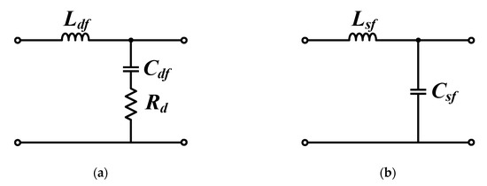
Figure 5.
Output filter circuit; (a) for dv/dt filter; (b) for sine-wave filter.
The resonant frequency of each filter is calculated as below:
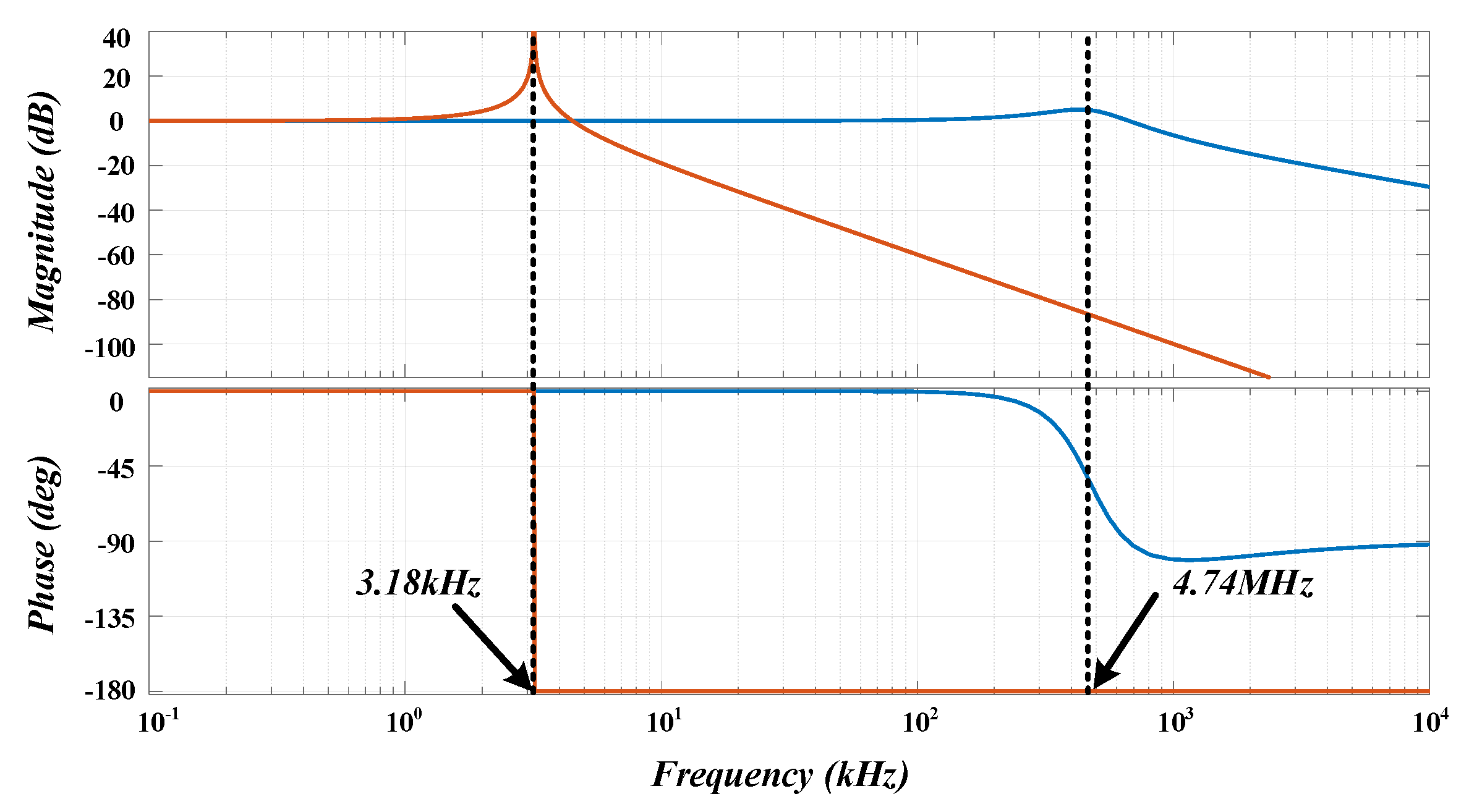
where fsine is the resonant frequency of the sine-wave filter and fdvdt is the resonant frequency of the dv/dt filter. The resonant frequency is determined in the same way by the inductance and capacitance in each filter. However, depending on the purpose of each filter, the resonant frequencies are located at different boundaries. The resonant frequency of the sine-wave filter should be within the range of greater than the fundamental frequency and less than the switching frequency. The sine-wave filter attenuates the switching frequency components of the output voltage. So, since the sinusoidal voltage with fundamental frequency is applied to the motor, problems by high dv/dt are mitigated. On the other hand, the purpose of the dv/dt filter is to limit the rise time of the voltage applied to the motor input terminal. The minimum rise time in the standard is 0.1 μs, so the resonant frequency of dv/dt filter should be within the range of greater than the switching frequency and less than 10 MHz [31].
Table 2 shows the parameters of the designed output filter. The frequency response of each output filter is illustrated in Figure 6. As shown in Figure 6, the resonant frequency of each output filter is located within the above frequency constraints. Figure 7 shows the output voltages of the matrix converter and the dv/dt filter. The magnitude of the output voltage is considered as the peak value of the input line-to-line voltage, which is the maximum value that the matrix converter can generate. The designed dv/dt filter enables the matrix converter to meet the specification in Table 2.

Table 2.
Output filter parameters.

Figure 6.
Bode plot of dv/dt filter and sine-wave filter (red line: sine-wave filter, blue line: dv/dt filter).
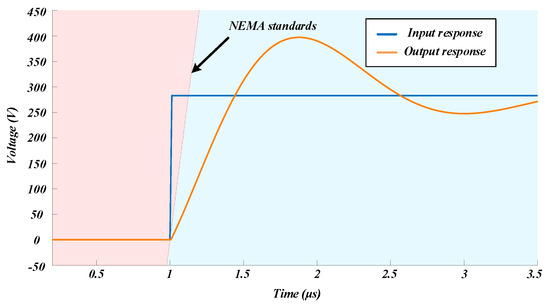
Figure 7.
Time response graph considering real input signal.
4. Experimental Results
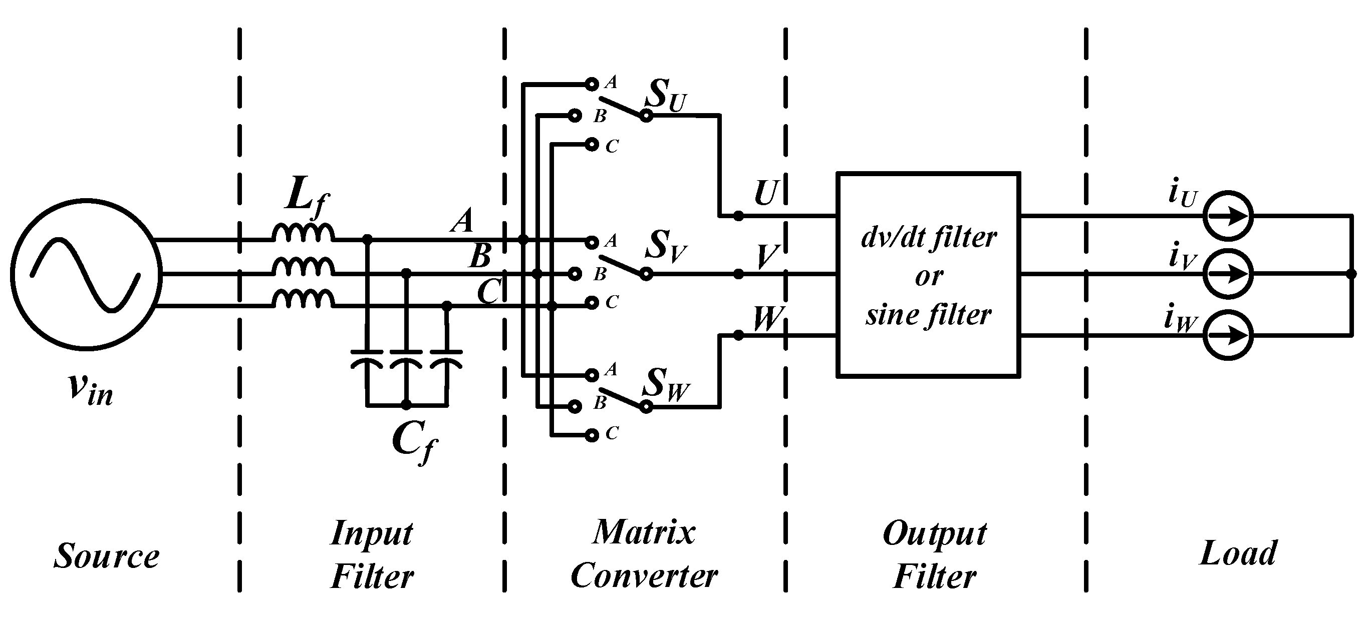
Figure 8 shows the schematic of the direct matrix converter. A normally-off enhancement-mode 650 V GaN HEMT (GS66516T, GaN Systems) is used in this paper [44]. To implement a modulation algorithm, the input line-to-line voltages were measured by using LV-25P from LEM, and the control board equipped with a microcontroller, TMS320F28377S from Texas Instrument, was used. The experimental electrical specifications are described in Table 3.
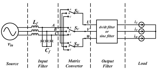
Figure 8.
Schematic of matrix converter system.

Table 3.
Experimental electrical specifications.
4.1. Switching Performance
The experiments for evaluating switching performances of the fabricated matrix converter are carried out. Since the switching characteristics in drain-source voltage can be degraded in induction motor drives [9], the switching performance experiment is carried out in resistive load conditions. Figure 9 shows the gate-source voltage and the drain-source voltage at turn-on of GaN HEMT and turn-off of GaN HEMT respectively. The rise time of the gate-source voltage is 5.9 ns, and the fall time is 5.4 ns. The rise time of the drain-source voltage is 194.2 ns, and the fall time of the drain-source voltage is 10.4 ns. While very fast switching transients are possible in gate-source voltage, the rise time of the drain-source voltage is considerably large. This may occur because the power loop inductance, except for the source inductance between the GaN HEMT switches, has not been considered in the entire design procedures. This phenomenon needs be improved in future work to make correct turn-off operation.

Figure 9.
Switching waveform of GaN HEMT in matrix converter; (a) at turn-on of GaN HEMT; and (b) at turn-off of GaN HEMT.
4.2. Output Filter Experiments
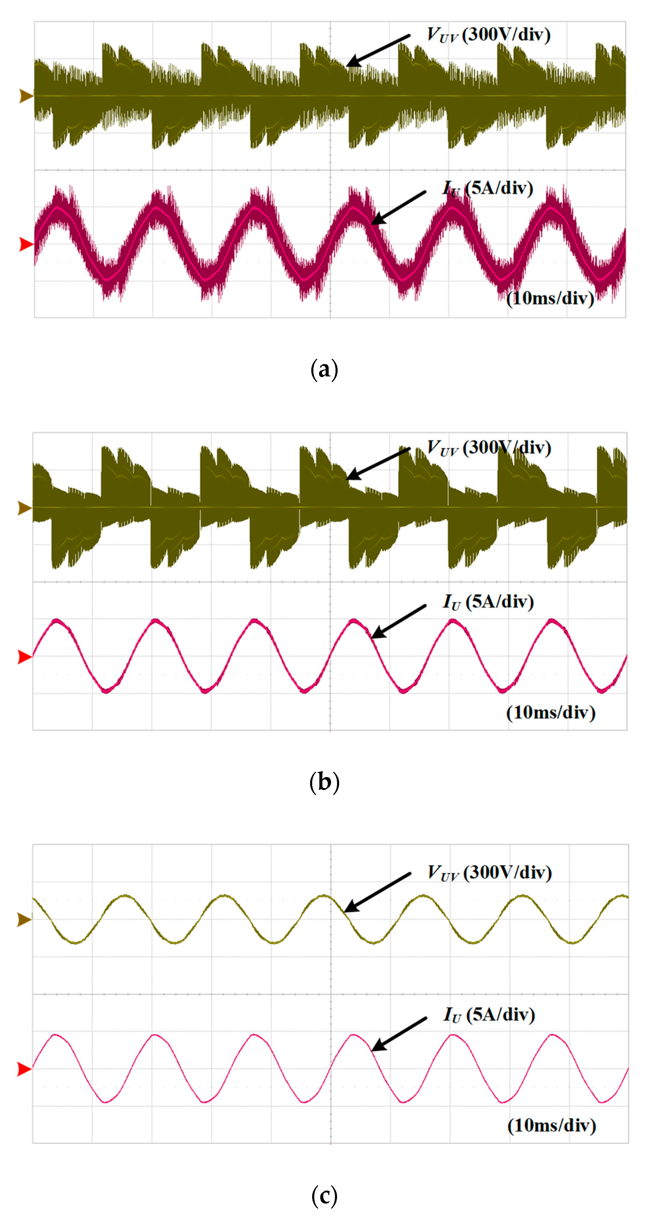
For the GaN-based matrix converter in motor drive system, the dv/dt filter and the sine-wave filter have been established for experimental validation of the performance analysis. Figure 10 shows the experimental results of the matrix converter without and with the different output filters, where VUV is the line-to-line terminal voltage of the induction motor, and IU is the motor current in phase U. The case without any filter can be observed in Figure 10a. When the output filter is not adopted in the GaN-based matrix converter, the input quality of VUV and IU has high-frequency components above the switching frequency of 10 kHz in the steady-state. In the case of the dv/dt filter, the high-frequency components of the motor input current are considerably reduced, although the line-to-line terminal voltage still has high-frequency components as Figure 10b. As shown in Figure 10c where the sine-wave filter is adopted, a pure sinusoidal waveform of VUV and IU without the high-frequency harmonics could be observed as expected. Here, it is clear that the output filters reduce the voltage stress of the motor drive system, but the detailed performance comparison of the output filters can be discussed with the common mode current which is given in the following section.
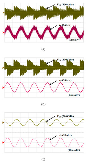
Figure 10.
Experimental results of matrix converter in induction load; (a) without output filter; (b) with dv/dt filter; and (c) with sine-wave filter.
Figure 11 shows the line-to-line voltage at the induction motor input terminal of the GaN-based matrix converter without and with the dv/dt filter. As shown in Figure 11a, it has high-frequency voltage ringing and high dv/dt spikes due to the fast rise time of the GaN devices where the rise time is 78 ns. However, as shown in Figure 11b, the rise time of 0.1 μs by NEMA standards can be satisfied with the designed dv/dt filter where the rise time is 478 ns. It shows that the dv/dt filter significantly mitigates the high-frequency ringing components at the motor terminal.

Figure 11.
Experimental results of line-to-line voltage in motor input terminal in the case of (a) without output filter; and (b) with dv/dt filter.
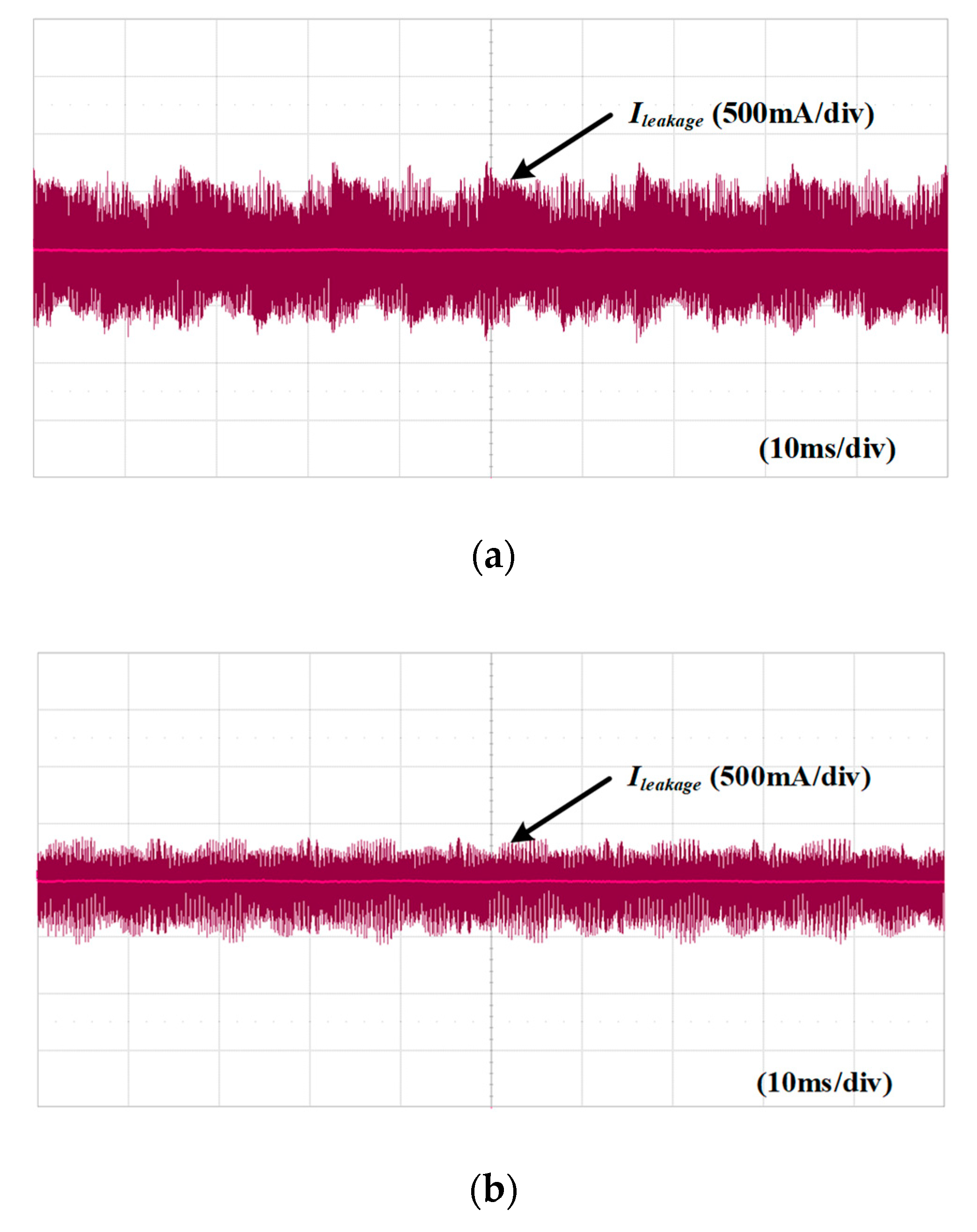
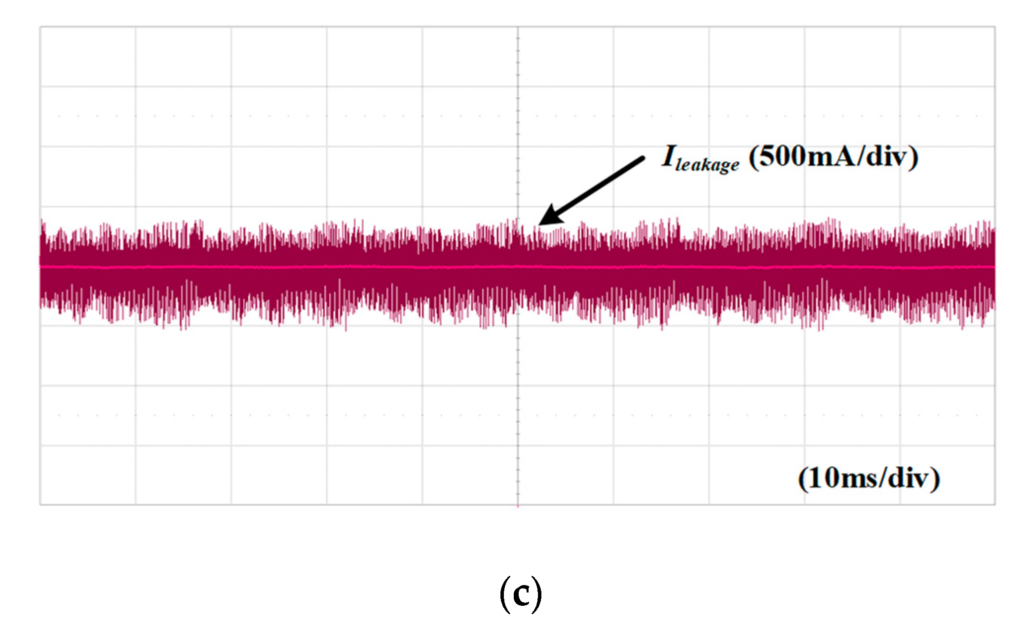
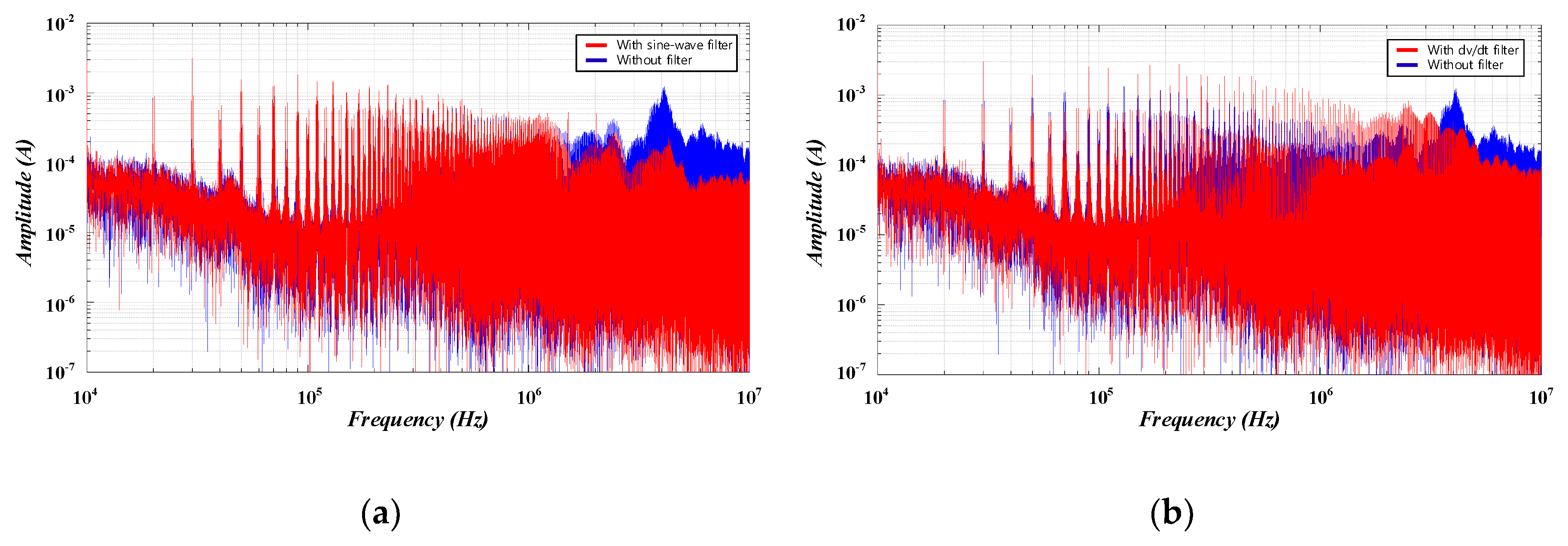
Figure 12 shows the common mode current measurement results of the GaN-based matrix converter according to the various output filter options. The common mode current considerably decreases by using the output filters. For the detailed analysis, the frequency spectrums without and with the output filters is obtained in Figure 13. The magnitude of the common mode current is reduced by the sine-wave filter in the frequency range from 1.5 MHz to 10 MHz.
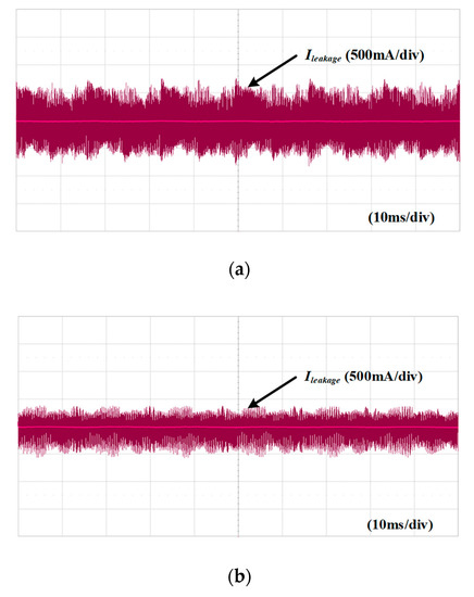
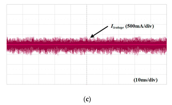
Figure 12.
Experimental results of leakage current in time scale; (a) without output filter; (b) with dv/dt filter; and (c) with sine-wave filter.

Figure 13.
(a) Common mode current spectrum without or with sine-wave filter; and (b) Common mode current spectrum without or with dv/dt filter.
Meanwhile, in the case of the dv/dt filter, the common mode current amplitude slightly decreases in the frequency range from 3.5 MHz to 10 MHz. From the frequency spectrum results, it is confirmed that the sine-wave filter has better mitigation performance for the common mode current due to its pure sine-wave voltage on the input motor terminal.
5. Conclusions
In this paper, a design of the GaN-based matrix converter was suggested to obtain a robustness for high dv/dt. The gate driver circuit was designed for high CMTI and reliable operation of the GaN HEMT. PCB layout was also designed to minimize parasitic inductance and interference between the digital loop and the power loop, leading to the remarkable results from the parasitic inductance of the gate path and source path. It was confirmed that NEMA standards were satisfied by applying the dv/dt filter and sine-wave filter. With the dv/dt filter, the experimental result shows that the rise time of line-to-line voltage in motor input terminal is 478 ns above 0.1 μs. With the sine-wave filter, the closely pure sinusoidal output voltage and current waveforms were obtained to meet the rated magnitude and frequency without any harmonic components. Finally, CM current according to each output filter was compared. The magnitude of CM current was decreased by about 47% when the output filters were applied compared to the absence of the output filters. The CM current spectrum results show that the output filters are effective at MHz frequency band and the sine-wave filter can reduce the CM current more than the dv/dt filter. Based on the results of the experiments, the dv/dt filter is suitable when the NEMA standards should be considered and the sine-wave filter is suitable when the CM current reduction should be considered preferentially.
Author Contributions
H.B. implemented the system and performed the experiments. Y.C. managed the project. All authors have read and agreed to the published version of the manuscript.
Funding
This work was supported by the National Research Foundation of Korea (NRF) grant funded by the Korea government (MSIT). (No. 2017R1C1B2009425). This work was supported by “Human Resources Program in Energy Technology” of the Korea Institute of Energy Technology Evaluation and Planning (KETEP), granted financial resource from the Ministry of Trade, Industry and Energy, Republic of Korea. (No. 20194030202370).
Conflicts of Interest
The authors declare no conflict of interest.
References
- Chen, K.J.; Häberlen, O.; Lidow, A.; Lin Tsai, C.; Ueda, T.; Uemoto, Y.; Wu, Y. GaN-on-Si Power Technology: Devices and Applications. IEEE Trans. Ind. Electron. 2017, 64, 779–795. [Google Scholar] [CrossRef]
- Jones, E.A.; Wang, F.F.; Costinett, D. Review of Commercial GaN Power Devices and GaN-Based Converter Design Challenges. IEEE Trans. Emerg. Sel. Top. Power Electron. 2016, 4, 707–719. [Google Scholar] [CrossRef]
- Chow, T.P. Wide bandgap semiconductor power devices for energy efficient systems. In Proceedings of the 2015 IEEE 3rd Workshop on Wide Bandgap Power Devices and Applications (WiPDA), Blacksburg, VA, USA, 2–4 November 2015; pp. 402–405. [Google Scholar]
- Lee, W.; Li, S.; Han, D.; Sarlioglu, B.; Minav, T.A.; Pietola, M. A Review of Integrated Motor Drive and Wide-Bandgap Power Electronics for High-Performance Electro-Hydrostatic Actuators. IEEE Trans. Transport. Electrif. 2018, 4, 684–693. [Google Scholar] [CrossRef]
- Morya, A.K.; Gardner, M.C.; Anvari, B.; Liu, L.; Yepes, A.G.; Doval-Gandoy, J.; Toliyat, H.A. Wide Bandgap Devices in AC Electric Drives: Opportunities and Challenges. IEEE Trans. Transport. Electrif. 2019, 5, 3–20. [Google Scholar] [CrossRef]
- Wang, J.; Li, Y.; Han, Y. Integrated Modular Motor Drive Design with GaN Power FETs. IEEE Trans. Ind. Appl. 2015, 51, 3198–3207. [Google Scholar] [CrossRef]
- Ding, X.; Zhou, Y.; Cheng, J. A review of gallium nitride power device and its applications in motor drive. CES Trans. Electr. Mach. Syst. 2019, 3, 54–64. [Google Scholar] [CrossRef]
- Uğur, M.; Keysan, O. Multi-physics design optimisation of a GaN-based integrated modular motor drive system. J. Eng. 2019, 2019, 3900–3905. [Google Scholar]
- Zhang, Z.; Wang, F.; Tolbert, L.M.; Blalock, B.J.; Costinett, D.J. Evaluation of Switching Performance of SiC Devices in PWM Inverter-Fed Induction Motor Drives. IEEE Trans. Power Electron. 2015, 30, 5701–5711. [Google Scholar] [CrossRef]
- Marzoughi, A.; Burgos, R.; Boroyevich, D. Investigating Impact of Emerging Medium-Voltage SiC MOSFETs on Medium-Voltage High-Power Industrial Motor Drives. IEEE Trans. Emerg. Sel. Top. Power Electron. 2019, 7, 1371–1387. [Google Scholar] [CrossRef]
- Han, Y.; Lu, H.; Li, Y.; Chai, J. Analysis and Suppression of Shaft Voltage in SiC-Based Inverter for Electric Vehicle Applications. IEEE Trans. Power Electron. 2019, 34, 6276–6285. [Google Scholar] [CrossRef]
- Bai, B.; Wang, Y.; Wang, X. Suppression for Discharging Bearing Current in Variable-Frequency Motors Based on Electromagnetic Shielding Slot Wedge. IEEE Trans. Magn. 2015, 51, 1–4. [Google Scholar] [CrossRef]
- Swamy, M.M.; Kang, J.; Shirabe, K. Power Loss, System Efficiency, and Leakage Current Comparison between Si IGBT VFD and SiC FET VFD with Various Filtering Options. IEEE Trans. Ind. Appl. 2015, 3858–3866. [Google Scholar] [CrossRef]
- Shirabe, K.; Swamy, M.M.; Kang, J.; Hisatsune, M.; Wu, Y.; Kebort, D.; Honea, J. Efficiency Comparison Between Si-IGBT-Based Drive and GaN-Based Drive. IEEE Trans. Ind. Appl. 2014, 50, 566–572. [Google Scholar] [CrossRef]
- Gong, X.; Ferreira, J.A. Comparison and Reduction of Conducted EMI in SiC JFET and Si IGBT-Based Motor Drives. IEEE Trans. Power Electron. 2014, 50, 1757–1767. [Google Scholar] [CrossRef]
- Baek, S.; Cho, Y.; Cho, B.; Hong, C. Performance Comparison between Two-Level and Three-Level SiC-Based VFD Applications with Output Filters. IEEE Trans. Ind. Appl. 2019, 55, 4770–4779. [Google Scholar] [CrossRef]
- Ala, G.; Giaconia, G.C.; Giglia, G.; Piazza, M.C.D.; Vitale, G. Design and Performance Evaluation of a High Power-Density EMI Filter for PWM Inverter-Fed Induction-Motor Drives. IEEE Trans. Ind. Appl. 2016, 52, 2397–2404. [Google Scholar] [CrossRef]
- Wang, S.; Maillet, Y.Y.; Wang, F.; Boroyevich, D.; Burgos, R. Investigation of Hybrid EMI Filters for Common-Mode EMI Suppression in a Motor Drive System. IEEE Trans. Power Electron. 2010, 25, 1034–1045. [Google Scholar] [CrossRef]
- Akagi, H.; Shimizu, T. Attenuation of Conducted EMI Emissions from an Inverter-Driven Motor. IEEE Trans. Power Electron. 2008, 23, 282–290. [Google Scholar] [CrossRef]
- Akagi, H.; Tamura, S. A Passive EMI Filter for Eliminating Both Bearing Current and Ground Leakage Current From an Inverter-Driven Motor. IEEE Trans. Power Electron. 2006, 21, 1459–1469. [Google Scholar] [CrossRef]
- Han, D.; Li, S.; Wu, Y.; Choi, W.; Sarlioglu, B. Comparative Analysis on Conducted CM EMI Emission of Motor Drives: WBG Versus Si Devices. IEEE Trans. Ind. Electron. 2017, 64, 8353–8363. [Google Scholar] [CrossRef]
- Kim, H.; Acharya, S.; Anurag, A.; Kim, B.; Bhattacharya, S. Effect of Inverter Output dv/dt with Respect to Gate Resistance and Loss Comparison with dv/dt Filters for SiC MOSFET based High Speed Machine Drive Applications. In Proceedings of the 2019 IEEE Energy Conversion Congress and Exposition (ECCE), Baltimore, MD, USA, 29 September–3 October 2019; pp. 2301–2306. [Google Scholar]
- Kim, H.; Kim, B.; Bhattacharya, S. An Analytical Design Strategy and Implementation of a Dv/Dt Filter for WBG Devices Based High Speed Machine Drives. In Proceedings of the IECON 2018-44th Annual Conference of the IEEE Industrial Electronics Society, Washington, DC, USA, 21–23 October 2018; pp. 385–390. [Google Scholar]
- Stubenrauch, F.; Seliger, N.; Schmitt-Landsiedel, D. Design and Performance of a 200 kHz GaN Motor Inverter with Sine Wave Filter. In Proceedings of the PCIM Europe 2017; International Exhibition and Conference for Power Electronics, Intelligent Motion, Renewable Energy and Energy Management, Nuremberg, Germany, 16–18 May 2017; pp. 1–9. [Google Scholar]
- Müller, J.; Manthey, T.; Han, D.; Sarlioglu, B.; Friebe, J.; Mertens, A. Output Sine-Wave Filter Design and Characterization for a 10 kW SiC Inverter. In Proceedings of the 2019 IEEE Energy Conversion Congress and Exposition (ECCE), Baltimore, MD, USA, 29 September–3 October 2019; pp. 359–366. [Google Scholar]
- Maislinger, F.; Ertl, H.; Stojcic, G.; Holzner, F. Efficiency and Motor-Performance Improvement Using WBG-Inverters with Observer-based Actively Damped LC-Sine Wave Filters. In Proceedings of the PCIM Europe 2019; International Exhibition and Conference for Power Electronics, Intelligent Motion, Renewable Energy and Energy Management, Nuremberg, Germany, 7–9 May 2019; pp. 1–9. [Google Scholar]
- Maislinger, F.; Ertl, H.; Stojcic, G.; Lagler, C.; Holzner, F. Design of a 100 kHz wide bandgap inverter for motor applications with active damped sine wave filter. J. Eng. 2019, 17, 3766–3771. [Google Scholar] [CrossRef]
- Yuen, K.K.; Chung, H.S. A Low-Loss “RL-Plus-C” Filter for Overvoltage Suppression in Inverter-Fed Drive System With Long Motor Cable. IEEE Trans. Power Electron. 2015, 30, 2167–2181. [Google Scholar] [CrossRef]
- Velander, E.; Bohlin, G.; Sandberg, Å.; Wiik, T.; Botling, F.; Lindahl, M.; Zanuso, G.; Nee, H. An Ultralow Loss Inductorless $dv/dt$ Filter Concept for Medium-Power Voltage Source Motor Drive Converters with SiC Devices. IEEE Trans. Power Electron. 2018, 33, 6072–6081. [Google Scholar] [CrossRef]
- Schroedermeier, A.; Ludois, D.C. Integration of Inductors, Capacitors, and Damping into Bus Bars for Silicon Carbide Inverter dv/dt Filters. IEEE Trans. Ind. Appl. 2019, 55, 5045–5054. [Google Scholar] [CrossRef]
- He, J.; Li, C.; Jassal, A.; Thiagarajan, N.; Zhang, Y.; Prabhakaran, S.; Feliz, C.; Graham, J.; Kang, X. Multi-Domain Design Optimization of dv/dt Filter for SiC-Based Three-Phase Inverters in High-Frequency Motor-Drive Applications. IEEE Trans. Ind. Appl. 2019, 55, 5215–5222. [Google Scholar] [CrossRef]
- Ruffo, R.; Guglielmi, P.; Armando, E. Inverter Side RL Filter Precise Design for Motor Overvoltage Mitigation in SiC-Based Drives. IEEE Trans. Ind. Electron. 2020, 67, 863–873. [Google Scholar] [CrossRef]
- Kamruzzaman, M.; Barzegaran, M.R.; Mohammed, O.A. EMI Reduction of PMSM Drive through Matrix Converter Controlled With Wide-Bandgap Switches. IEEE Trans. Magn. 2017, 53, 1–4. [Google Scholar] [CrossRef]
- Ellabban, O.; Abu-Rub, H.; Ge, B. A Quasi-Z-Source Direct Matrix Converter Feeding a Vector Controlled Induction Motor Drive. IEEE Trans. Emerg. Sel. Top. Power Electron. 2015, 3, 339–348. [Google Scholar] [CrossRef]
- Metidji, B.; Taib, N.; Baghli, L.; Rekioua, T.; Bacha, S. Phase Current Reconstruction Using a Single Current Sensor of Three-Phase AC Motors Fed by SVM-Controlled Direct Matrix Converters. IEEE Trans. Ind. Electron. 2013, 60, 5497–5505. [Google Scholar] [CrossRef]
- Siami, M.; Khaburi, D.A.; Rivera, M.; Rodríguez, J. A Computationally Efficient Lookup Table Based FCS-MPC for PMSM Drives Fed by Matrix Converters. IEEE Trans. Ind. Electron. 2017, 64, 7645–7654. [Google Scholar] [CrossRef]
- Siami, M.; Khaburi, D.A.; Rodriguez, J. Simplified Finite Control Set-Model Predictive Control for Matrix Converter-Fed PMSM Drives. IEEE Trans. Power Electron. 2018, 33, 2438–2446. [Google Scholar] [CrossRef]
- Xia, C.; Zhao, J.; Yan, Y.; Shi, T. A Novel Direct Torque Control of Matrix Converter-Fed PMSM Drives Using Duty Cycle Control for Torque Ripple Reduction. IEEE Trans. Ind. Electron. 2014, 61, 2700–2713. [Google Scholar] [CrossRef]
- Hirota, T.; Inomata, K.; Yoshimi, D.; Higuchi, M. Nine Switches Matrix Converter Using Bi-directional GaN Device. In Proceedings of the 2018 International Power Electronics Conference (IPEC-Niigata 2018-ECCE Asia), Niigata, Japan, 20–24 May 2018; pp. 3952–3957. [Google Scholar]
- Meng, W.; Zhang, F.; Fu, Z.; Dong, G. High dv/dt Noise Modeling and Reduction on Control Circuits of GaN-Based Full Bridge Inverters. IEEE Trans. Power Electron. 2019, 34, 12246–12261. [Google Scholar] [CrossRef]
- GN001 Application Guide Design with GaN Enhanment Mode HEMT. Available online: https://gansystems.com/wpcontent/uploads/2018/04/GN001Design_with_GaN_EHEMT_180412.pdf (accessed on 12 April 2018).
- Haryani, N.; Zhang, X.; Burgos, R.; Boroyevich, D. Static and dynamic characterization of GaN HEMT with low inductance vertical phase leg design for high frequency high power applications. In Proceedings of the 2016 IEEE Applied Power Electronics Conference and Exposition (APEC), Long Beach, CA, USA, 20–24 March 2016; pp. 1024–1031. [Google Scholar]
- NEMA Standards Publication MG 1-2009. Available online: https://law.resource.org/pub/us/cfr/ibr/005/nema.mg-1.2009.pdf (accessed on 19 May 2009).
- GS66508P 650V Enhancement Mode GaN Transistor Preliminary Datasheet. Available online: http://www.gansystems.com/datasheets/20150904/GS66508P%20DS%20Rev%20151016.pdf (accessed on 16 October 2015).
© 2020 by the authors. Licensee MDPI, Basel, Switzerland. This article is an open access article distributed under the terms and conditions of the Creative Commons Attribution (CC BY) license (http://creativecommons.org/licenses/by/4.0/).

