Article

A High-Efficiency Three-Level ANPC Inverter Based on Hybrid SiC and Si Devices

School of Electrical Engineering and Automation, HeFei University of Technology, HeFei 230009, China
*
Author to whom correspondence should be addressed.
Energies 2020, 13(5), 1159; https://doi.org/10.3390/en13051159
Submission received: 14 February 2020 / Revised: 26 February 2020 / Accepted: 2 March 2020 / Published: 4 March 2020

Abstract

:
Silicon carbide (SiC) devices have excellent performance, such as higher switching frequency and lower switching loss compared with traditional silicon (Si) devices. The application of SiC devices in inverters can achieve higher efficiency and power density. In recent years, the production process of SiC devices has become more mature, but the cost is still several times that of traditional Si devices. In order to balance cost and efficiency, replacing only some of the Si devices with SiC devices in a topology is a better choice. This paper proposed a high-efficiency hybrid active neutral point clamped (ANPC) three-level inverter which has only two SiC devices and the other devices are Si devices. A specific modulation strategy was applied to concentrate switching losses on the SiC devices and reduce the on-state loss through parallel operation during freewheeling intervals. Theoretical efficiency curves and experimental verification of the proposed hybrid scheme with Si-only and SiC-only schemes were carried out.

1. Introduction

Neutral point clamped (NPC) topology is a common three-level topology, and it is widely used in medium and high-power photovoltaic inverters. In this three-level NPC inverter, the voltage stress on each power device is only half of the bus voltage. Its output voltage harmonic content is lower compared with the two-level inverters. However, the NPC inverter has the problem of uneven power loss distribution over the power devices [1]. Uneven loss distribution will increase the design requirements for the heat sink, resulting in larger volume of the heat sink, which is not conducive to improving the power density of the inverter. To solve this problem, T. Bruckner from the Dresden University of Technology and S. Bemet from the ABB Corporate Research first proposed the active neutral point clamped (ANPC) three-level topology at the IEEE-PESC conference in 2001 [2]. The ANPC topology replaces the clamp diodes in the NPC topology with active switches. Thus, the PWM (pulse width modulation) control of the ANPC topology is more flexible. When the ANPC inverter outputs zero state, there are multiple redundant loops to choose from. By rationally selecting the zero-state loop, the loss balance of each devices can be achieved. In addition, the flexible commutation mode of the ANPC topology also provides the possibility for hybrid configuration of power devices. According to the different switching and on-state characteristics of power devices, they are assigned to different positions in the ANPC topology. When combined with specific commutation modes, it is possible for the inverters to achieve higher efficiency and power density.
Compared with commonly used three-level topologies such as NPC and T-types, ANPC’s single-phase topology includes six switching devices. This will increase its application cost. The application of silicon carbide (SiC) devices has become more and more widespread today. SiC devices have advantages such as high blocking voltage, high switching speed, and low switching loss. The application of SiC devices can greatly improve system efficiency and power density [3,4]. As far as the price of SiC devices is concerned, if all six switching devices in the ANPC topology are replaced with SiC devices, the high cost will limit the widespread application of such products. Considering this problem, many studies have proposed hybrid applications of SiC and silicon (Si) devices, that is, only some of the devices in a system or topology are replaced with SiC devices [5,6,7,8,9,10,11,12,13,14,15,16,17,18,19]. In [5], a Si CSI (current source inverter)/SiC VSI (voltage source inverter) series inverter system was proposed. Its working principle is that SiC VSI works at high frequencies to eliminate harmonic distortion caused by CSI. The losses of SiC VSI are mainly high frequency switching losses. Compared with traditional Si devices, the low switching loss characteristics of SiC devices can greatly reduce the total circuit losses. In [6], a fault-tolerant T-T structure multilevel three-phase inverter is proposed, in which the devices of redundant bridge arms were replaced by SiC MOSFETs. Its working principle is to realize ZVS (zero voltage switching) and ZCS (zero current switching) of the main circuits through the advance switch of the redundant bridge arm. On the one hand this structure reduces switching losses by focusing hard switching losses on SiC devices; On the other hand, it reduces switching losses by ZVS and ZCS soft switching on Si devices. In [7], a hybrid T-type converter based on hybrid SiC and Si devices was proposed. The two switching devices connected to the bus in the T-type topology are replaced with SiC MOSFETs. This is because the devices at these two locations withstand higher blocking voltages and have larger switching losses than other devices. The low switching loss characteristics of SiC devices can reduce the total loss. This hybrid topology can increase efficiency by 66%. In addition, based on the diversity of ANPC topology commutation modes, various hybrid SiC and Si configuration schemes have also been proposed [8,9,10,11,12,13,14,15,16,17,18,19]. In [8,9,10,11], the outer tubes connected to the bus and clamp tubes in the ANPC topology were replaced by SiC devices. In [8,9,10,11], a medium-voltage MW-scale high-frequency SiC and Si ANPC inverter was introduced for both single-phase and three-phase pump-back tests. Specific modulation strategy was developed so that the switches commutate only in smaller commutation loops where the loop inductance is kept at the minimum. The fast switching capability of the SiC MOSFETs could be fully utilized to reduce the switching losses while keeping the voltage overshoot during device turn-off at an acceptable level. The efficiency of this SiC and Si ANPC topology under different modulation strategies was compared in [12]. In [13,14,15,16,17,18,19], the two tubes in the ANPC topology, except the outer tubes connected to the bus and clamp tubes, were replaced by SiC devices. In [13,14,15], specific SPWM (sinusoidal pulse width modulation) modulation strategies were applied to concentrate switching losses on SiC devices to achieve high efficiency and high power density. In [16,17], new SVPWM modulations were used to concentrate switching losses on SiC devices. In [18,19], the efficiency comparison analysis of the two topologies (4SiC and 2SiC) was performed.
In this paper, a new hybrid SiC and Si-based ANPC inverter is proposed. In the proposed ANPC topology, the two tubes connected to the DC bus are replaced with SiC devices, and the remaining four tubes are still Si devices. Then the switching loss is concentrated on the SiC device through a specific modulation strategy to reduce the switching loss. In addition to the advantages of using SiC devices to reduce switching losses in existing SiC and Si hybrid schemes, this paper also reduces on-state losses through modulation strategies. The modulation strategy used can reduce the on-state loss through parallel operation during the freewheeling intervals. Therefore, this new scheme can achieve high efficiency. In this paper, theoretical efficiency curves and experimental verification are carried out between the proposed scheme and Si-only and SiC-only schemes. The paper is organized as follows. In Section 2, the hybrid topology and the specific modulation strategy are proposed. In Section 3, loss modeling of the proposed scheme is carried out, and the efficiency and loss distribution with all Si and all SiC schemes are compared theoretically. In Section 4, single-phase ANPC independent inverters based on hybrid SiC and Si, SiC-only, and Si-only devices are performed as the experiment platforms, and the theoretical efficiency curves proposed in Section 3 are verified. Section 5 presents the conclusion.

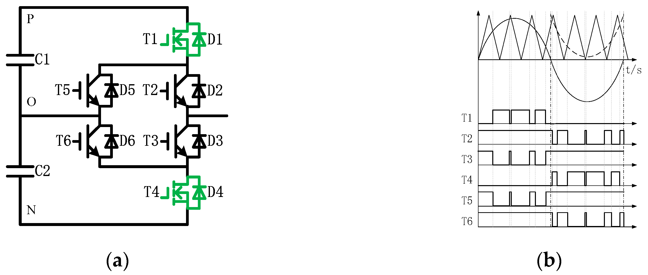
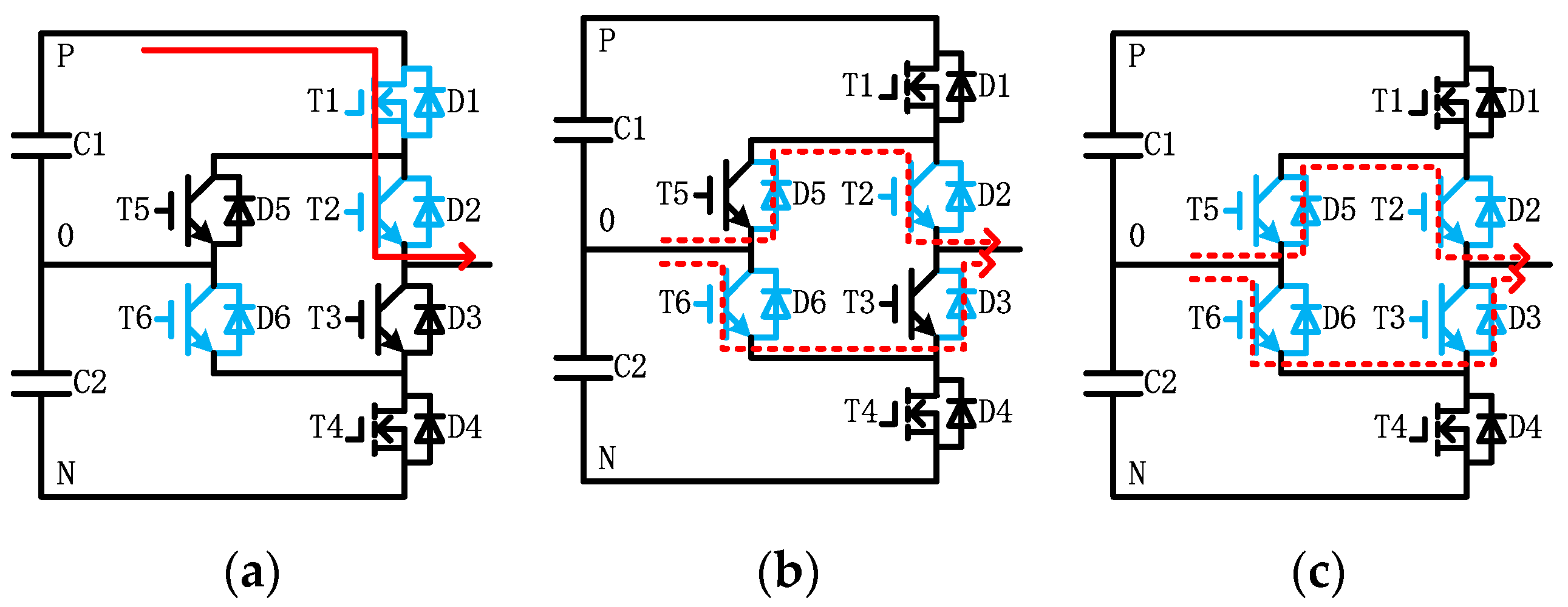
2. Proposed Hybrid Silicon Carbide (SiC) and Silicon (Si) ANPC Inverter

ANPC topology was developed on the basis of NPC topology. It replaces the two clamp diodes of the NPC topology with active switches. The proposed three-level hybrid ANPC inverter topology is shown in Figure 1a, in which T1 and T4 use SiC MOSFETs and the others use Si IGBTs. Other than the SiC and Si devices, the circuit configuration is exactly the same as a regular Si-based ANPC inverter.
In the proposed modulation, three switching status are designed as listed in Table 1. They can output three different voltage levels: P, O, N. In the P state, T1 and T2 are turned on, and the output voltage is Vdc/2. The O state is that the middle four tubes T2, T3, T5, and T6 are all turned on, and the voltage output is zero through two parallel circuits (T5/D5 and T2/D2, T6/D6 and T3/D3). In the N state, T3 and T4 are turned on, and the output voltage is −Vdc/2. The waveforms of the proposed modulation scheme are shown in Figure 1b. In the positive half cycle of the modulation wave, when the modulation wave is larger than the triangular carrier, T1 outputs a high level, while T3 and T5 output a low level. T2 and T6 are always high level during the positive half cycle of the modulation wave, and T4 is always low level. In the negative half cycle of the modulation wave, when the modulation wave is larger than the triangular carrier, T2 and T6 output high level, while T4 outputs low level. T3 and T5 are always high level during the negative half period of the modulation wave, and T1 is always low level.
In order to reduce the impact on the normal operation of the power grid, the power factor of photovoltaic inverters during operation must not be less than 0.95. Therefore, the theoretical analysis and comparison are performed under the unit power factor (which means the output voltage and current are in phase). The commutation process of P and O is shown in Figure 2. In the P state, T1, T2, and T6 are on, and current flows into the load through T1 and T2, and no current flows through T6. T1 is then turned off and the inverter enters the dead time. During the dead time, half of the current flows into the load through D3 and T6, and the other half flows into the load through D5 and T2. T3 and T5 are then zero voltage turned on, and the inverter enters the O state. In the O state, current flows into the load through two parallel circuits (D5 and T2, T6 and D3). The commutation process of N and O is shown in Figure 3. In the N state, T3, T4, and T5 are on, and current flows out of the load through T3 and T4, and no current flows through T5. T4 is then turned off and the inverter enters the dead time. During the dead time, half of the current flows into the load through T3 and D6, and the other half flows into the load through T5 and D2. T2 and T6 are then turned on at zero voltage, and the inverter enters the O state. In the O state, current flows into the load through two parallel circuits (T5 and D2, D6 and T3). It can be seen from the above analysis that although the driving signals of T1–T6 have high-frequency signals, after ignoring the zero-voltage soft switching losses, the hard switching losses are concentrated on T1 and T4. That is, in the proposed topology, the switching loss can be concentrated on the SiC MOSFETs by using this modulation strategy. In this modulation, the parallel loop in the O state can reduce the on-state loss compared to the commonly used single loop.

3. Loss Modeling

3.1. Device Loss Characteristics Comparison

The parameters of the single-phase independent inverter experimental platform are 1000 V DC side voltage and 3.3 kW rated power. Therefore, the device selection is 1200 V SiC MOSFET (C2M0080120D) and Si IGBT (FGH25T120SMD).

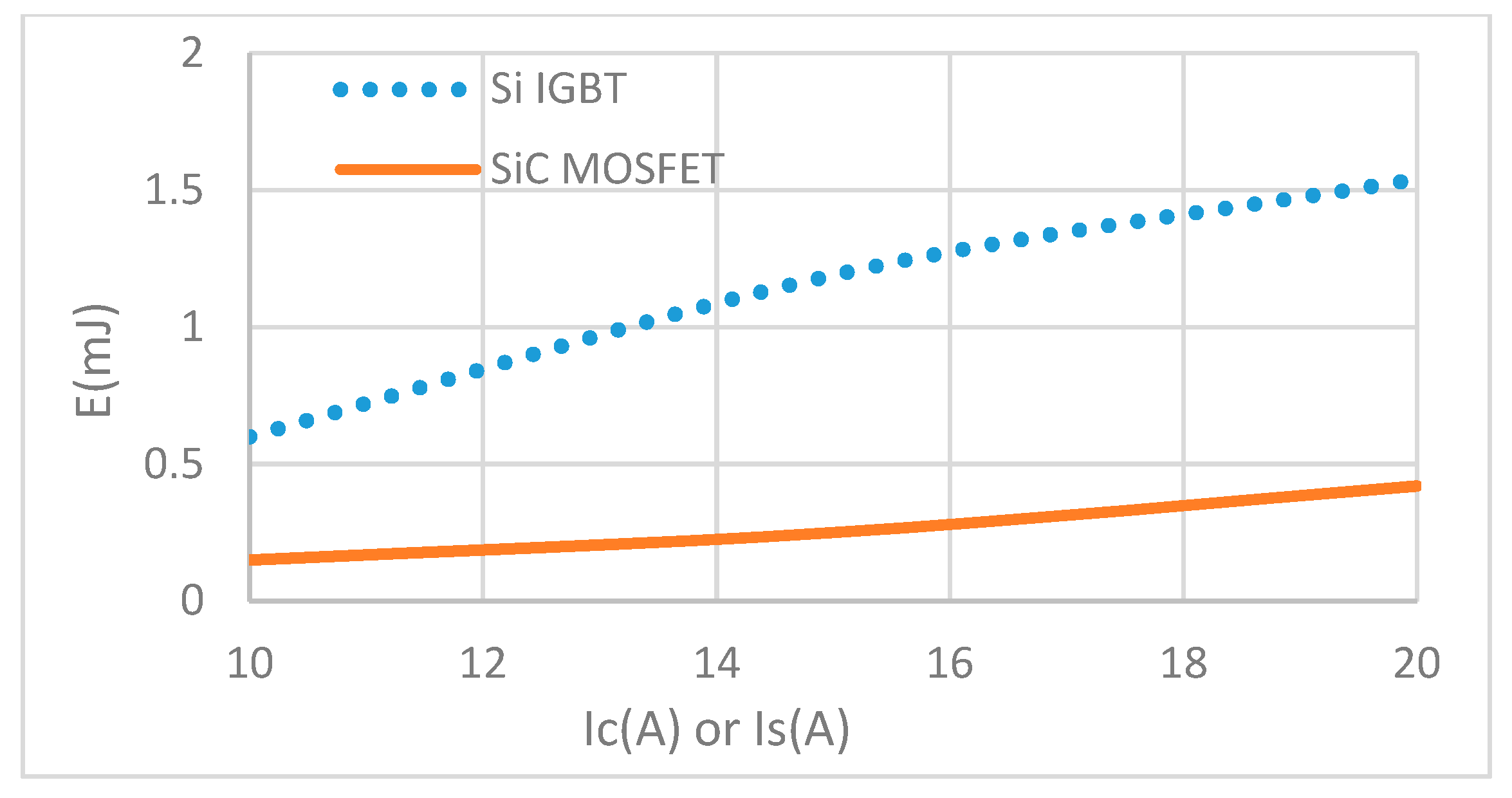
3.1.1. Power Device Switching Loss

As shown in Figure 4, the switching energy data is extracted from the device manuals of Si IGBT and SiC MOSFET. Because the switching loss modeling calculation is obtained by multiplying the single switching energy with the switching frequency, the single switching energy comparing results can reflect the comparison results of the switching loss. As shown in Figure 4, the switching loss of SiC MOSFET is much smaller than that of Si IGBT. Therefore, SiC MOSFETs have great advantages in high-frequency applications.

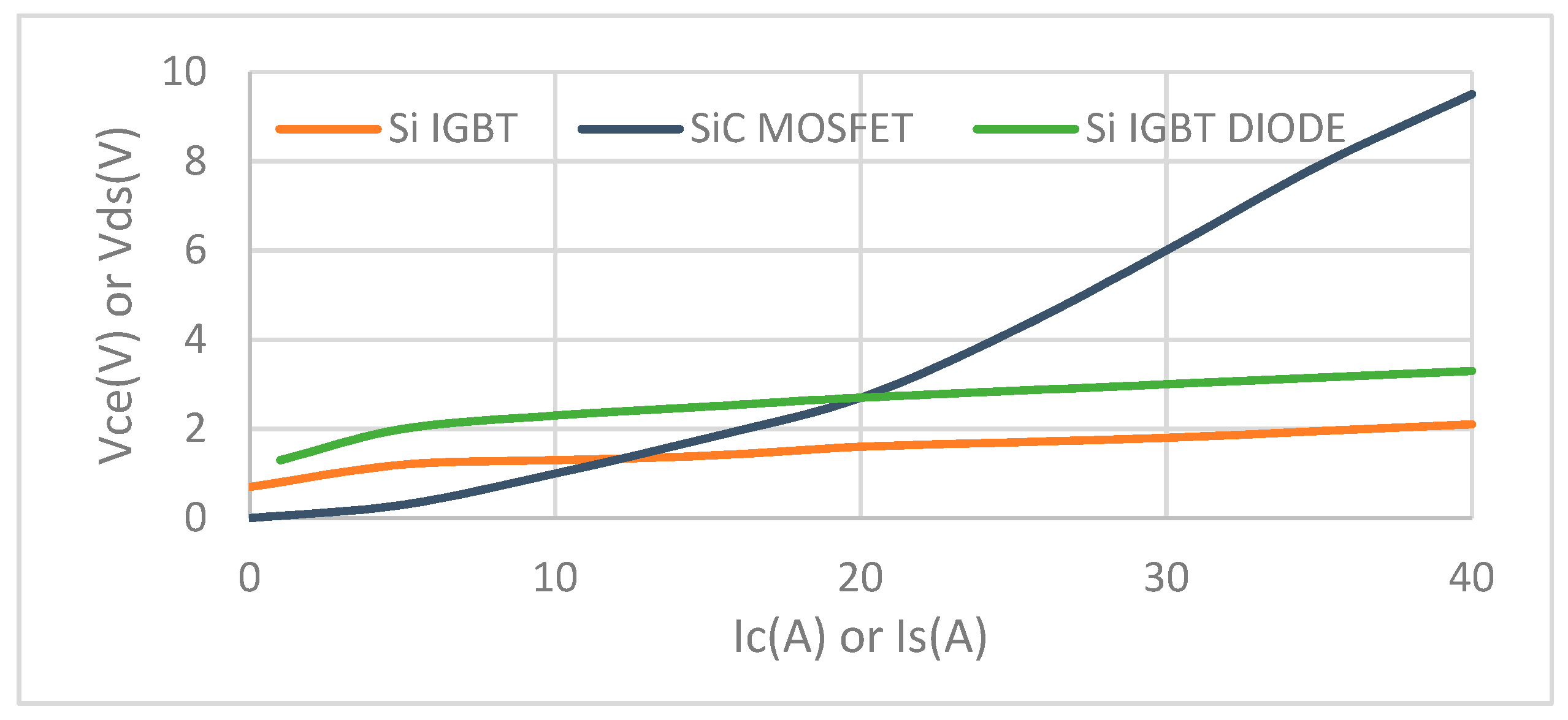
3.1.2. Power Device and Its Anti-Parallel Diode on-State Loss

Due to the synchronous rectification characteristics of the MOSFET, the on-state loss of its body diode is ignored. Therefore, this section does not compare the on-state characteristics of MOSFET body diodes. In Figure 5, the typical output characteristics of IGBT (25 °C VGE = 15 V) and its anti-parallel diode and MOSFET (25 °C VGE = 14 V) are proposed. The on-state loss of a power device was obtained by multiplying the current flowing through it and the voltage across the device when passing this current. Figure 5 shows the voltage change curves of Si IGBT, SiC MOSFET and the anti-parallel diode of Si IGBT when different currents flow. By comparing the voltages across power devices at a certain current, the magnitude relationship of the on-state loss can be obtained indirectly. As shown in Figure 5, it can be seen that when the current was below 20 A, the voltage across the SiC MOSFET was the smallest and the on-state loss was also the smallest. The voltage across the anti-parallel diode was the largest and the on-state loss was also the largest.

3.1.3. Reverse Recovery Loss of Anti-Parallel Diode

The reverse recovery loss of a diode is proportional to its reverse recovery charge (Qrr). Table 2 compares the reverse recovery charge of the anti-parallel diode of Si IGBT and the body diode of SiC MOSFET. It can be seen from Table 2 that the reverse recovery charge of the MOSFET body diode is low, indicating that its reverse recovery loss is lower. iF is the reverse current flowing through the diode. VR represents the reverse voltage applied across the diode.

3.2. Power Device Modeling

In order to theoretically compare the efficiency changes of each scheme, loss modeling is performed. According to the main parameter characteristics of the power devices at the typical junction temperature provided in the device manuals, loss models of the power devices can be established. According to the output characteristic curves of the power devices, i conduction loss models can be expressed as
P c o n = { P c o n , I G B T = I ( α ) V c e + I ( α ) 2 R c e P c o n , MOSFET = I ( α ) 2 R d s P c o n , DIODE = I ( α ) V f + I ( α ) 2 R f
where I ( α ) is the load current; V c e and V f are respectively represent the initial saturation voltage of the IGBT and the initial on-state voltage of the diode; R c e , R d s and R f are respectively represent the on-state resistance of the IGBT, the on-state resistance of the MOSFET and the on-state resistance of the diode of IGBT.
The switching losses of the IGBT and the MOSFET can be expressed as
P s w = { P s w , I G B T = E I G B T , s w ( I , T , U d c ) × f s P s w , M O S F E T = E MOSFET , s w ( I , T , U d c ) × f s
where E I G B T , s w ( I , T , U d c ) and E MOSFET , s w ( I , T , U d c ) respectively represent the energy values per unit switching cycle of IGBT and MOSFET as a function of current, temperature, and bus voltage.
The reverse recovery loss of a diode can be expressed as
P D , r e c = E D , r e c ( I , T , U d c ) × f s
where E D , r e c ( I , T , U d c ) represents the reverse recovery energy value per unit switching cycle of the diode as a function of current, temperature, and bus voltage.

3.3. Loss Modeling of the Proposed Scheme

Because the upper and lower arms of one phase ANPC topology are symmetrical, only the losses of the upper half arms (T1, T2, and T5) need to be analyzed. T1 is SiC MOSFET. In the positive half cycle of the modulation voltage, T1 is high-frequency switching. In the negative half cycle of the modulation voltage, T1 is turned off and no current flows. The conduction loss and switching loss of T1 are expressed as
P c o n , T 1 p w m N = 1 2 π 0 π P c o n , MOS × D ( α ) d α
P s w , T 1 p w m N = 1 2 π 0 π P s w , MOS d α
where D ( α ) is the duty cycle.
T2 is Si IGBT. During the positive half cycle of the modulation voltage, T2 is constantly on, and current always flows. During the negative half cycle of the modulation voltage, the load current flows through two parallel circuits during the OUL state and the dead time, so the current flowing through T2 during this time is half of the load current. In the negative half cycle, T2 is ZVS on, and the soft switching loss is ignored. The conduction loss and switching loss of T2 are expressed as
P c o n , T 2 p w m N = 1 2 π ( 0 π P c o n , IGBT × D ( α ) d α + 0 π P c o n , IGBT , OO × ( 1 D ( α ) ) d α )
P c o n , IGBT , OO = I ( α ) ( V c e + I ( α ) 2 R c e )
During the negative half cycle of the modulation voltage, in the OUL state and the dead time, half of the load current flows through D2. The conduction loss and reverse recovery loss of D2 are expressed as
P c o n , D 2 p w m N = 1 2 π π 2 π | P c o n , D I O D E , O O | × ( 1 | D ( α ) | ) d α
P c o n , D I O D E , O O = I ( α ) V f + I ( α ) 2 2 R f
P r e c , D 2 p w m N = 1 2 π π 2 π | P D , r e c , OO | d α
P D , r e c , OO = E D , r e c ( I 2 , T , U d c ) × f s
During the positive half cycle of the modulation voltage, T5 is ZVS on, and this soft switching loss is ignored. During the negative half cycle of the modulation voltage, T5 is always on. During OUL state and dead time, half of the load current flows through T5. The conduction loss of T5 can be expressed as
P c o n , T 5 p w m N = 1 2 π π 2 π | P c o n , IGBT , OO | × ( 1 | D ( α ) | ) d α
During the positive half cycle of the modulation voltage, in the O state and dead time, half of the load current flows through D5. The on-state loss and reverse recovery loss of D5 can be expressed as
P c o n , D 5 p w m N = 1 2 π 0 π P c o n , DIODE , OO × ( 1 D ( α ) ) d α
P r e c , D 5 p w m N = 1 2 π 0 π P D , r e c , OO d α

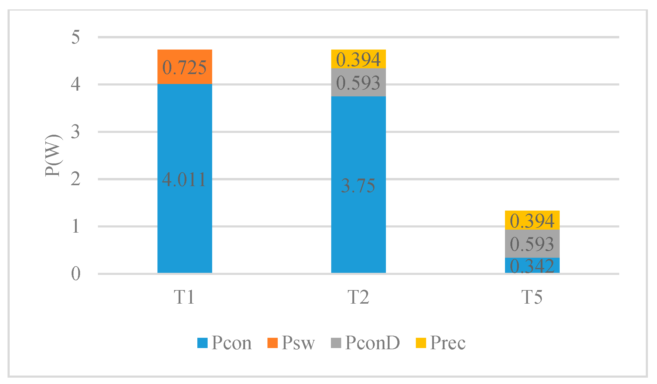
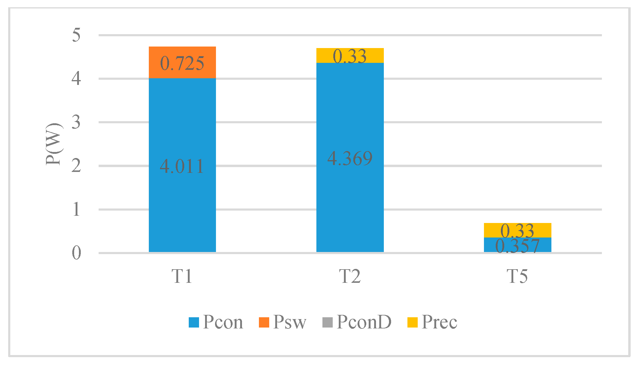
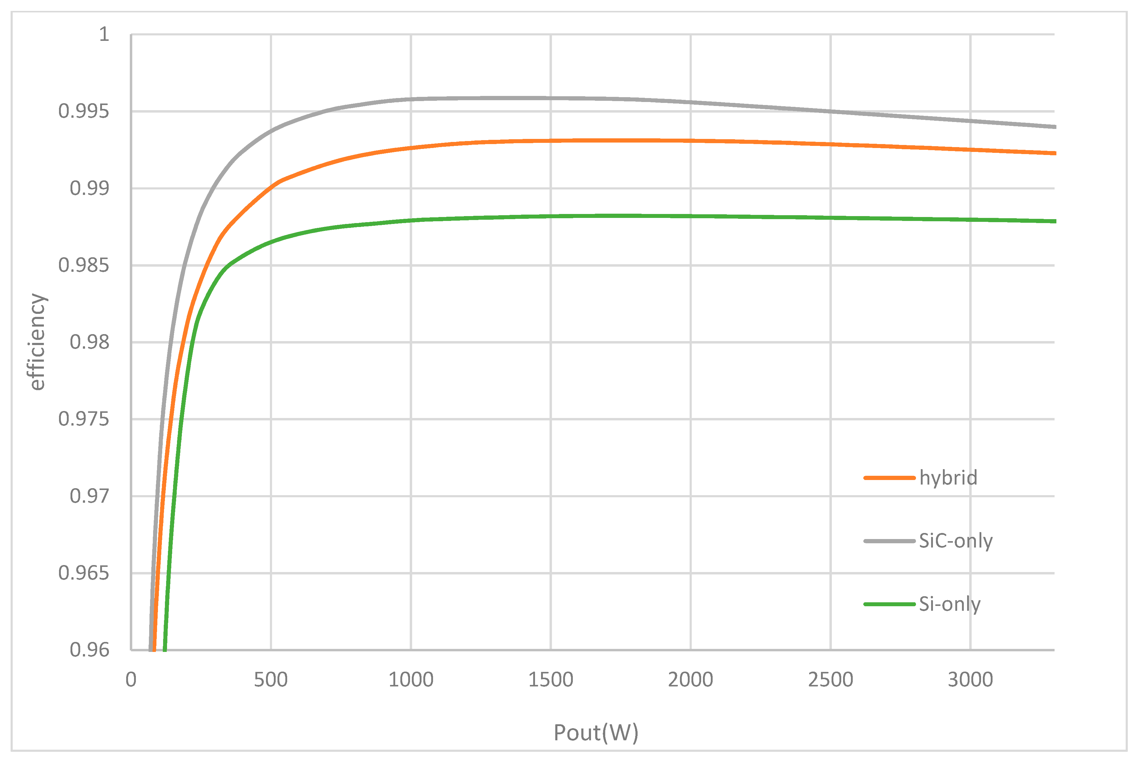
3.4. Comparison of Theoretical Analysis Results
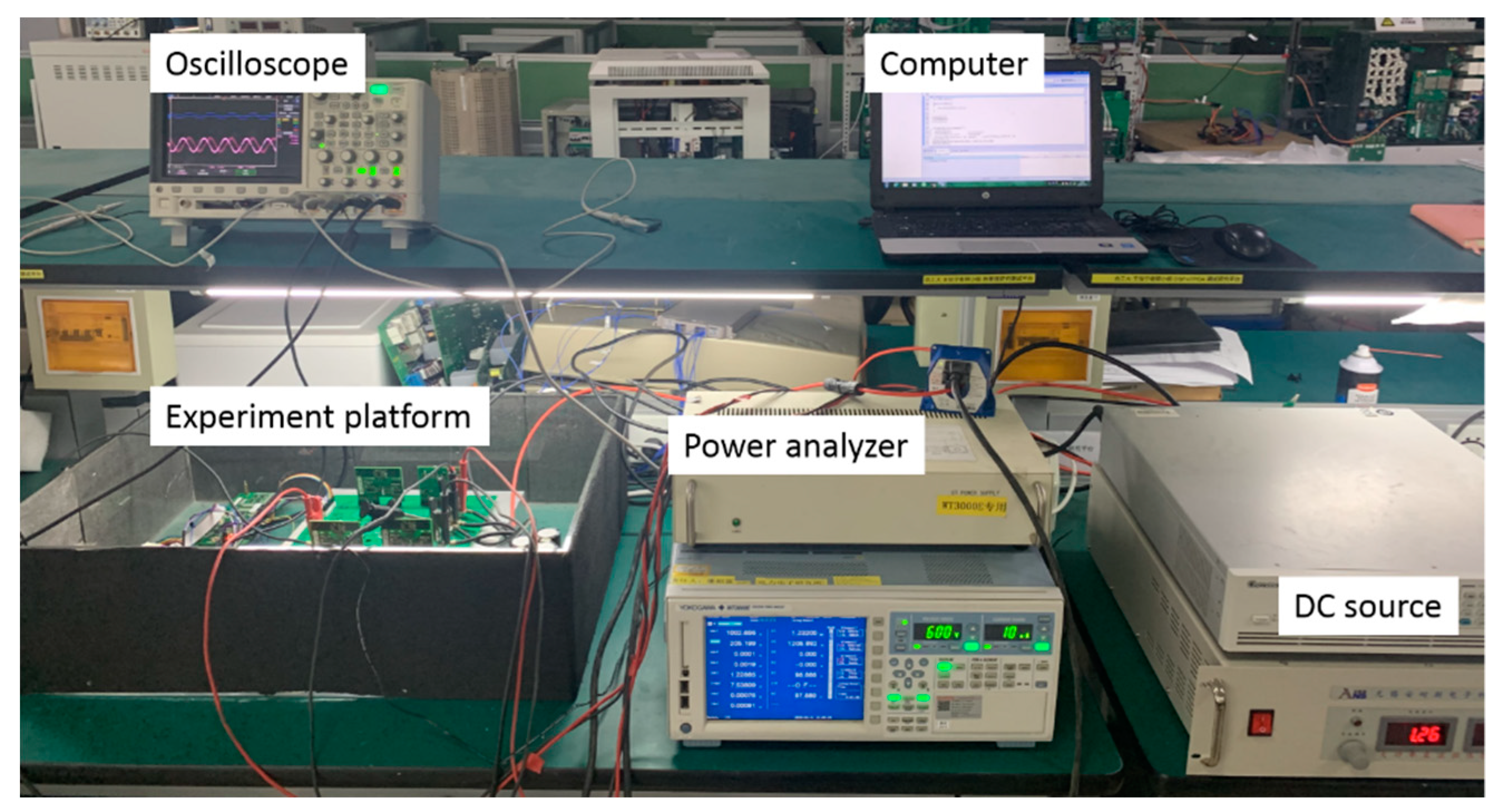
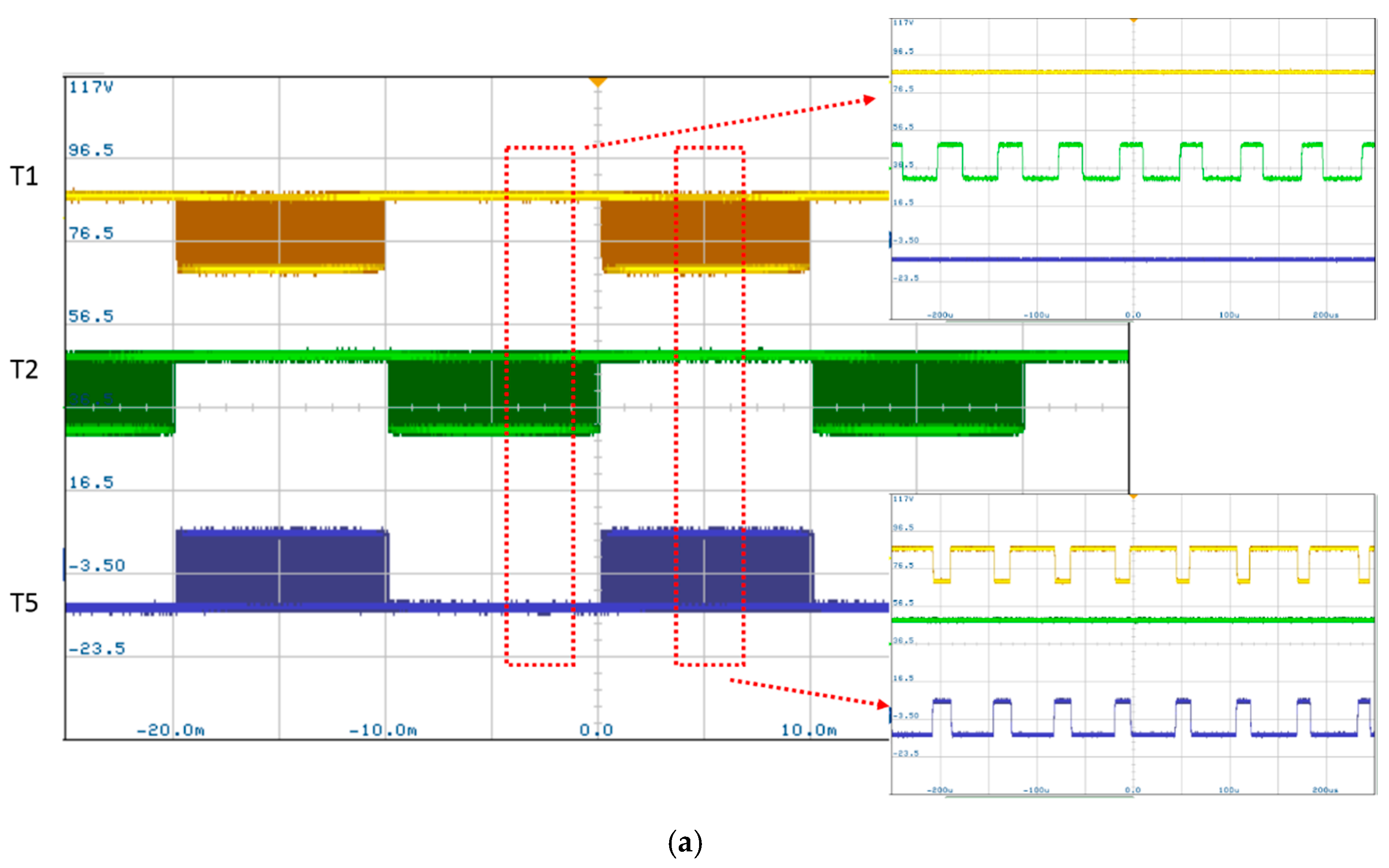
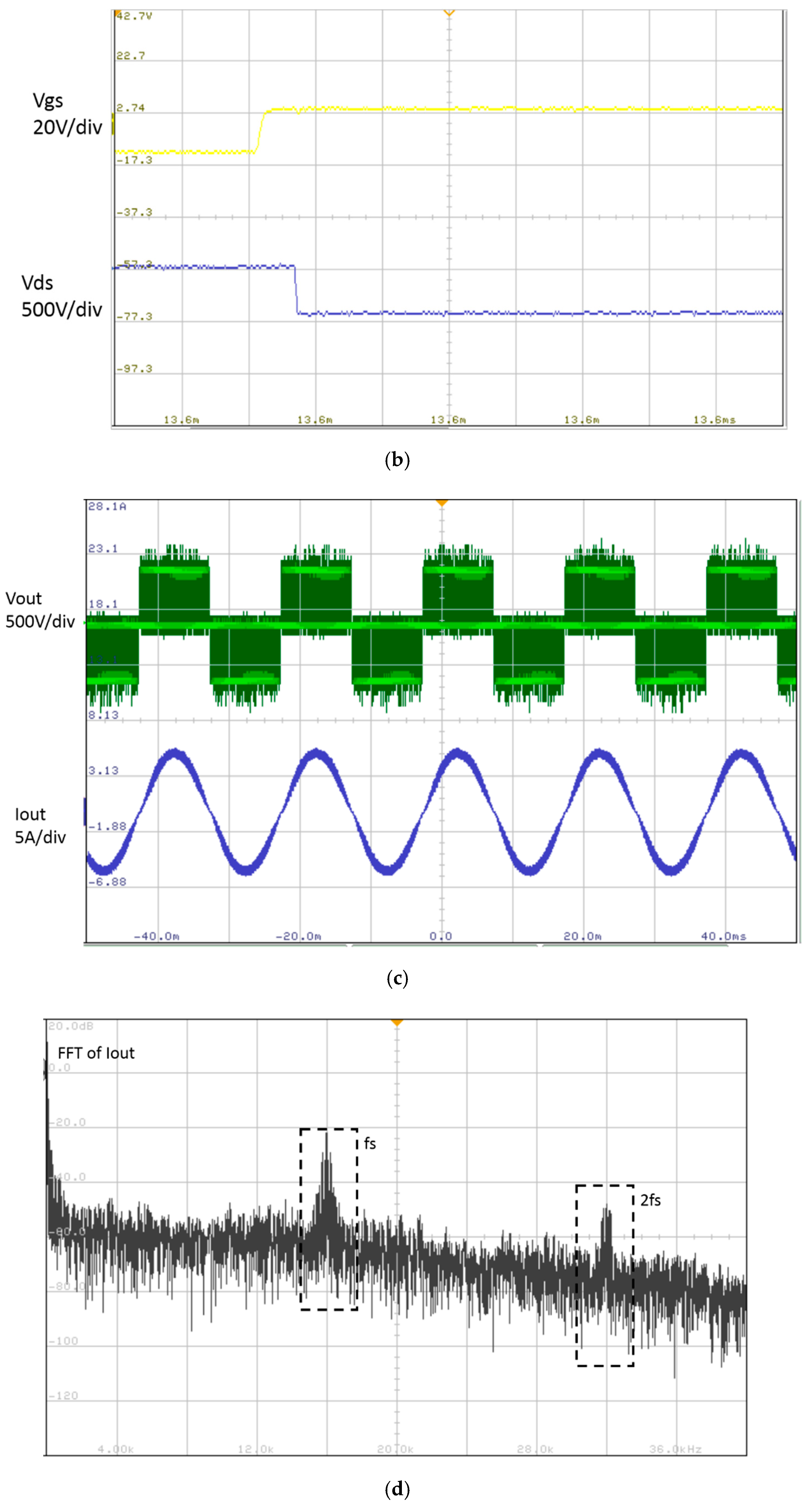
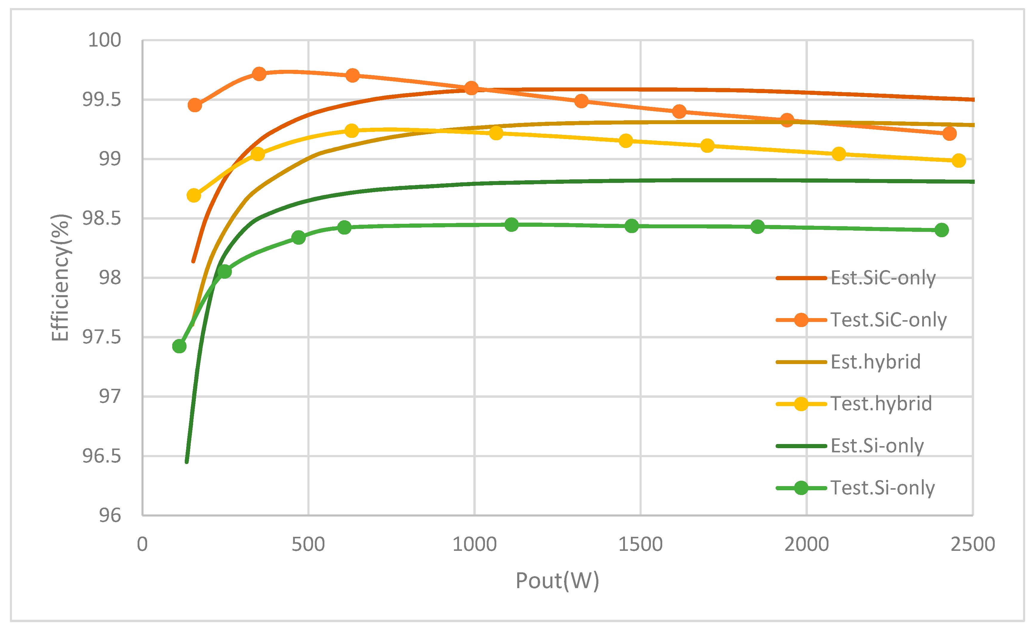
The inverter loss model is established in mathCAD according to the above formulas. The inverter operates at a unit power factor, while the bus voltage is 1000 V, the switching frequency is 16 kHz, and the rated power is 3.3 kW. With the data derived from datasheets and implementing the loss models, the loss distribution and efficiency of ANPC inverters with three configurations (hybrid SiC and Si, Si-only, and SiC-only) are estimated. All the calculations are applying the same proposed modulation strategy to make the results of comparison fair.
Since the one-phase circuit is symmetrical, half of the switches are considered. Figure 6 shows the loss distribution of the upper half bridge arms of the hybrid SiC and Si ANPC topology with the proposed modulation. It can be seen that the switching losses are all concentrated on T1 (SiC MOSFET), and the proportion is small. The main losses are the on-state losses of T1 and T2, followed by the on-state losses of D2 and D5. Figure 7 shows the loss distribution of the upper half-bridge arms of the Si-only ANPC topology with the same modulation. It can be seen that the switching loss of T1 accounts for a large proportion, and the value of other losses is not much different from that of the hybrid SiC and Si ANPC topology. Figure 8 shows the loss distribution of the upper half-bridge arms of the SiC-only ANPC topology under the same modulation. It can be seen that there is not much difference between the switching loss and the conduction loss compared to the hybrid SiC and Si ANPC topology. However, due to the synchronous rectification characteristics of the MOSFET, the reverse recovery loss of the diode in this scheme is small, so the total loss is reduced.
Figure 9 shows the efficiency curves of the hybrid SiC and Si, Si-only, and SiC-only schemes under the proposed modulation at different power levels with the rated power of 3.3 kW. Among the three topologies, the Si-only topology has the lowest efficiency curve, and its maximum efficiency is about 98.82%. The SiC-only topology has the highest efficiency curve, which is about 0.58–0.76% higher than the Si-only topology efficiency curve, and the maximum efficiency is about 99.58%. The efficiency of the hybrid SiC and Si topology is about 0.49% higher than that of the Si-only topology, about 0.17–0.27% lower than that of the SiC-only topology, and the maximum efficiency is about 99.31%. Therefore, this hybrid SiC and Si ANPC scheme using only two SiC MOSFETs is very cost-effective.

4. Experiment

The experiments were performed on single-phase independent ANPC inverter platforms. The main circuit were three different configurations of ANPC topologies: Si-only, SiC-only, and hybrid SiC and Si ANPC topologies. Except for the device configuration, the other configurations were identical. The efficiency curves of SiC and Si hybrid topology, Si-only topology and SiC-only topologies, were tested experimentally. The efficiency curves were measured by a power analyzer. The model of the power analyzer used was WT3000, and its test error was 0.02%. The selected Si IGBT and SiC MOSFET models were respectively FGH25T120SMD and C2M0080120D discrete devices in To247 packages. Considering that the Si IGBT cannot withstand very high switching frequency, the switching frequency is set to 16 kHz. The platform parameters are shown in Table 3. Photos of the experimental platform are shown in Figure 10.
Figure 11a shows the driving waveforms of the proposed modulation. The driving signal of T1 outputs high-frequency PWM wave in half of the power frequency period, and the other half period is constantly low; T2 outputs high-frequency PWM wave in half of the power frequency period, and the other half period is constant high level; T5 outputs a high-frequency PWM wave in half the power frequency period, and the other half period is constantly high. The driving waveforms of T1 and T5 are always complementary. Figure 11b is the waveforms of the drive voltage and the voltage across the device (T1 is taken as an example). When the driving voltage is high, the device is turned on, and the voltage across the device is 0. When the driving voltage is low, the device is turned off, and the voltage across the device is half the DC bus voltage. Figure 11c shows the output voltage and the current waveforms when the output current is 3 A. Figure 11d is the FFT (fast fourier transformation )of Iout.
The estimated efficiency curves and the tested efficiency curves of the proposed hybrid SiC and Si ANPC inverter, SiC-only ANPC inverter, and Si-only ANPC inverter are compared together in Figure 12. Consistent with the estimated efficiency curves, the Si-only topology has the lowest efficiency curve, and its maximum efficiency is about 98.45%. The SiC-only topology has the highest efficiency curve, which is about 0.76–1.27% higher than the Si-only topology efficiency curve, and the maximum efficiency is about 99.72%. The efficiency of the hybrid SiC and Si topology is about 0.58–0.90% higher than that of the Si-only topology, about 0.30–0.68% lower than that of the SiC-only topology, and the maximum efficiency is about 99.24%. Because the loss modeling only considered the power device part and did not consider the passive part loss, and the efficiency of the actual experimental test included the loss of the passive device, the experimental results were slightly lower than the theoretical analysis results. According to the official website of DigiKey Electronics, the hybrid scheme cost $63.72, while the all-SiC and all-Si separately cost $116.76 and $37.2. It can be seen that the hybrid scheme is a very cost-effective solution.

5. Conclusions

In this paper, a hybrid SiC and Si ANPC topology and a specific modulation were proposed. This proposed hybrid scheme has the following characteristics:
  • High-frequency switching losses were concentrated on SiC devices, so the switching losses were reduced;
  • In the 0 state of the ANPC three-level inverter, the current flowed through two parallel circuits, so the on-state loss was reduced;
  • The efficiency of the hybrid scheme was found to be around 0.58–0.90% higher than the traditional Si-only topology;
  • The efficiency of the hybrid scheme was found to be around 0.30–0.68% lower than the traditional SiC-only topology;
  • The cost of the proposed hybrid topology was about half that of the SiC-only topology.
The conclusion proved that the proposed hybrid topology was a cost-effective application structure. This topology can achieve high efficiency while controlling costs and was very suitable for engineering applications. In the future, we will continue to study other possible hybrid application schemes in ANPC topology and conduct comprehensive comparative studies.

Author Contributions

Conceptualization, Z.F., X.Z., and J.W.; Formal analysis, Z.F. and J.W.; Funding acquisition, X.Z.; Investigation, S.Y.; Software, Z.F. and S.Y.; Validation, Z.F.; Writing—original draft, Z.F.; Writing—review and editing, X.Z. All authors have read and agreed to the published version of the manuscript.

Funding

This work was funded by the Joint Funds of the National Natural Science Foundation of China (U1766207), The Natural Science Foundation of China (51677049).

Conflicts of Interest

The authors declare no conflict of interest.

References

  1. Chen, Q.; Wang, Q.; Li, G.; Ding, S. The Control of Unequal Power Losses Distribution in Three-Level Neutral-Point-Clamped VSC. In Proceedings of the 2012 15th International Conference on Electrical Machines and Systems (ICEMS), Sapporo, Japan, 21–24 October 2012. [Google Scholar]
  2. Bruckner, T.; Bemet, S. Loss Balancing in Three-Level Voltage Source Inverters applying Active NPC Switches. In Proceedings of the 2001 IEEE 32nd Annual Power Electronics Specialists Conference (IEEE Cat. No.01CH37230), Vancouver, BC, Canada, 17–21 June 2001. [Google Scholar]
  3. Chen, F.; Ding, X.; Lodhia, E. Efficiency and Current Harmonics Comparison Between SiC and Si Based Inverters for Microgrids. Energy Procedia 2016, 103, 298–303. [Google Scholar] [CrossRef]
  4. Ding, X.; Chen, F.; Du, M.; Guo, H.; Ren, S. Effects of silicon carbide MOSFETs on the efficiency and power quality of a microgrid-connected inverter. Appl. Energy 2017, 201, 270–283. [Google Scholar] [CrossRef]
  5. Gioia, A.D.; Brown, I.P. Silicon and hybrid Si-SiC tandem inverter analytical loss characterization and comparison to PWM-modulated voltage source inverter. In Proceedings of the IEEE Energy Conversion Congress and Exposition (ECCE), Montreal, QC, Canada, 20–24 September 2015. [Google Scholar]
  6. He, J.; Katebi, R.; Weise, N.; Demerdash, N.A.O.; Wei, L. A Fault-Tolerant T-Type Multilevel Inverter Topology With Increased Overload Capability and Soft-Switching Characteristics. IEEE Trans. Ind. Appl. 2017, 53, 2826–2839. [Google Scholar] [CrossRef]
  7. Anthon, A.; Zhang, Z.; Andersen, M.A.E.; Holmes, D.G. The Benefits of SiC MOSFETs in a T-Type Inverter for Grid-Tie Applications. IEEE Trans. Power Electron. 2017, 32, 2808–2821. [Google Scholar] [CrossRef] [Green Version]
  8. Zhang, D.; He, J.; Pan, D. A Megawatt-Scale Medium-Voltage High Efficiency High Power Density “SiC+Si” Hybrid Three-Level ANPC Inverter for Aircraft Hybrid-Electric Propulsion Systems. In Proceedings of the IEEE Energy Conversion Congress and Exposition (ECCE), Portland, OR, USA, 23–27 September 2018. [Google Scholar]
  9. He, J.; Zhang, D.; Pan, D. An Improved PWM Strategy for “SiC+Si” Three-Level Active Neutral Point Clamped Converter in High-Power High-Frequency Applications. In Proceedings of the IEEE Energy Conversion Congress and Exposition (ECCE), Portland, OR, USA, 23–27 September 2018. [Google Scholar]
  10. Pan, D.; Zhang, D.; Immer, C.; Dame, M.; He, J. Pump-Back Validation of A Medium Voltage High-Frequency “SiC+Si” Hybrid Three-Level ANPC Inverter for Hybrid-Electric Propulsion Application. In Proceedings of the 2019 IEEE International Electric Machines & Drives Conference (IEMDC), San Diego, CA, USA, 12–15 May 2019. [Google Scholar]
  11. Pan, D.; Zhang, D.; He, J.; Immer, C.; Dame, M. Control of MW-Scale High-Frequency “SiC+Si” Multilevel ANPC Inverter in Pump-Back Test for Aircraft Hybrid-Electric Propulsion Applications. IEEE J. Emerg. Sel. Top. Power Electron. 2020. (Early Access). [Google Scholar] [CrossRef]
  12. Zhang, L.; Liu, S.; Chen, G.; Yang, X. Evaluation of Hybrid Si/SiC Three-Level Active Neutral-Point-Clamped Inverters. In Proceedings of the 2019 IEEE 28th International Symposium on Industrial Electronics (ISIE), Vancouver, BC, Canada, 12–14 June 2019. [Google Scholar]
  13. Guan, Q.; Li, C.; Zhang, Y.; Wang, S.; Xu, D.D.; Li, W.; Ma, H. An Extremely High Efficient Three-Level Active Neutral-Point-Clamped Converter Comprising SiC and Si Hybrid Power Stages. IEEE Trans. Power Electron. 2018, 33, 8341–8352. [Google Scholar] [CrossRef]
  14. Sahan, B.; Mueller, C.R.; Lenze, A.; Czichon, J.; Slawinski, M. Combining the benefits of SiC T-MOSFET and Si IGBT in a novel ANPC power module for highly compact 1500-V grid-tied inverters. In Proceedings of the PCIM Europe 2019, Nuremberg, Germany, 7–9 May 2019. [Google Scholar]
  15. Lwon, B.H.; Bae, K.C.; Kim, S.M.; Lee, K.B. Detecting Method for an Open-Switch Fault of SiC MOSFET and Si IGBT in Hybrid ANPC Inverter System. In Proceedings of the 2019 IEEE Energy Conversion Congress and Exposition (ECCE), Baltimore, MD, USA, 29 September–3 October 2019. [Google Scholar]
  16. Li, C.; Lu, W.; Wang, Y. Space Vector Modulation for SiC & Si Hybrid Active Neutral Point Clamped Converter. In Proceedings of the IEEE International Power Electronics and Application Conference and Exposition (PEAC), Shenzhen, China, 4–7 November 2018. [Google Scholar]
  17. Li, C.; Lu, R.; Li, C.; Gu, X.; Fang, Y. Space Vector Modulation for SiC and Si Hybrid ANPC Converter in Medium-Voltage High-Speed Drive System. IEEE Trans. Power Electron. 2020, 35, 3390–3401. [Google Scholar] [CrossRef]
  18. Feng, Z.; Zhang, X.; Yu, S.; Wang, J. Loss Analysis and Measurement of ANPC Inverter Based on SiC & Si Hybrid Module. In Proceedings of the IEEE International Power Electronics and Application Conference and Exposition (PEAC), Shenzhen, China, 4–7 November 2018. [Google Scholar]
  19. Zhang, L.; Lou, X.; Li, C.; Wu, F.; Gu, Y. Evaluation of Different Si/SiC Hyrbid Three-Level Active NPC Inverters for High Power Density. IEEE Trans. Power Electron. 2019. (Early Access). [Google Scholar] [CrossRef]
Figure 1. Proposed topology and modulation strategy waveform: (a) Proposed hybrid ANPC topology; (b) Proposed modulation strategy waveform.
Energies 13 01159 g001
Figure 2. Commutation process between P and O: (a) P; (b) dead time; (c) O.
Energies 13 01159 g002
Figure 3. Commutation process between N and O: (a) N; (b) dead time; (c) O.
Energies 13 01159 g003
Figure 4. Switching energy curves of silicon (Si) IGBT and silicon carbide (SiC) MOSFET at 25 °C.
Energies 13 01159 g004
Figure 5. Typical output characteristics of Si IGBT and its anti-parallel diode and SiC MOSFET.
Energies 13 01159 g005
Figure 6. Loss distribution of T1, T2, and T5 in hybrid SiC and Si topology.
Energies 13 01159 g006
Figure 7. Loss distribution of T1, T2, and T5 in Si-only topology.
Energies 13 01159 g007
Figure 8. Loss distribution of T1, T2, and T5 in SiC-only topology.
Energies 13 01159 g008
Figure 9. Comparison of the efficiency of the hybrid, Si-only, and SiC-only schemes.
Energies 13 01159 g009
Figure 10. Photograph of the experimental platform.
Energies 13 01159 g010
Figure 11. Experiment waveforms (a) Driving waveforms of the proposed modulation; (b) Driving voltage and voltage across the device; (c) Output voltage and current waveform at 3 A output current; (d) FFT of Iout.
Energies 13 01159 g011aEnergies 13 01159 g011b
Figure 12. Comparison of prediction and experimental efficiency curves.
Energies 13 01159 g012
Table 1. Switching status of the proposed ANPC topology.
Output StatusT1T2T3T4T5T6Output Voltage
P110000/1+Vdc/2
O0110110
N00110/10−Vdc/2
Table 2. Diode reverse recovery loss comparison.
QrrTest Condition
IGBT anti-parallel diode197 nC25 °C, VR = 600 V, iF = 25 A, diF/dt = 200 A/µs
MOSFET anti-parallel diode165 nC25 °C, VR = 800 V, iF = 20 A, diF/dt = 350 A/µs
Table 3. Experiment platform parameters.
Rated Power Pe3.3 KW
Bus voltage Udc1000 V
Operating frequency fs16 kHz
Load Resistance R40 Ω
Filter inductor L0.9 mH
Filter capacitor C200 uF
DC side capacitor Cdc4700 uF*2

