Article

Fabrication and Characterization of Cu2ZnSnSe4 Thin-Film Solar Cells using a Single-Stage Co-Evaporation Method: Effects of Film Growth Temperatures on Device Performances

1
Photovoltaics Laboratory, Korea Institute of Energy Research (KIER), 152-Gajeong-ro, Yuseong-gu, Daejeon 34129, Korea
2
Department of Renewable Energy Engineering, Faculty of Environmental Technology, University of Science and Technology (UST), 217-Gajeong-ro, Yuseong-gu, Daejeon 34113, Korea
3
Department of Material Science and Engineering, Korea Advanced Institute of Science and Technology (KAIST), 291, Daehak-ro, Yuseong-gu, Daejeon 34141, Korea
*
Authors to whom correspondence should be addressed.
Energies 2020, 13(6), 1316; https://doi.org/10.3390/en13061316
Submission received: 31 January 2020 / Revised: 24 February 2020 / Accepted: 6 March 2020 / Published: 12 March 2020

Abstract

:
Kesterite-structured Cu2ZnSnSe4 (CZTSe) is considered as one of the Earth-abundant and non-toxic photovoltaic materials. CZTSe films have been prepared using a single-step co-evaporation method at a relatively low temperature (i.e., below 500 °C). Due to the volatile nature of tin-selenide, the control over substrate temperature (i.e., growth temperature) is very important in terms of the deposition of high-quality CZTSe films. In this regard, the effects of growth temperatures on the CZTSe film morphology were investigated. The suitable temperature range to deposit CZTSe films with Cu-poor and Zn-rich compositions was 380–480 °C. As the temperature increased, the surface roughness of the CZTSe film decreased, which could improve p/n junction properties and associated device performances. Particularly, according to capacitance-voltage (C-V) and derived-level capacitance profiling (DLCP) measurements, the density of interfacial defects of CZTSe film grown at 480 °C showed the lowest value, of the order of ~3 × 1015 cm−3. Regardless of applied growth temperatures, the formation of a MoSe2 layer was rarely observed, since the growth temperature was not high enough to have a reaction between Mo back contact layers and CZTSe absorber layers. As a result, the photovoltaic (PV) device with CZTSe film grown at 480 °C yielded the best power conversion efficiency of 6.47%. It is evident that the control over film growth temperature is a critical factor for obtaining high-quality CZTSe film prepared by one-step process.

Graphical Abstract

1. Introduction

Climate changes induced by increased emission of greenhouse gases have become a global issue in the past decades. Currently, solar energy is recognized as one of the most promising options to address the issue [1,2]. Various photovoltaic (PV) solar cell technologies are currently being developed in three formats: (1) crystalline silicon (c-Si)-based, (2) thin film-based, and (3) emerging material-based technologies [3,4]. Even though the global PV market share of thin-film PV modules based on CdTe, Cu(In,Ga)Se2 (CIGS), and a-Si solar cells is currently only less than 5%, while the c-Si-based market far exceeds a 90% share of the market [5], it is obvious that the market will noticeably grow according to technology and industry trends in the near future. It is worth noting here that the CIGS solar cell is the only technology that has recently increased its market share among the aforementioned thin film technologies [5,6]. If Earth-abundant materials can be successfully applied into the absorber layer, replacing In and Ga elements in a CIGS system for a stable and high-efficiency solar cell, it will be even more meaningful for fabrication cost reduction and PV deployment expansion [7]. The Cu2ZnSn(S,Se)4 (CZTSSe) compound family is a potential source of materials among numerous Earth-abundant element-based compounds that have been intensively explored for PV application [8,9,10]. Since the IBM research group opened up a novel deposition method (i.e., hydrazine-based solution process), a power conversion efficiency (PCE) record of 12.6% has been attained for a CZTSSe device [11]. However, there has been no further improvement in the device’s efficiency, and so far it has been hard to scale up the device size, even if the solution process is cost effective. In terms of uniform and large-area CZTSSe film deposition, the vacuum-based processes are more suitable as a scalable method. In this respect, DGIST has reported 11.3% PCE using sputter-deposition of a precursor followed by post-annealing (denoted as a two-step process) [12]. National renewable energy laboratory (NREL) has achieved the PCE of 9.15% for a Cu2ZnSnSe4 (CZTSe)-based PV device using a co-evaporation method (denoted as a one-step process) [13]. Given that, among currently available processes, a one-step process is the simplest way to produce CZTSSe absorbers, it may be considered as a feasible method for commercializing CZTSSe solar cells. Nevertheless, details on the growth of co-evaporated CZTSSe films and the optimization of devices have not been studied systemically. Presumably, the difficulty in obtaining high-quality CZTSSe films could be associated with the volatile nature of Sn-Se compounds and the narrow phase stability zone of the CZTSSe material system [14,15,16].
In this work, the effects of growth temperature on the morphological, structural, and electrical properties of CZTSe films prepared by a single-step co-evaporation method were investigated. The desirable temperature range to deposit high-quality CZTSe films with Cu-poor and Zn-rich compositions was found. At the optimal temperature (480 °C), the surface roughness of CZTSe films was decreased, leading to a reduction in the densities of bulk and interfacial defects. According to derived-level capacitance profiling (DLCP) measurement, the estimated carrier density of the CZTSe film is in the range of ~1 × 1016 cm−3. As a result, the best CZTSe-based solar cell yielded the PCE of 6.47%. This suggests that the control over film growth temperature is an important factor for obtaining a high-quality CZTSe film prepared by the single-step process.

2. Experimental Details

The back electrode was prepared by depositing the molybdenum (Mo) on the 5 × 5 cm2 soda-lime glass (SLG) with a 700 nm thickness using a direct-current magnetron spurting. A bilayer approach for the deposition of Mo on soda-lime glass (SLG) was adopted with a 280-nm-thick bottom layer at a high processing pressure for better adhesion and a 420-nm-thick top layer at a low pressure for a low resistivity.
The growth of CZTSe absorber films on Mo/SLG substrates was carried out by single-stage co-evaporation technique. CZTSe films were prepared on Mo-coated SLG substrates in a manner previously described [17]. Note that the co-evaporator was also used to deposit a pure sulfur CZTS film. CZTSe films were deposited at various growth temperatures by using four effusion cells for Cu, Zn, Sn, and Se elements. The growth temperature during film deposition was adjusted from 380 to 480 °C. A film with approximately 1 µm thickness was produced by a 90-min deposition process. When the substrate temperature was cooled down naturally, Zn, Sn, and Se elements were additionally supplied while the shutter of the Cu source was closed. The purpose of adopting the abovementioned conditions is to suppress Se vacancies in the film as well as the decomposition of the CZTSe film at relatively high temperature [18,19]. The entire temperature profile for the CZTSe film deposition is given as shown in Figure 1.
The typical device structure for high-efficiency CIGS and CZTSSe PVs was employed throughout the studies [17,20]. A 60-nm-thick CdS buffer layer (n-type) was deposited on the CZTSe/Mo/SLG by using chemical bath deposition (CBD). The thickness of the CdS buffer layer was monitored via quartz crystal microbalance (QCM). For the window layer, an intrinsic zinc oxide with a 50 nm thickness and Al-doped zinc oxide with a 350 nm thickness were deposited by using a radio-frequency magnetron spurting on the CdS/CZTSe/Mo/SLG. Finally, the Al front grid was prepared by a thermal evaporator. The device area was 0.44 cm2.
The structural characterizations for CZTSe films were performed using an X-ray diffractometer (Rigaku D/Max-2500, Japan) and Raman spectroscopy (N8 NEOS SENTERRA, USA). To verify the film microstructure, scanning electron microscope (SEM) images were taken using a Hitachi S-4700 filed-emission SEM, Japan. Energy-dispersive X-ray spectroscopy (EDS) connected to SEM equipment was used at an accelerating voltage of 20 KeV to estimate the chemical composition of CZTSe films. Current-voltage measurements were carried out using a McScience K201-LAB 50, South Korea under AM 1.5G illumination with an intensity of 100 mW/cm2. The spectral responses were measured using a McScience K3100, South Korea. A calibrated Si solar cell was used as a reference for the device measurement. To estimate the carrier density of CZTSe film, both capacitance-voltage (C-V) and derived-level capacitance profiling (DLCP) were performed using a precision LCR meter (Agilent 4284A, USA) at 300 K.

3. Results and Discussion

The CZTSe films were grown at various temperatures ranging from 350 to 530 °C to determine a suitable growth temperature range for high-quality CZTSe films. As seen in Figure 2a,b, when the growth temperature was set to 530 °C, a continuous film was not formed. The CZTSe films grown below 480 °C showed compact and continuous morphologies, even if few voids were formed. Actually, there was no significant change in the grain sizes. However, as seen in Figure 2i,j, when the growth temperature was less than 350 °C, the ratio of (Zn)/(Sn) concentrations was more than 2 and that of (Cu)/((Zn)+(Sn)) was lower than 0.6, which are values outside of the optimal composition ranges (e.g., for the CZTSSe-based record device, (Cu)/((Zn)+(Sn))~0.8 and (Zn)/(Sn)~1.1 [11]. Given that high-quality films possess compact and large-grained morphologies with suitable Cu-poor and Zn-rich compositions, the required growth temperatures to enable device-quality CZTSe films prepared by one-step method seem to be in the temperature range of 380~480 °C, as depicted in Figure 2c,h. The poor film coverage with island grains and unfavorable chemical composition could be associated with the high volatility of Sn-Se compounds during CZTSe film deposition [21,22]. Moreover, it was observed that as the growth temperature was increased from 380 to 480 °C, the surface roughness of the CZTSe films was reduced. The smoother surface could lead to an improvement in p/n junction properties and associated device performance.
To investigate the formation of secondary phases and the single-phase nature of CZTSe films, X-ray diffraction patterns of CZTSe films grown at various growth temperatures were measured, as shown in Figure 3. Regardless of various applied growth temperatures, all XRD peaks were assigned to the phase of CZTSe material (JCPDS No. 52-0868) and the films were observed to have (112)-preferred-orientation. This indicates that no secondary phases in the CZTSe films were observed. Nevertheless, the presence of secondary phases, such as ZnSe and Cu2SnSe3, in the films cannot be ruled out [23,24,25,26]. As seen in Figure 3b, the (112) peak was shifted toward a higher XRD diffraction angle when the film was deposited at the higher growth temperature. Such a peak shift seems to be related to the incorporation of sulfur residue from the co-evaporation chamber, since the co-evaporator was used to deposit pure CZTS sulfide and the vaporizing temperature of sulfur is very low.
To identify the formation of the secondary phases and impacts of various growth temperatures on CZTSe film, Raman scattering measurement was performed at room temperature with a 532 nm laser excitation. In literature, the A1 mode Raman peak of CZTSe and CZTS is located at 194–197 cm−1 and 322-327 cm−1, respectively [27,28,29,30,31,32]. Thus, as seen in Figure 4, the primary main peak of the films is assigned to the Al peak for CZTSe and the second main peak seems to be assigned to the A1 peak for CZTS. Furthermore, the Al peak for CZTSe films is shifted as a function of growth temperature and the intensity of peak at ~324 cm−1 is increased without a peak shift. This observation is consistent with the XRD result, as seen in Figure 3b. In general, high growth temperature could induce a small amount of sulfur incorporation if a small amount of sulfur exists in the chamber. Actually, the incorporation of sulfur can influence the bandgap of CZTSe films and voltage output of PV devices.
To evaluate the PV device performance with CZTSe films grown at various temperatures, the CZTSe film is incorporated as an absorber in the conventional structure for CIGS solar cells, for instance, ITO/i-ZnO window/CdS buffer/absorber/Mo back contact. The current density-voltage (J-V) characteristics of PV devices with a CZTSe film grown at various growth temperatures are shown in Figure 5a. In addition, the photovoltaic parameters measured from the J-V curves are listed in Table. 1. Basically, all PV parameters and device efficiencies improved gradually with an increase in the growth temperature for CZTSe film. The device efficiency prepared at the higher growth temperature of 480 °C increased from 1.36% to 6.08% because of the improvement in both shunt resistance and saturated recombination current density (J0), resulting in reduced VOC deficit (Table 1). Such improvements seem to be associated with the formation of a sturdy p/n junction by the reduction in the film surface roughness, as seen in Figure 2. In addition, the incorporated sulfur can affect device performance, since the cutoff of EQE spectra in the long-wavelength (Figure 5b) is decreased as a function of growth temperature. However, the current best cell is still lower than the highest value of 9.15% for a CZTSe film prepared by one-step method [13].
To understand defect properties of CZTSe PV devices, CV and DLCP measurements were performed. By fitting the CV and DLCP data (Figure S2a,c), various information such as free carriers, interface, and bulk defect densities were estimated and summarized, as seen in Table 2. They indicate that the density of interfacial defect was decreased, showing less than <1016 cm3 as the growth temperature increased, while the density of bulk defects for all PV devices remained at a similar level. Additionally, the depletion width of the CZTSe film grown at 480 °C was relatively larger than one of films grown at the lower temperatures. Consequently, this means that interface recombination was more dominant compared to bulk recombination and may be related to surface roughness.
Figure 6 shows that when MgF2 anti-reflection coating with a 100 nm thickness was applied, the device efficiency was slightly increased from 6.04% to 6.47% due to an increase in the spectral response at long wavelength, as shown in Figure 6b. Further studies may be needed to gain deeper insights into defect passivation by post-deposition treatment of alkali elements (e.g., Na, K, Rb, and Cs) [33,34,35]. Additionally, in order to increase the spectral response at the short wavelength region, a Zn(O,S) buffer layer can be considered as a wide bandgap and Cd-free material [36,37,38].

4. Conclusions

Earth-abundant Cu2ZnSnSe4 films were deposited on Mo-coated SLG substrates by using a single-stage co-evaporation method. The films were grown at various growth temperatures to determine a suitable growth temperature range for high-quality CZTSe films. When the films were grown at 380~480 °C, XRD and Raman data indicate that all films adopted a kesterite structure with I-4 space group without observation of secondary phase formation. Most of all, the surface roughness of the CZTSe film grown at the higher temperature of 480 °C was significantly decreased. As a result, the PV device efficiency was increased up to 6.47%, since both shunt resistance and saturated recombination current density were improved, leading to a reduction in the Voc deficit. According to C-V and DLCP measurements, the increase in the open circuit voltage of the device is consistent with a reduction in the density of interfacial defects. Overall, our results suggest that control over film growth temperature is a critical factor for obtaining high-quality CZTSe film prepared by one-step process. Moreover, alkali post-deposition treatment may enable improved device efficiency through defect passivation. By using a wider bandgap buffer layer (e.g., Zn(O,S)), spectral responses in the short wavelength region could be enhanced. Overall, such technologies may offer a pathway to higher device efficiency.

Supplementary Materials

Supplementary materials to this article can be found online at: https://www.mdpi.com/1996-1073/13/6/1316/s1.

Author Contributions

Conceptualization, D.S. and J.G.; methodology, D.S.; software, K.K.; validation, S.A. and D.S.; formal analysis, K.K. and Y.C.; investigation, M.R., Y.C. and D.S.; resources, A.C. and J.-S.C.; data curation, M.R. and H.J.; writing—original draft preparation, M.R.; writing—review and editing, D.S. and J.G.; visualization, M.R.; supervision, D.S., J.H.Y., and J.G.; project administration,. A.C.; funding acquisition, J.G. and J.H.Y. All authors have read and agreed to the published version of the manuscript.

Funding

This work was supported by the Korea Institute of Energy Technology Evaluation and Planning (KETEP), granted financial resources from the Ministry of Trade, Industry and Energy (MOTIE) of the Republic of Korea (No. 20173010012980). This research was also financially supported by the Framework of the Research and Development Program of the Korea Institute of Energy Research (KIER) (grant no. C0-2401-01) and the Technology Development Program to Solve Climate Changes of the National Research Foundation (grant no. 2016M1A2A2936753) funded by the Ministry of Science and ICT.

Conflicts of Interest

The authors declare no conflict of interest.

References

  1. Bakhiyi, B.; Labrèche, F.; Zayed, J. The photovoltaic industry on the path to a sustainable future—Environmental and occupational health issues. Environ. Int. 2014, 73, 224–234. [Google Scholar] [CrossRef] [PubMed]
  2. Jain, P. Greenhouse effect and climate change: Scientific basis and overview. Renew. Energy 1993, 3, 403–420. [Google Scholar] [CrossRef]
  3. Kibria, M.T.; Ahammed, A.; Sony, S.M.; Hossain, F.; Islam, S. A Review: Comparative studies on different generation solar cells technology. In Proceedings of the 5th International Conference on Environmental Aspects of Bangladesh, Dhaka, Bangladesh, 5–6 September 2014; pp. 51–53. [Google Scholar]
  4. Ranabhat, K.; Patrikeev, L.; Antal’evna-Revina, A.; Andrianov, K.; Lapshinsky, V.; Sofronova, E. An introduction to solar cell technology. J. Appl. Eng. Sci. 2016, 14, 481–491. [Google Scholar] [CrossRef] [Green Version]
  5. Philips, D.; Warmuth, W. Photovoltaics Report; Fraunhofer Institute for Solar Energy System: Freiburg, Germany, 2019; pp. 1–43. [Google Scholar]
  6. Płaczek-Popko, E. Top PV market solar cells 2016. Opto-Electron. Rev. 2017, 25, 55–64. [Google Scholar]
  7. Shin, S.W.; Han, J.H.; Park, C.Y.; Moholkar, A.V.; Lee, J.Y.; Kim, J.H. Quaternary Cu2ZnSnS4 nanocrystals: Facile and low cost synthesis by microwave-assisted solution method. J. Alloy. Compd. 2012, 516, 96–101. [Google Scholar] [CrossRef]
  8. Reddy, V.R.M.; Gedi, S.; Pejjai, B.; Park, C. Perspectives on SnSe-based thin film solar cells: A comprehensive review. J. Mater. Sci. Mater. Electron. 2016, 27, 5491–5508. [Google Scholar] [CrossRef]
  9. Siebentritt, S.; Schorr, S. Kesterites—A challenging material for solar cells. Prog. Photovolt. Res. Appl. 2012, 20, 512–519. [Google Scholar] [CrossRef]
  10. Li, W.; Li, Z.; Feng, Y.; Chen, M.; Li, W.; Zhong, G.-H.; Lu, Y.; Yang, C. Preparation of Cu2ZnSn(SxSe1−x)4 solar cells with two step sulfurization. Sol. Energy 2020, 197, 73–77. [Google Scholar] [CrossRef]
  11. Wang, W.; Winkler, M.T.; Gunawan, O.; Gokmen, T.; Todorov, T.K.; Zhu, Y.; Mitzi, D.B. Device characteristics of CZTSSe thin-film solar cells with 12.6% efficiency. Adv. Energy Mater. 2014, 4, 1301465. [Google Scholar] [CrossRef]
  12. Green, M.A.; Dunlop, E.D.; Levi, D.H.; Hohl-Ebinger, J.; Yoshita, M.; Ho-Baillie, A.W. Solar cell efficiency tables (version 54). Prog. Photovolt. Res. Appl. 2019, 27, 565–575. [Google Scholar] [CrossRef]
  13. Repins, I.; Beall, C.; Vora, N.; DeHart, C.; Kuciauskas, D.; Dippo, P.; To, B.; Mann, J.; Hsu, W.-C.; Goodrich, A. Co-evaporated Cu2ZnSnSe4 films and devices. Sol. Energy Mater. Sol. Cells 2012, 101, 154–159. [Google Scholar] [CrossRef]
  14. Wang, W.; Chen, G.; Cai, H.; Chen, B.; Yao, L.; Yang, M.; Chen, S.; Huang, Z. The effects of SnS2 secondary phases on Cu2ZnSnS4 solar cells: A promising mechanical exfoliation method for its removal. J. Mater. Chem. A 2018, 6, 2995–3004. [Google Scholar] [CrossRef]
  15. Song, X.; Ji, X.; Li, M.; Lin, W.; Luo, X.; Zhang, H. A review on development prospect of CZTS based thin film solar cells. Int. J. Photoenergy 2014, 1–11. [Google Scholar] [CrossRef]
  16. Yao, L.; Ao, J.; Jeng, M.-J.; Bi, J.; Gao, S.; He, Q.; Zhou, Z.; Sun, G.; Sun, Y.; Chang, L.-B. CZTSe solar cells prepared by electrodeposition of Cu/Sn/Zn stack layer followed by selenization at low Se pressure. Nanoscale Res. Lett. 2014, 9, 678. [Google Scholar] [CrossRef] [PubMed] [Green Version]
  17. Jung, S.; Gwak, J.; Yun, J.H.; Ahn, S.; Nam, D.; Cheong, H.; Ahn, S.; Cho, A.; Shin, K.; Yoon, K. Cu2ZnSnSe4 thin film solar cells based on a single-step co-evaporation process. Thin Solid Film. 2013, 535, 52–56. [Google Scholar] [CrossRef]
  18. Redinger, A.; Siebentritt, S. Coevaporation of Cu2ZnSnSe4 thin films. Appl. Phys. Lett. 2010, 97, 092111. [Google Scholar] [CrossRef]
  19. Repins, I.L.; Romero, M.J.; Li, J.V.; Wei, S.-H.; Kuciauskas, D.; Jiang, C.-S.; Beall, C.; DeHart, C.; Mann, J.; Hsu, W.-C. Kesterite successes, ongoing work, and challenges: A perspective from vacuum deposition. IEEE J. Photovolt. 2012, 3, 439–445. [Google Scholar] [CrossRef]
  20. Kim, K.; Jeong, I.; Cho, Y.; Shin, D.; Song, S.; Ahn, S.K.; Eo, Y.-J.; Cho, A.; Jung, C.; Jo, W. Mechanisms of extrinsic alkali incorporation in CIGS solar cells on flexible polyimide elucidated by nanoscale and quantitative analyses. Nano Energy 2019, 67, 104201. [Google Scholar] [CrossRef]
  21. Schwarz, T.; Cojocaru-Mirédin, O.; Choi, P.; Mousel, M.; Redinger, A.; Siebentritt, S.; Raabe, D. Atom probe study of Cu2ZnSnSe4 thin-films prepared by co-evaporation and post-deposition annealing. Appl. Phys. Lett. 2013, 102, 042101. [Google Scholar] [CrossRef]
  22. Colombara, D.; Robert, E.V.C.; Crossay, A.; Taylor, A.; Guennou, M.; Arasimowicz, M.; Malaquias, J.C.B.; Djemour, R.; Dale, P.J. Quantification of surface ZnSe in Cu2ZnSnSe4-based solar cells by analysis of the spectral response. Sol. Energy Mater. Sol. Cells 2014, 123, 220–227. [Google Scholar] [CrossRef]
  23. Ko, B.-S.; Kim, D.-H.; Hwang, D.-K.; Lee, S.-J.; Kim, J.S. Effects of the annealing temperature on the properties of sulfur-graded Cu2ZnSn(S,Se)4 thin films grown by a modified two-step process. J. Ind. Eng. Chem. 2020, 82, 406–412. [Google Scholar] [CrossRef]
  24. Yamaguchi, T.; Ogawa, H.; Nakashima, M.; Naoi, H.; Araki, H.; Jimbo, K.; Katagiri, H.; Sasano, J.; Izaki, M. Fabrication of Cu2ZnSn(S,Se)4 thin-film solar cells by sulfurization using Cu2ZnSnSe4, NaF and KF compounds. Jpn. J. Appl. Phys. 2020, 59, SGGF11. [Google Scholar] [CrossRef]
  25. Son, D.-H.; Kim, Y.-I.; Kim, S.-H.; Nam, D.; Cheong, H.; Kang, J.-K.; Yang, K.-J.; Kim, D.-H. Effects of S and Se contents on the physical and photovoltaic properties of Cu2ZnSn(SX,Se1−X)4 thin films: Achieving a PCE of 9.47%. J. Mater. Chem. A 2019, 7, 22986–22995. [Google Scholar] [CrossRef]
  26. Katırcı, R.; Walls, J.M. Optimisation of the CZTSe thin film composition obtained by a sequential electrodeposition process. Surf. Eng. 2019, 35, 854–860. [Google Scholar] [CrossRef]
  27. Dumcenco, D.; Huang, Y.-S. The vibrational properties study of kesterite Cu2ZnSnS4 single crystals by using polarization dependent Raman spectroscopy. Opt. Mater. 2013, 35, 419–425. [Google Scholar] [CrossRef]
  28. Kodigala, S.R. Thin Film Solar Cells from Earth Abundant Materials: Growth and Characterization of Cu2ZnSn(SSe)4 Thin Films and Their Solar Cells, 1st ed.; Elsevier: Amsterdam, The Netherlands, 2013; p. 173. [Google Scholar]
  29. Lai, F.-I.; Yang, J.-F.; Wei, Y.-L.; Kuo, S.-Y. High quality sustainable Cu2ZnSnSe4 (CZTSe) absorber layers in highly efficient CZTSe solar cells. Green Chem. 2017, 19, 795–802. [Google Scholar] [CrossRef]
  30. Zhang, R.; Cho, S.; Lim, D.G.; Hu, X.; Stach, E.A.; Handwerker, C.A.; Agrawal, R. Metal–metal chalcogenide molecular precursors to binary, ternary, and quaternary metal chalcogenide thin films for electronic devices. Chem. Commun. 2016, 52, 5007–5010. [Google Scholar] [CrossRef]
  31. Djemour, R.; Redinger, A.; Mousel, M.; Gütay, L.; Fontané, X.; Izquierdo-Roca, V.; Pérez-Rodríguez, A.; Siebentritt, S. The three A symmetry Raman modes of kesterite in Cu2ZnSnSe4. Opt. Express 2013, 21, A695–A703. [Google Scholar] [CrossRef]
  32. Dimitrievska, M.; Fairbrother, A.; Fontané, X.; Jawhari, T.; Izquierdo-Roca, V.; Saucedo, E.; Pérez-Rodríguez, A. Multiwavelength excitation Raman scattering study of polycrystalline kesterite Cu2ZnSnS4 thin films. Appl. Phys. Lett. 2014, 104, 021901. [Google Scholar] [CrossRef] [Green Version]
  33. López-Marino, S.; Sanchez, Y.; Espindola-Rodriguez, M.; Alcobé, X.; Xie, H.; Neuschitzer, M.; Becerril, I.; Giraldo, S.; Dimitrievska, M.; Placidi, M. Alkali doping strategies for flexible and light-weight Cu2ZnSnSe4 solar cells. J. Mater. Chem. A 2016, 4, 1895–1907. [Google Scholar] [CrossRef]
  34. Hsieh, Y.T.; Han, Q.; Jiang, C.; Song, T.B.; Chen, H.; Meng, L.; Zhou, H.; Yang, Y. Efficiency enhancement of Cu2ZnSn(S,Se)4 solar cells via alkali metals doping. Adv. Energy Mater. 2016, 6, 1502386. [Google Scholar] [CrossRef]
  35. Wu, Y.; Zhao, M.; Zhuang, D.; Zhang, N.; Yu, X.; Wei, Y.; Lyu, X.; Ren, G.; Wang, C.; Hu, L. The effect of Rb doping on CZTSSe solar cells. Sol. Energy 2019, 187, 269–273. [Google Scholar] [CrossRef]
  36. Wanda, M.D.; Ouédraogo, S.; Ndjaka, J. Theoretical analysis of minority carrier lifetime and Cd-free buffer layers on the CZTS based solar cell performances. Optik 2019, 183, 284–293. [Google Scholar] [CrossRef]
  37. Cui, X.; Sun, K.; Huang, J.; Yun, J.S.; Lee, C.-Y.; Yan, C.; Sun, H.; Zhang, Y.; Xue, C.; Eder, K. Cd-Free Cu2ZnSnS4 solar cell with an efficiency greater than 10% enabled by Al2O3 passivation layers. Energy Environ. Sci. 2019, 12, 2751–2764. [Google Scholar] [CrossRef]
  38. Rana, T.R.; Kim, S.; Kim, J.; Kim, K.; Yun, J.H. A Cd-reduced hybrid buffer layer of CdS/Zn(O,S) for environmentally friendly CIGS solar cells. Sustain. Energy Fuels 2017, 1, 1981–1990. [Google Scholar] [CrossRef]
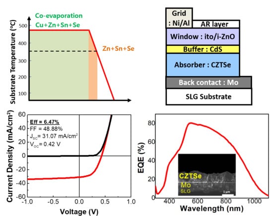
Figure 1. Growth temperature profile for Cu2ZnSnSe4 (CZTSe) film deposition.
Energies 13 01316 g001
Figure 2. SEM surface and cross-sectional images of Cu2(Zn,Sn)Se4 films prepared at various growth temperatures: (a,b) 550 °C, (c,d) 480 °C, (e,f) 440 °C, (g,h) 380 °C, and (i,j) 330 °C.
Energies 13 01316 g002
Figure 3. (a) XRD patterns of CZTSe films prepared at various temperatures ranging from 380 to 480 °C and (b) magnified view of the XRD (112) peak of CZTSe films.
Energies 13 01316 g003
Figure 4. Raman spectra of the CZTSe films prepared at various growth temperatures ranging from 380 to 480 °C.
Energies 13 01316 g004
Figure 5. (a) Illuminated J-V curves and (b) EQE spectra for CZTSe films prepared at various growth temperatures ranging from 380 to 480 °C.
Energies 13 01316 g005
Figure 6. (a) Illuminated J-V curves and (b) EQE spectra for CZTSe films grown at 480 °C with and without anti-reflection coating (ARC).
Energies 13 01316 g006
Table 1. Summary of photovoltaic parameters of photovoltaic (PV) devices based on the CZTSe films prepared at various growth temperatures. The Voc deficit of Eg q Voc   was calculated with an estimated bandgap (Eg) from the EQE spectra fitting, as seen in Figure S1. The estimated bandgap (Eg) increased from 1.14 to 1.23 eV as the growth temperature of CZTSe film increased from 380 to 480 °C.
SampleEffi.
(%)
VOC
(V)
Jsc (mA/cm2)Fill Factor FF
(%)
RSh
(Ώ)
RS
(Ώ)
AJ0
(mA/cm2)
Voc deficit
(mV)
480 °C6.080.42530.7746.484166.72.023.111.8 × 10−4805
440 °C3.600.36322.8443.47109.91.981.343.9 × 10−3827
380 °C1.360.27417.7128.1545.232.113.771.4 × 10−3873
Table 2. Summary of the results derived from the CV and DLCP measurement of CZTSe PV devices. (NA: Free carrier density, NIF: Interface defect density, NB: Bulk defect density).
Sample NA (cm3)NIF (cm3)NB (cm3)Depletion Width (nm)
480 °C1.0 × 10163.0 × 10151.6 × 1016119
440 °C9.2 × 10162.2 × 10163.7 × 101664.7
380 °C5.6 × 10161.5 × 10171.3 × 101670.5

