Article

Renewable Energy Powered Plugged-In Hybrid Vehicle Charging System for Sustainable Transportation

by
Elangovan Devaraj
1,*,
Peter K. Joseph
1,*,
Thundil Karuppa Raj Rajagopal
2,* and
Senthilarasu Sundaram
3,*
1
School of Electrical Engineering, Vellore Institute of Technology, Vellore 632014, India
2
School of Mechanical Engineering, Vellore Institute of Technology, Vellore 632014, India
3
Environment and Sustainability Institute, University of Exeter, Penryn TR10 9EZ, UK
*
Authors to whom correspondence should be addressed.
Energies 2020, 13(8), 1944; https://doi.org/10.3390/en13081944
Submission received: 3 January 2020 / Revised: 5 April 2020 / Accepted: 7 April 2020 / Published: 15 April 2020
(This article belongs to the Section E: Electric Vehicles)

Abstract

:
Energy transformation by power electronic converters is not feasible without the efficient use of renewable energy. The article tries to extend the use of renewable energy to PHEV battery charging. In PHEV, the battery is one of the major sources of stored energy. The converter used for charging these batteries is of crucial concern. The paper addresses various challenges in designing a DC to DC converter for battery charging in DC bus. An optimized converter is designed to work with renewable energy sources to accomplish a high boost ratio, low input current ripple, low output voltage ripple, high power efficiency, and high power density. A combination of two interleaved boost converters is effectively used with the overlap time switching to achieve a high voltage boost ratio in forming the DC bus. Transformer isolation is used to increase reliability and boost ratio further. The secondary side employs a series-connected voltage doubler. The converter boosts an input voltage of 24 V to a range of 300–400 V. Simulation results have been obtained for a 300 W system. Simulation results are validated by a prototype implementation for a 250 W system. The converter is studied and analyzed for steady-state and transient state characteristics and the power efficiency obtained is 92.9%.

Graphical Abstract

1. Introduction

Owing to the exponential increase in the industrial revolution, the world has been confronting extremely difficult challenges of meeting the ever-increasing demand of fuel, preserving the natural energy resources from becoming depleted and keeping the environment from getting polluted. These challenges can be overcome by employing various courses viz. saving energy, sustainable consumption, the efficient transformation of energy from one form to another, efficient use of energy, and shifting the focus from the use of conventional energy resources to non-conventional and renewable energy resources. The use of conventional energy resources has been making an irreversible impact on the environment on a global level. The analysis and study of the energy have compelled the industries and the upcoming engineers to go on a never-ending quest for sustainable energy. The quest for energy is proceeding in a direction to not only match the ever-increasing demand of energy but also, vitally accomplishing it in a way without putting the environment in peril. One of the main contributors to the adverse impact on the environment is the automotive sector. The world census of vehicles has surpassed 1 billion back in 2010. The future trend of an increase in vehicle census [1] can be seen in Table 1. Today there are various forms of clean energy available, to answer to the demand of one of the most significant besiegers, the automotive sector. All the leading automotive companies have been obliged to indulge in steering their direction of research and development to more efficient hybrid electric vehicles. The pros and cons of combustion engine vehicles and electric vehicles are shown in Table 2.
All vehicles require high torque at low speed and low torque at high speed. One of the merits of an electric vehicle is that speed-torque characteristics are inherently provided by the electric motor, for which a special gear ratio assembly is employed in combustion engine vehicles. This gear ratio assembly is a major factor in the degradation of efficiency in the combustion engine vehicle. Another major merit of electric vehicles is that the efficiency of energy transmission to the wheels of the vehicles is 90%. The overall efficiency degrades to 76% due to standby losses, friction losses, drag losses. Still, the efficiency is much higher in the electric vehicle than that in the combustion engine vehicles.
Since the battery is the primary source of stored electrical energy in a hybrid vehicle, the research in the development of highly efficient hybrid electric vehicles comes across the challenge in developing a converter that is not only power efficient, but also time-efficient in charging of the battery. A vigorous study and research are going on in developing new, high power-efficient, high power-dense, compact battery chargers.

2. State of the Art

Present-day converter systems available for battery charging applications in PHEV are studied and analyzed considering their merits and demerits. 2-cell interleaved full-bridge isolated converter has been recommended in the past for PHEV battery charging. The converter enjoys the merits of high efficiency and effective control with the use of trailing edge modulation [1]. The converter employs 2-cell interleaved full-bridge inverter, making use of eight switches and increasing the overall losses. Moreover, the converter is working as the second stage in the battery charging system and can be better suited with a smaller number of switches.
Voltage fed isolated converter with ZVS proposed in [2] employs a single cell of the full-bridge inverter, with a reduced number of switches than the converter discussed in [1] but, has a limitation of the boost ratio it can provide to implement a DC bus link for battery charging. Moreover, the voltage fed converter has a limited range of duty cycles than that of the current fed converter. This converter is used to transform power at 400 V input to 200–450 V. The converter is not suitable for a high boost ratio.
A current fed dual active bridge, AC source isolated converter proposed in [3] has a very particular advantage of PFC. Power factor correction is an important issue to which the converter addresses by using a boost converter as the first stage, then a high-frequency inverter in the second stage connected to a transformer. A full-bridge converter is connected to the transformer secondary to get a DC output proposed in [3,4]. The major disadvantage of this converter is the same as discussed in [1], a huge number of switches. The converter uses twelve switches and three stages, degrading the efficiency of and control of the converter.
A very elaborate and scrutinized study of various DC to DC bi-directional topologies suited for PHEV application is provided in [5,6]. All the bi-directional converter topologies discussed in [5,6] have employed a full bridge on either side of the galvanic isolation. The topologies are discussed based on the advantages and disadvantages of each topology. Some of the advantages common to all topologies of bi-directional converters are, easier control owing to constant frequency operation. Whereas the major limitation is that converters are not designed for boost application. The converter work with an input voltage of 750 Vdc to achieve a variable output voltage between 300 V–600 Vdc. None of the converters discussed in [1,2,3,4,5,6] can be used as first stage power conversion preceded by a renewable energy source because of the huge switching losses and inadequate gain ratio. Whereas maintaining a high voltage at the converter end will help to minimize the conductor size [7] in PHEV charging system. This will result in a rugged construction of the charging unit.
A phase-shifted semi-bridgeless boost PFC converter proposed in [8] works with universal 240 Vrms AC input to convert it to 400 Vdc along with maintaining a rich power factor. It also compares its performance with the interleaved converter counterpart. The topology presented is very effective owing to its salient advantage of maintaining the power factor which is otherwise degraded in any of the AC-DC power conversions, the small number of switches, higher efficiency, current fed conversion, high boost ratio possible due to the phase shift switching technique and easy closed-loop control. However, the performance and efficiency of the converter applied to high power applications can be uncertain, owing to its non-isolated operation. Apart from these technologies, industries are working on different ways to increase the driving range of EVs. Other than increasing the battery size, a separate power source can be integrated into the driving system to serve the purpose. BMW has introduced a concept of Extended Range Electric Vehicles (EREV) recently [9]. In EREV, an auxiliary generator is used to deliver additional power supply to extend the driving range of EVs. By this method, battery capacity is not affected by extending the range.

3. Major Challenges

A novel converter proposed in the article uses a double interleaved boost in the first stage with one renewable energy source, a transformer in the second stage and finally a cascaded voltage doubler rectifier as shown in Figure 1. An interleaved boost converter is basically two boost converter made to operate in parallel by keeping a phase difference of 180º between the switching of the two corresponding switches.
Furthermore, as shown in Figure 1, a double interleaved concept employs two interleaved converters with a single source, making the source current equal to the sum of the four input inductor currents. This operation is achieved by a phase shift of 90° between the sets of switches of both the converters. This operation helps cancel out the ripple currents of input inductors and keep the source current ripple in the allowable range. In the second stage, the outputs of the two interleaved boost converters are fed to two transformers, who act as galvanic isolation as well as contribute to the voltage boost. The secondary of the transformer is fed to a cascaded voltage doubler rectifier as shown in Figure 1. The use of two interleaved converter and cascading them at the voltage doubler rectifier makes the size of the filter capacitor much smaller as the voltage ripple frequency is four times the operating frequency. Some major advantages of the proposed novel converter are discussed ahead. The proposed converter demonstrates its novelty in several aspects. The converter uses two interleaved boost converters, transformers, and a voltage doubler rectifier. All three stages contribute to the boost action, which ultimately gives a very high voltage boost ratio.
The concept of interleaving is applied four times, making the ripple frequency of the input current as well as output voltage four times the operating frequency. This gives a very important advantage of reducing the size of magnetic elements as well as the output filter capacitors. Moreover, the input current ripple value is very less owing to the cancellation of a certain portion of input inductor currents. This advantage holds vital when renewable energy sources are concerned, especially fuel cells. The number of switches used is very small considering the voltage boost ratio accomplished. This reduces switch conduction and switching losses improving efficiency. At the output side, two interleaved limbs are cascaded with a cascaded voltage doubler rectifier, which reduces the number of doubler capacitors. This helps to reduce the value of source inrush current of the converter. Therefore, the novel converter topology proposed in the article is inferred to be best suited for the efficient conversion of renewable energy.

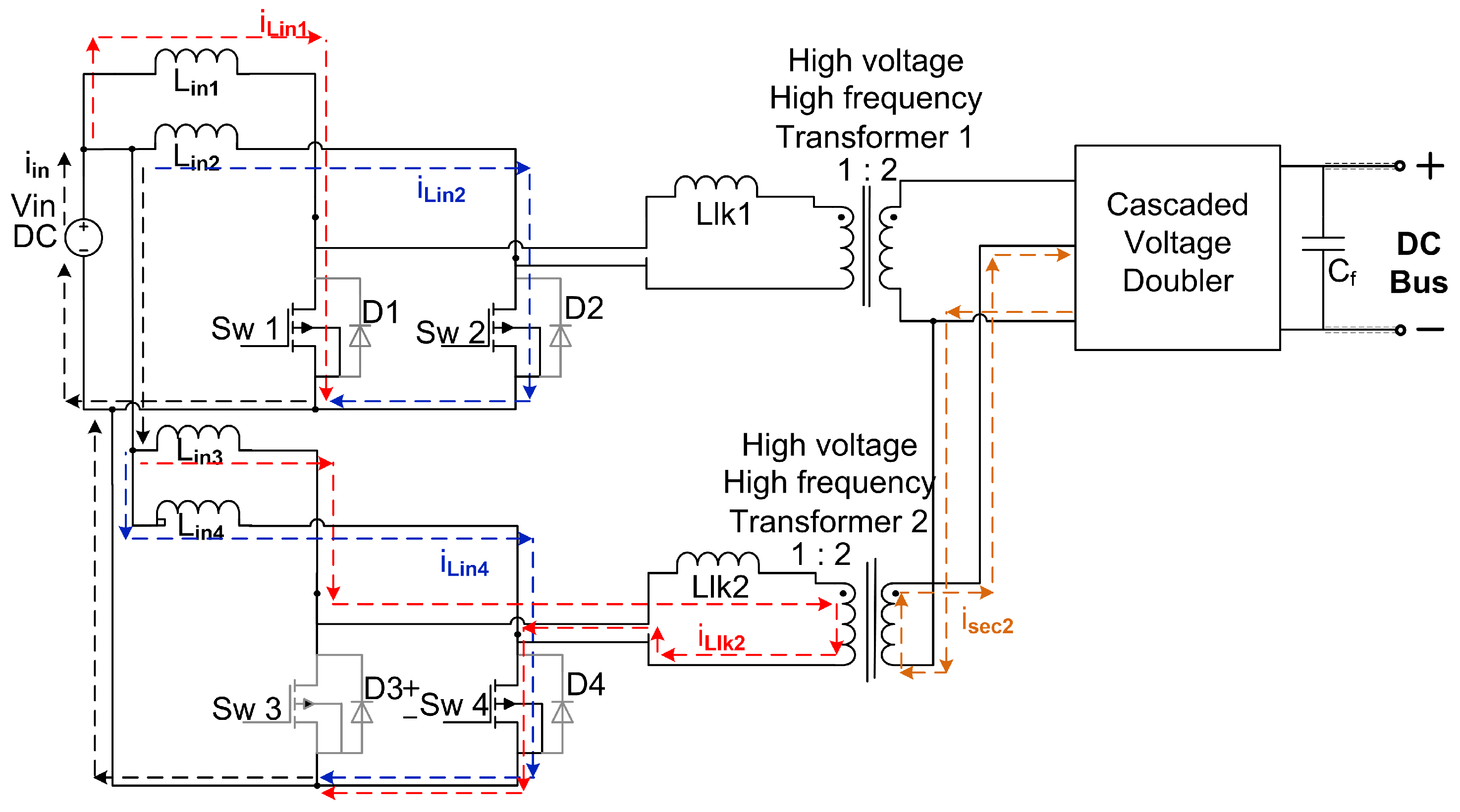
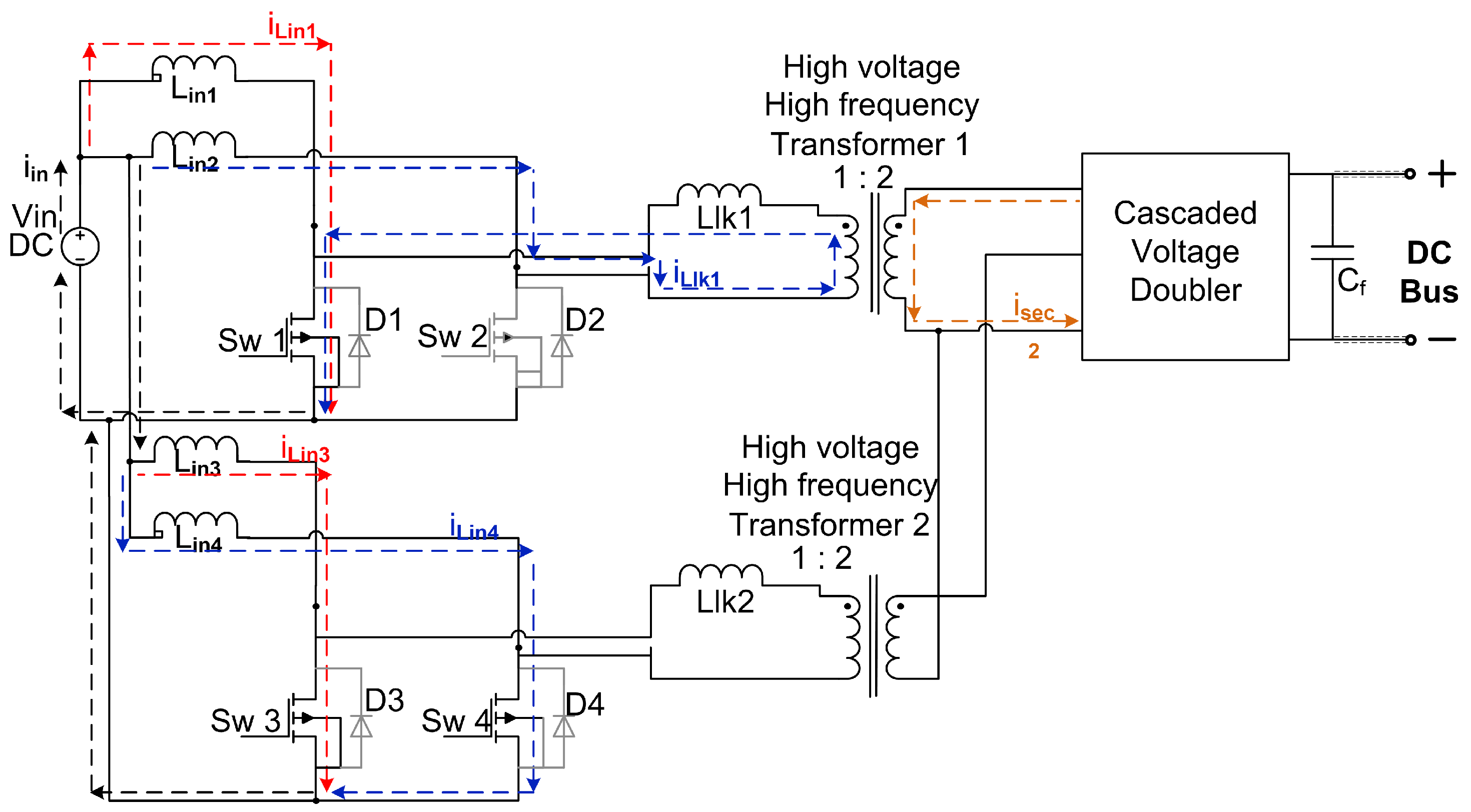
4. Operation of the Proposed Converter

4.1. Mode 1 ( t 0 t 1 )

The mode waveforms are shown in Figure 2. In this mode, switches Sw1, Sw2, and Sw4 are turned on at time instance t = t 0 and switch Sw3 is turned off. The current through the inductors Lin1, Lin2, and Lin4 increases while the current through inductor Lin3 starts decreasing. The switch current of Sw3 is diverted now to the transformer through the leakage inductor Llk2. The transformer in the second stage of interleaving is excited and the secondary current starts flowing in the direction shown in Figure 3.
The mode equations of Mode 1 are given underneath:
i L i n 1 ( t ) = V i n L i n 1 ( t t 0 ) + i L i n 1 ( t 0 )
i L i n 2 ( t ) = V i n L i n 2 ( t t 0 ) + i L i n 2 ( t 0 )
i L l k 1 ( t ) = 0
i s w 1 ( t ) = i L i n 1 ( t )
i s w 2 ( t ) = i L i n 2 ( t )
i L i n 3 ( t ) = V i n V p 2 L i n 3 ( t t 0 ) + i L i n 3 ( t 0 )
i L i n 4 ( t ) = V i n L i n 4 ( t t 0 ) + i L i n 4 ( t 0 )
i L l k 2 ( t ) = i L i n 3 ( t ) = V i n V p 2 L i n 3 ( t t 0 ) + i L i n 3 ( t 0 )
i s w 3 ( t ) = 0
i s w 4 ( t ) = i L i n 4 ( t ) + i L l k 2 ( t )

4.2. Mode 2 ( t 1 t 2 )

In this mode switches Sw1, Sw3 and Sw4 are turned on at time instance t = t 0 and switch Sw2 is turned off. The current through the inductors Lin1, Lin3, and Lin4 increases while the current through inductor Lin2 starts decreasing. The switch current of Sw2 is diverted now to the transformer through the leakage inductor Llk1. The transformer in the first stage of interleaving is excited and the secondary current starts flowing in the direction shown in Figure 4.
The mode waveforms are shown in Figure 2. The mode equations are given underneath:
i L i n 1 ( t ) = V i n L i n 1 ( t t 1 ) + i L i n 1 ( t 1 )
i L i n 3 ( t ) = V i n L i n 3 ( t t 1 ) + i L i n 3 ( t 1 )
i L i n 4 ( t ) = V i n L i n 4 ( t t 1 ) + i L i n 4 ( t 1 )
i s w 1 ( t ) = i L i n 2 ( t ) + i L l k 1 ( t )
i s w 2 ( t ) = 0
i L l k 1 ( t ) = i L i n 2 ( t ) = V i n V p 1 L i n 2 ( t t 1 ) + i L i n 2 ( t 1 )
i s w 3 ( t ) = i L i n 3 ( t )
i s w 4 ( t ) = i L i n 4 ( t )

4.3. Mode 3 ( t 2 t 3 )

In this mode switches Sw1, Sw2 and Sw3 are turned on at time instance t = t 0 and switch Sw4 is turned off. The current through the inductors Lin1, Lin2, and Lin3 increases while the current through inductor Lin4 starts decreasing. The switch current of Sw4 is diverted now to the transformer through the leakage inductor Llk2. The transformer in the second stage of interleaving is excited and the secondary current starts flowing in the direction shown in Figure 5. The mode waveforms are shown in Figure 2. The mode equations are given underneath:
i L i n 1 ( t ) = V i n L i n 1 ( t t 2 ) + i L i n 1 ( t 2 )
i L i n 2 ( t ) = V i n L i n 2 ( t t 2 ) + i L i n 2 ( t 2 )
i L i n 3 ( t ) = V i n L i n 3 ( t t 2 ) + i L i n 3 ( t 2 )
i L l k 2 ( t ) = i L i n 4 ( t ) = V i n V p 2 L i n 4 ( t t 2 ) + i L i n 3 ( t 2 )
i s w 1 ( t ) = i L i n 1 ( t )
i s w 2 ( t ) = i L i n 2 ( t )
i s w 3 ( t ) = i L i n 3 ( t ) + i L l k 2 ( t )
i s w 4 ( t ) = 0

4.4. Mode 4 ( t 3 t 4 )

In this mode, switches Sw2, Sw3, and Sw4 are turned on at time instance t = t 0 and switch Sw1 is turned off. The current through the inductors Lin2, Lin3, and Lin4 increases while the current through inductor Lin1 starts decreasing. The switch current of Sw1 is diverted now to the transformer through the leakage inductor Llk1. The transformer in the first stage of interleaving is excited and the secondary current starts flowing in the direction shown in Figure 6.
The mode waveforms are shown in Figure 2. The mode equations are given underneath:
i L l k 1 ( t ) = i L i n 1 ( t ) = V i n V p 1 L i n 1 ( t t 3 ) + i L i n 3 ( t 3 )
i L i n 2 ( t ) = V i n L i n 2 ( t t 3 ) + i L i n 2 ( t 3 )
i L i n 3 ( t ) = V i n L i n 3 ( t t 3 ) + i L i n 3 ( t 3 )
i L i n 4 ( t ) = V i n L i n 4 ( t t 3 ) + i L i n 4 ( t 3 )
i s w 1 ( t ) = 0
i s w 2 ( t ) = i L i n 2 ( t ) + i L l k 1 ( t )
i s w 3 ( t ) = i L i n 3 ( t )
The four modes of operation of the circuit explained above repeat again after every cycle of all four modes. The operation of the cascaded voltage doubler rectifier is similar to a single voltage doubler rectifier. The circuit of the cascaded VDR is shown in Figure 7.
During the positive half cycle of the first AC source diode, D1 conducts and charges capacitor C1. During the negative half cycle of the first AC source diode D2 conducts and charges capacitor C2. Similarly, during a positive half cycle of the second AC source which is 90° phase-shifted from the first source, the diode D3 conducts to charge C1 and during a negative half cycle, the diode D4 conducts to charge the capacitor C2. Each time, both the Capacitors are charged to the value Vm, which is the peak value of the AC voltages.

5. Steady State Analysis

5.1. Dc Voltage Gain Equation

The relation between the input voltage and the output voltage with the help of the duty cycle is given in the form of an equation. The equation gives the value of the average DC output voltage.
V o = 2 ( n s ) ( V i n ) ( 1 D )
Including the efficiency of the converter, the equation is given below:
P o u t = η P i n = V o u t 2 R l = η V i n I i n
V o = 2 ( η ) ( n s ) ( V i n ) ( 1 D )
where η is the efficiency of the system, D is the duty cycle, R l is the load voltage and n s is the secondary number of turns of transformer.

5.2. Input Inductor Design

Below the equation for input inductance is given. The main constraints in input inductor design are the allowable amount of ripple and the operating frequency. In the following equations, DC is the overlap duty.
L i n = ( D c ) ( V i n ) ( Δ i L i n ) ( f s )

5.3. VDR Capacitor Design

C v d r = P ( 1 D o ) ( V o ) 2 ( Δ V c v d r ) ( f t r a n s f o r m e r )
where P is the output power and DO is the overlap time of the pulses of one interleaved stage.

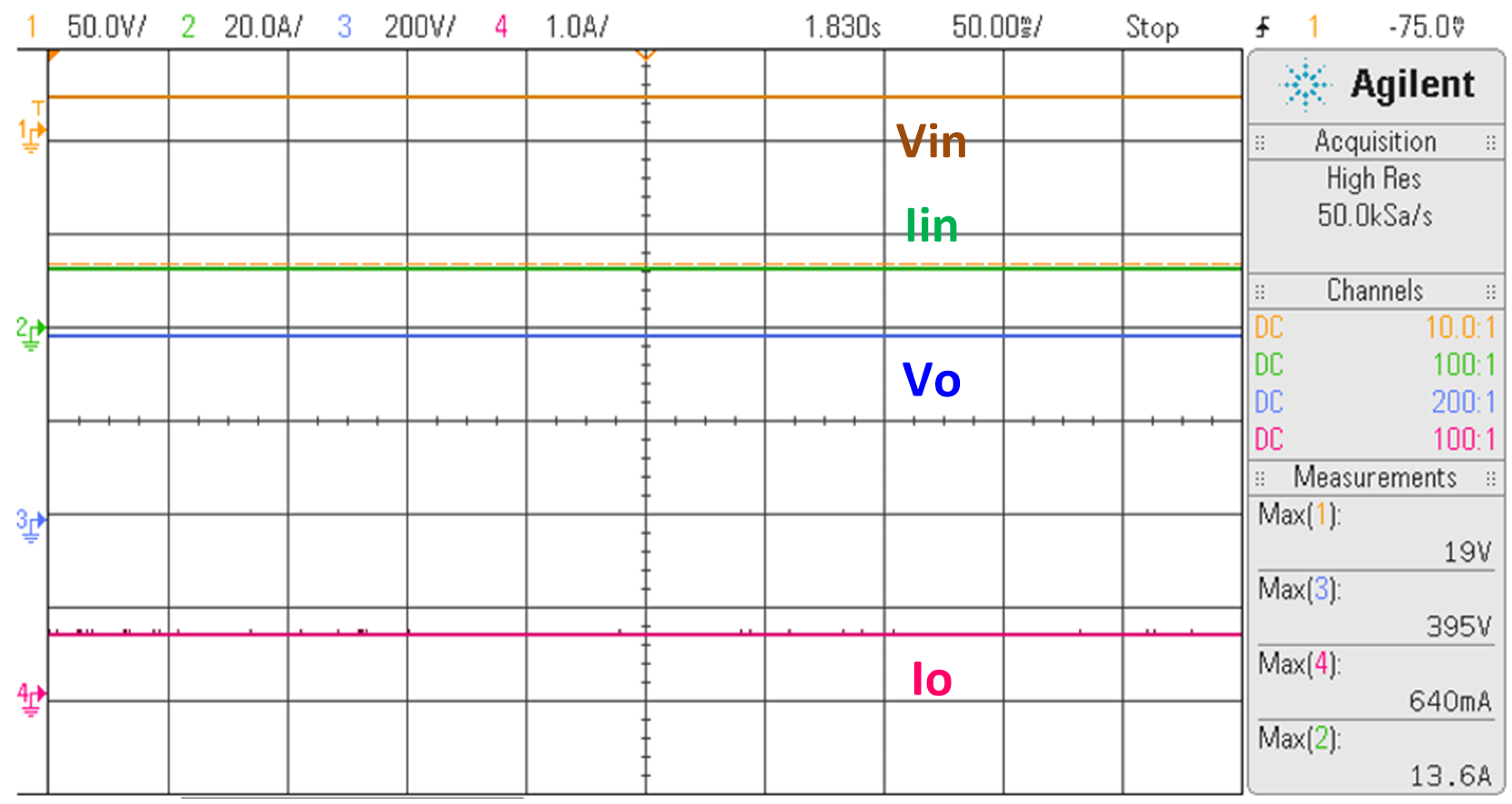
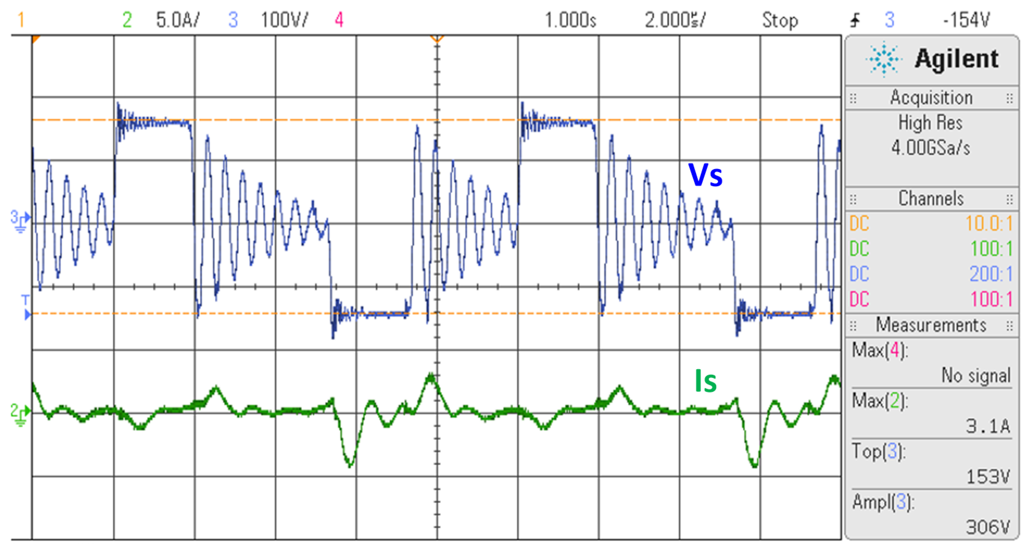
6. Experimental Implementation

6.1. Specifications

The specifications of the proposed system are as follows:
  • System Input voltage: 20 V–24 V
  • Switching frequency: 100 kHz
  • Output voltage: 300 V–400 V
  • Output power: 280 W
  • Output voltage ripple: <0.2%
  • Input current ripple: <1.2%

6.2. Component Specifications

The component specifications of the proposed system are as follows:
  • System Input inductor, Lin: 150 µH
  • Transformer turns ratio: 6 µH
  • Output voltage: 1:2
  • VDR capacitor: 1.2 µF
  • Output filter capacitor: 0.33 µF

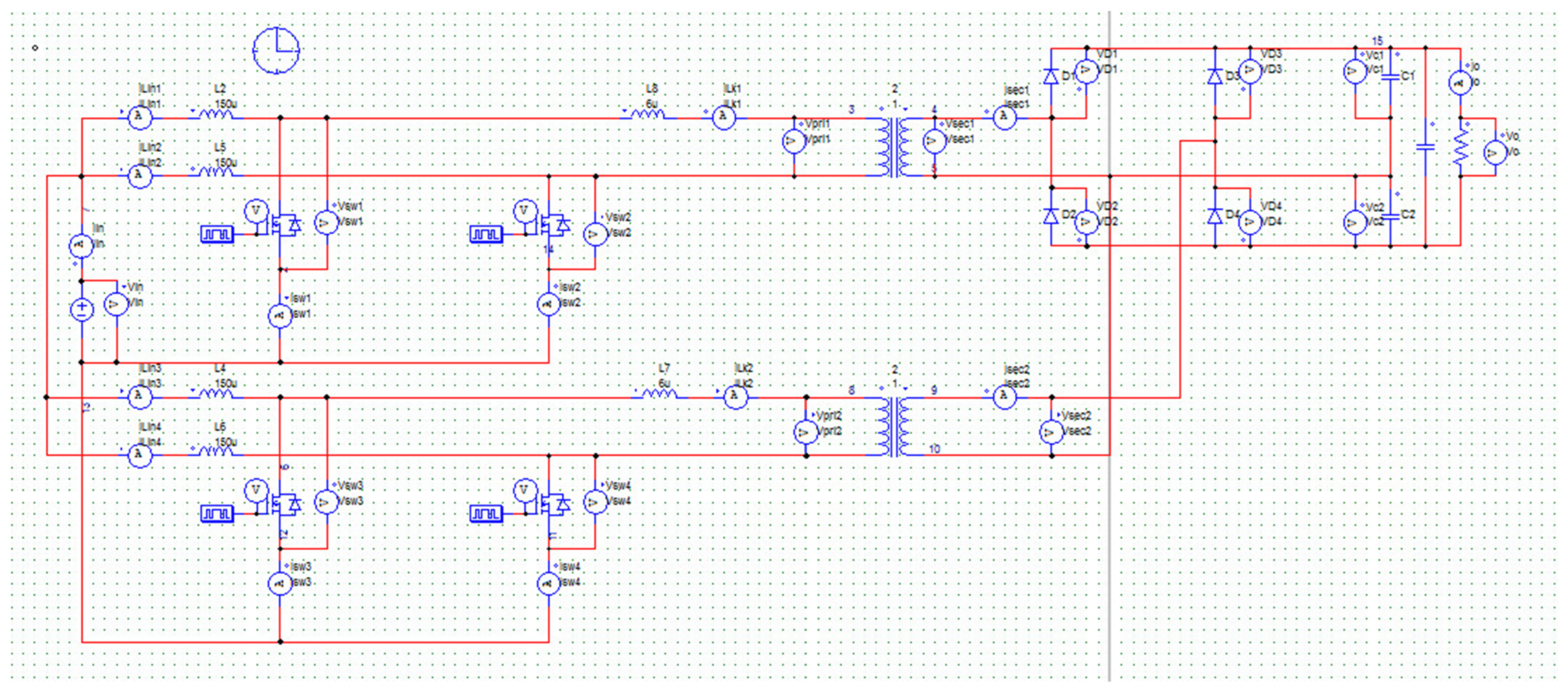
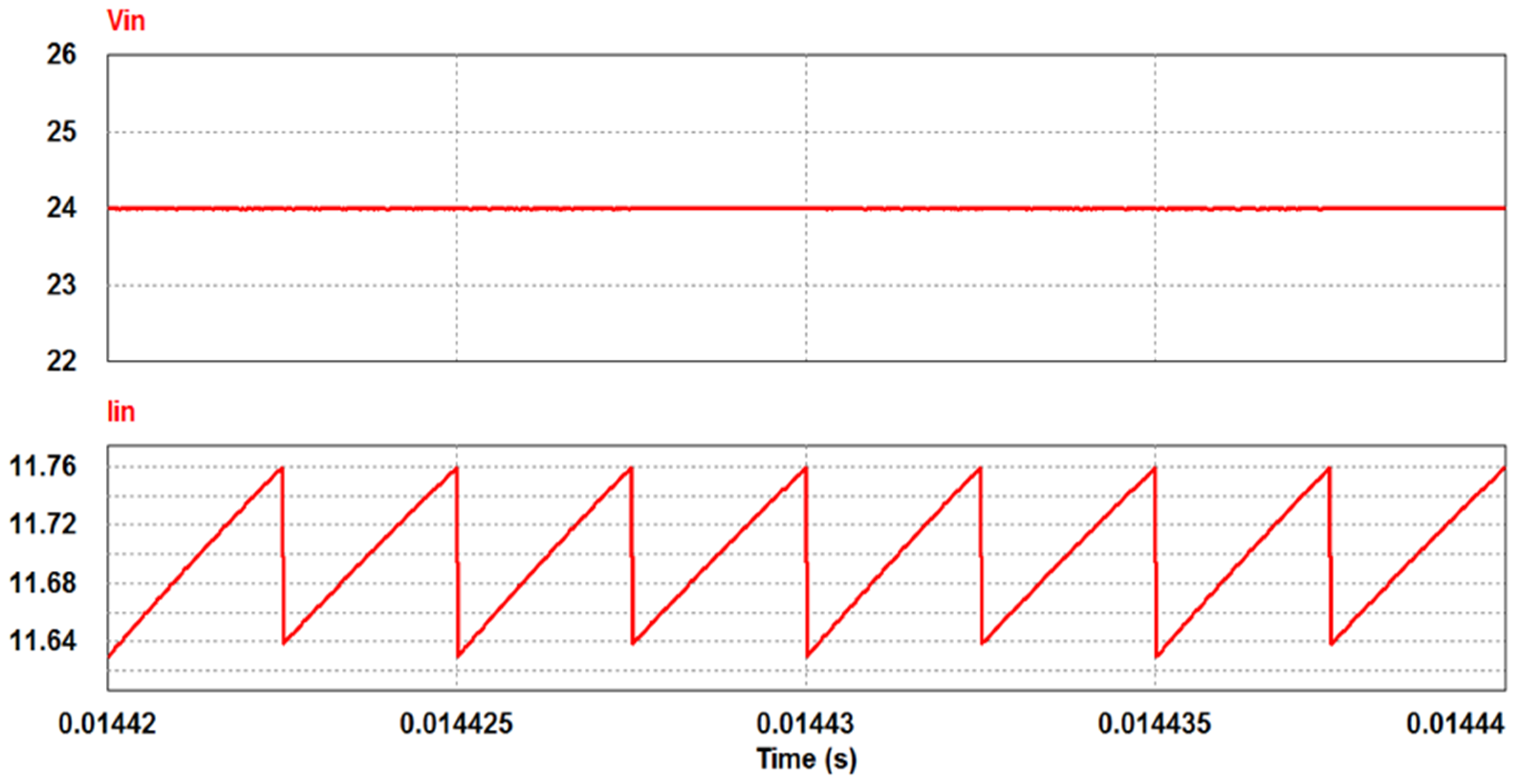
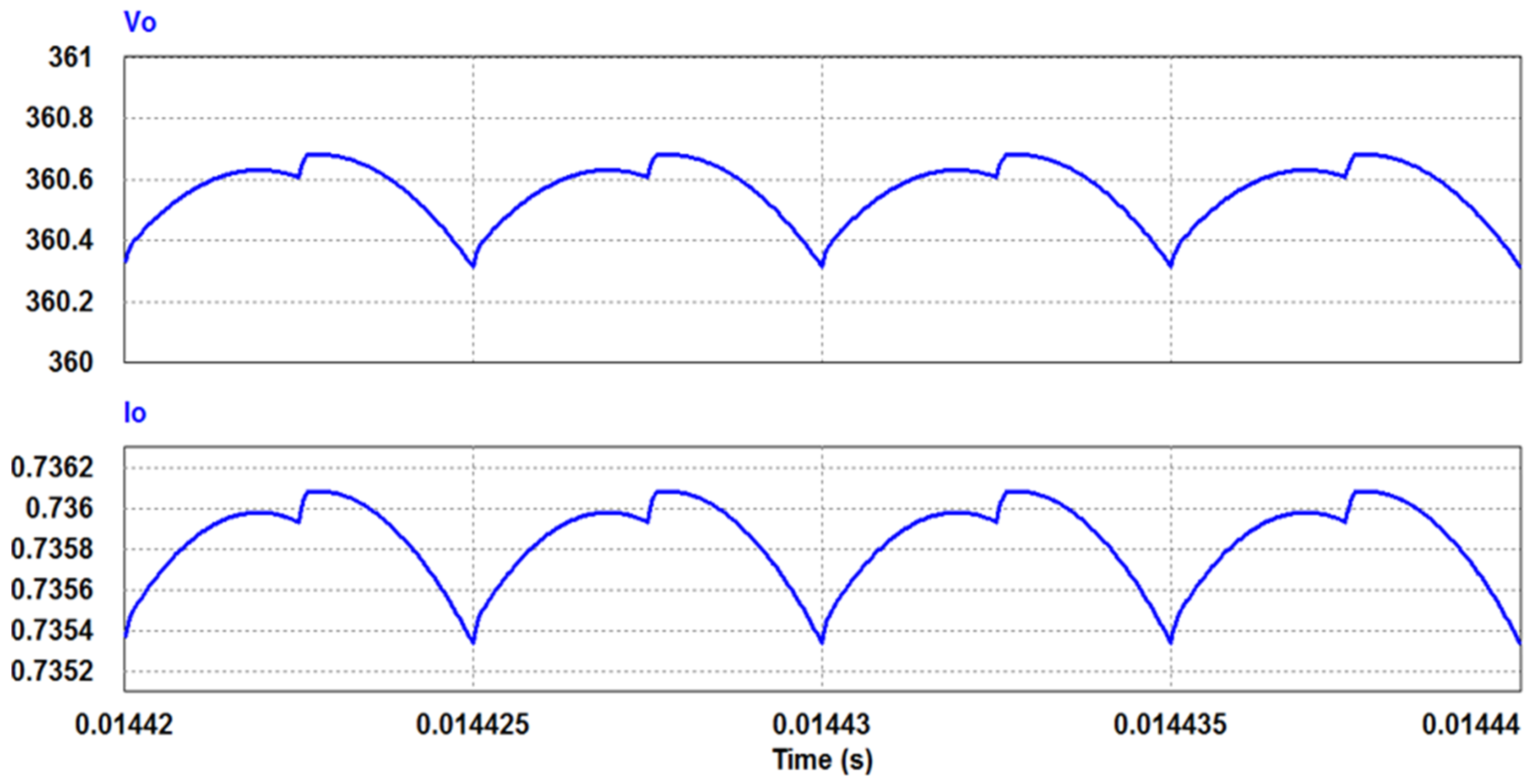
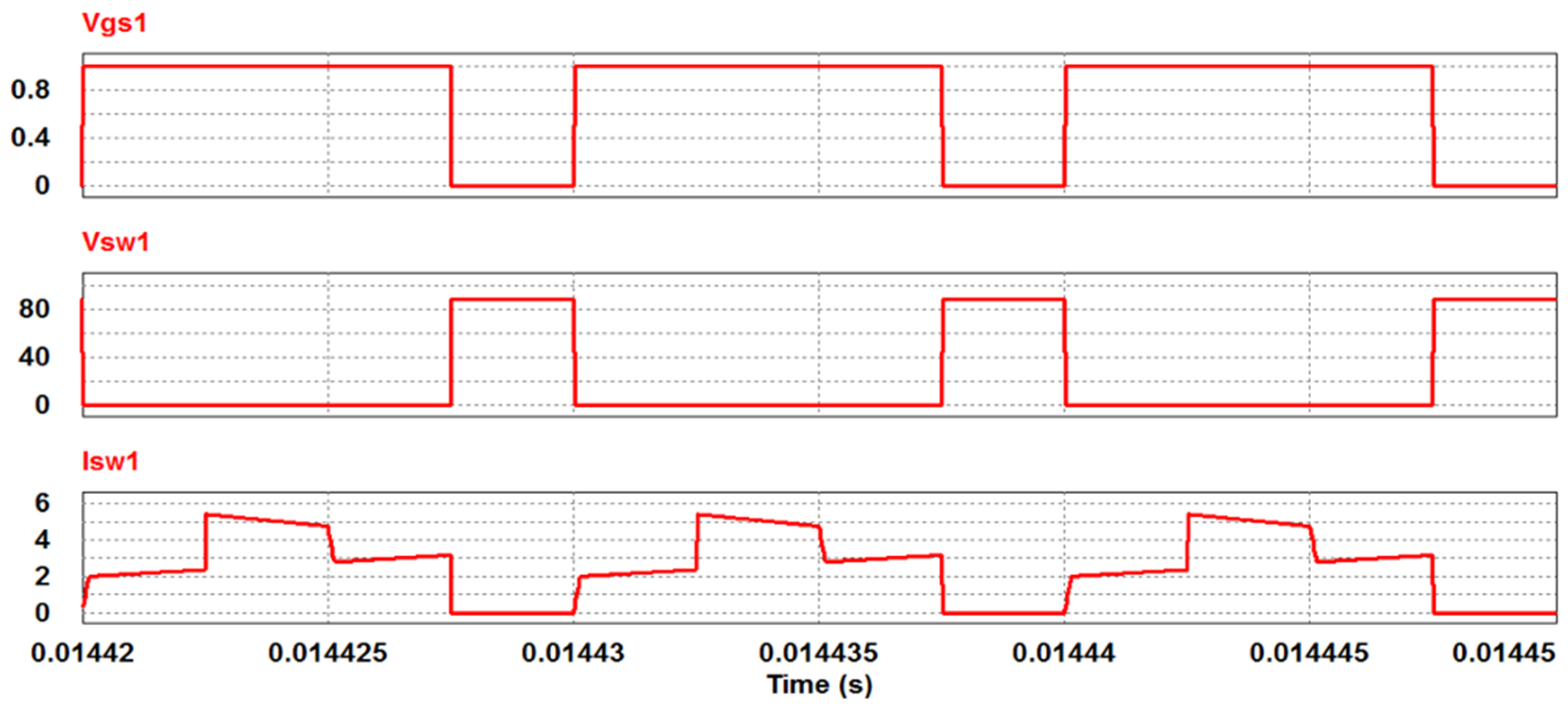
6.3. System Simulation

The PSIM simulation circuit is shown in Figure 8, after a thorough study and steady state analysis. The simulation is done with all the non-idealities, a particular component brings with it. Non-ideal parameters such as switch on state resistance, on state voltage drop, on state voltage drop of the anti-parallel diode and its bulk resistance is referred from the data-sheet of the selected hardware components. The transformer leakage inductance and the parameters mentioned before are set during simulation. This has helped to acquire the simulated results that are in a very close concurrence to the actual hardware results. The simulated circuit results are shown here.
The duty cycle used is 75%, for this simulation which can be extended up to 85%. Then come the input and output voltages and currents prominent in computation of the power efficiency to check if the topology is worth future realization. These results are shown in Figure 9 with input current ripple acquired to be below 1.2% of the average and Figure 10 shows output voltage ripple to be less than 0.2% of the average. Figure 11 and Figure 12 show the current through input side interleaved inductors. The current peak amplitudes for all four inductors are obtained to be almost equal corroborating the current sharing among all the four interleaved branches. This is important to accomplish maximum power from input to the output without much loss.
Figure 13 depict switch parameters, namely switch pulse, switch voltage and switch current. The current through all four switches is obtained to be fairly equal indicating current sharing. Figure 14 shows the leakage inductor currents of the two transformers.

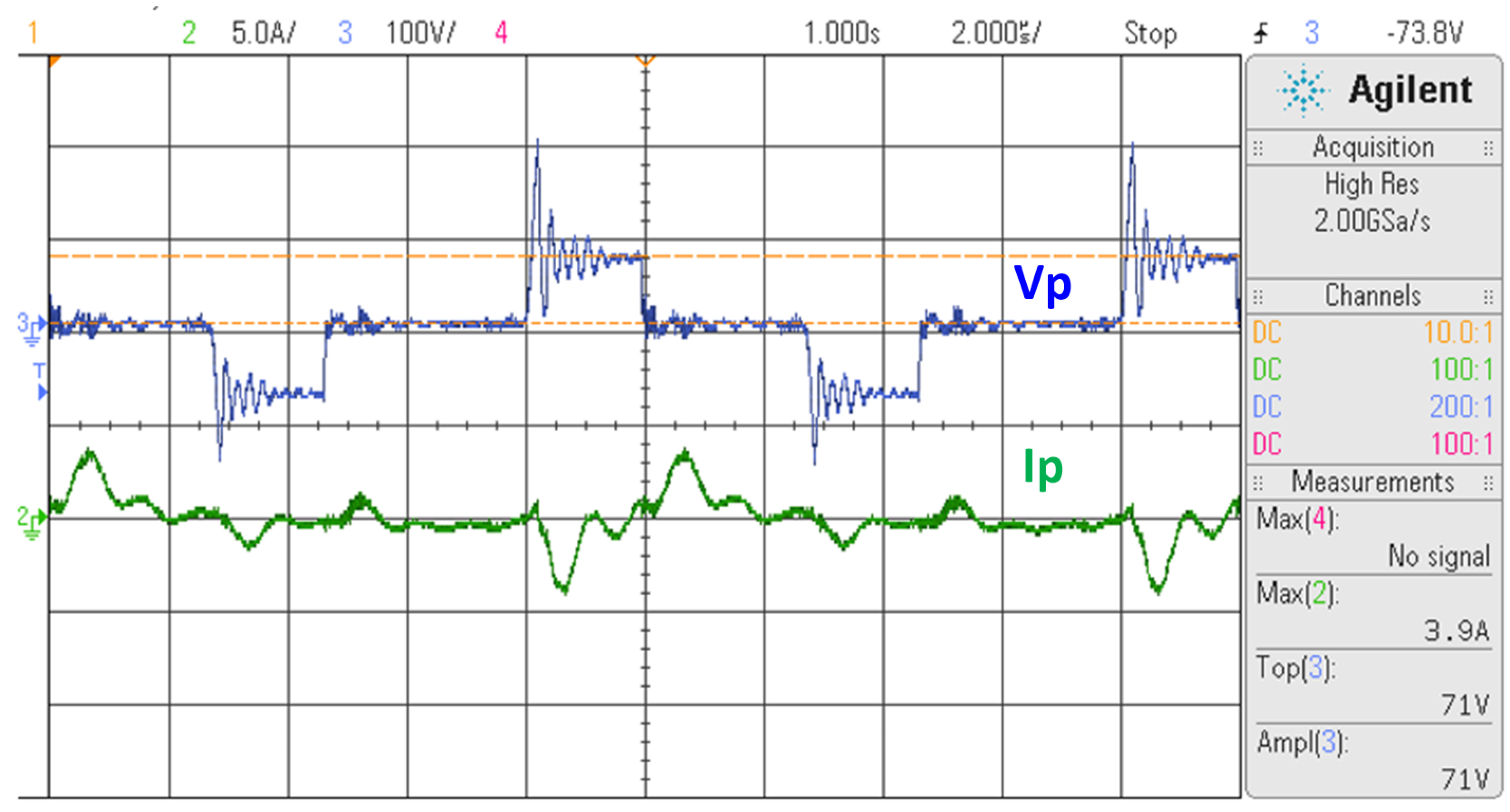
6.4. Hardware Implementation

The selected hardware specifications for the prototype are shown in Table 3. Since the proposed converter is bidirectional, there is a high voltage end and low voltage end present in the system during each operating mode. When the converter is in boost mode, the input is at low voltage end (source) and load is considered at high voltage end. Whereas in buck mode, the input is at high voltage end (source) and load is at low voltage end.
The implemented hardware is illustrated in Figure 15. Gate pulse pattern for switches is obtained from dSPACE and then given to Opto drivers which drive the output voltage. The amplified pulses are given to the switches of the converter.
The hardware setup is built for a power rating of 270 W. The switch gate-source voltage patterns are shown in Figure 16. Testing at input voltage at full load and excitation of 20 V is done, the results for input voltage and current along with output voltage and current were taken as shown in Figure 17. While taking the results of switch drain-source voltage and drain current, the drain-source voltage of the MOSFET was observed to exceed its allowable value, i.e., 200 V by a significant amount. While taking results for other parameters, the MOSFET went to break-down. Testing for 270 W was done for a short period of time, possible with the programmable power supply. Hence, for the remaining results, the hardware was tested extensively, at half the load condition for a long period of time. The results for input, output voltages, and currents taken at 130 W are shown in Figure 18 shows two patterns of current through input inductor. To show current sharing between two interleaved stages, the current through one input inductor from each stage is taken, on account of the availability of two current probes. The pattern of the inductor current could be similar to that in simulation result, had not been the MOSFET’s anti-parallel diode fell insufficient in its reverse recovery time and the tolerance in transformer leakage inductance. Figure 19 shows the switch gate-source voltage, drain-source voltage and drain current. Figure 20 shows the transformer primary voltage and current and Figure 21 shows transformer secondary voltage and current. Overall testing is done successfully at both half load as well as full load a condition.
The outcome of the implemented prototype is shown in Table 4. The efficiency at full load, of the novel converter topology proposed in the article is obtained to be 92.9% as can be seen from Figure 17 and Figure 18.

7. Conclusions

The current-fed converter and the voltage doubler rectifier helped to improve the boost ratio of the system from an input voltage of 20 V to an output voltage of 395 V. Both these features facilitated a low transformer turns ratio of 2. These phenomena helped to keep transformer non-idealities to a minimum extent. High-frequency operation at 100 kHz made magnetic elements smaller and compact, thereby increasing the power density of the 250 W system. The interleaving concept helped to suppress the input current ripple to a very low level. The current fed converter prevented the use of a source-side diode, which improved the overall efficiency by a factor of more than 5%. A novel converter topology was successfully designed, analyzed, simulated and tested with an efficiency of 93% in the prototype. Proposed converter topology is suitable for the conversion of renewable energy sources, for the PHEV battery charging application.

Author Contributions

E.D., and P.K.J., have developed the proposed research concept and they both are involved in circuit design, prototype implementation and circuit testing in the real-time environment. T.K.R.R., and S.S., shared his expertise in content management for the discussion and writing of the manuscript. All authors are to frame the final version of the manuscript as a full. Moreover, all authors involved in validating and to make the article error-free technical outcome for the set investigation work. All authors have read and agreed to the published version of the manuscript.

Funding

This research received no external funding.

Acknowledgments

We wish to acknowledge the “Royal Academy of Engineering”—Industry-Academia Partnership Programme IAPP-18-19/154 for partial funding of this research work. We would like to acknowledge Nachiket Chaudhari, Power Electronics Engineer, L&T Technology Services, Mumbai for the technical contributions to this work.

Conflicts of Interest

The authors declare no conflict of interest.

References

  1. Chakraborty, S.; Vu, H.N.; Hasan, M.M.; Tran, D.D.; Baghdadi, M.E.; Hegazy, O. DC-DC Converter Topologies for Electric Vehicles, Plug-in Hybrid Electric Vehicles and Fast Charging Stations: State of the Art and Future Trends. Energies 2019, 12, 1569. [Google Scholar] [CrossRef] [Green Version]
  2. Sayed, K. Zero-voltage soft-switching DC–DC converter-based charger for LV battery in hybrid electric vehicles. IET Power Electron. 2019, 12, 3389–3396. [Google Scholar] [CrossRef]
  3. Xue, L.; Shen, Z.; Boroyevich, D.; Mattavelli, P.; Diaz, D. Dual active bridge-based battery charger for plug-in hybrid electric vehicle with charging current containing low frequency ripple. IEEE Trans. Power Electron. 2015, 30, 7299–7307. [Google Scholar] [CrossRef] [Green Version]
  4. Kushwaha, R.; Singh, B. UPF-isolated zeta converter-based battery charger for electric vehicle. IET Electr. Syst. Transp. 2019, 9, 103–112. [Google Scholar] [CrossRef]
  5. Garcés Quílez, M.; Abdel-Monem, M.; El Baghdadi, M.; Yang, Y.; Van Mierlo, J.; Hegazy, O. Modelling, analysis and performance evaluation of power conversion unit in g2v/v2g application—A review. Energies 2018, 11, 1082. [Google Scholar] [CrossRef] [Green Version]
  6. Child, M.; Nordling, A.; Breyer, C. The impacts of high V2G participation in a 100% renewable Åland energy system. Energies 2018, 11, 2206. [Google Scholar] [CrossRef] [Green Version]
  7. Beachley, N.H.; Frank, A.A. Electric and electric-hybrid cars-evaluation and comparison. SAE Tech. Paper 1973, 1, 55–65. [Google Scholar]
  8. Kanimozhi, G.; Sreedevi, V.T. Semibridgeless Interleaved PFC Boost Rectifier for PHEV Battery Chargers. IETE J. Res. 2019, 65, 128–138. [Google Scholar] [CrossRef]
  9. BMW. Electric cars and plug-in hybrids explained. BMW Appl. Note 2020, 7, 1–6. [Google Scholar]
Figure 1. Expanded circuit diagram of the proposed converter.
Energies 13 01944 g001
Figure 2. Theoretical steady state waveforms of the proposed converter: (a) Boost converter waveforms; (b) High frequency transformer waveforms.
Energies 13 01944 g002
Figure 3. Mode 1 operation.
Energies 13 01944 g003
Figure 4. Mode 2 operation.
Energies 13 01944 g004
Figure 5. Mode 3 operation.
Energies 13 01944 g005
Figure 6. Mode 4 operation.
Energies 13 01944 g006
Figure 7. Cascaded voltage doubler rectifier.
Energies 13 01944 g007
Figure 8. Simulation Circuit in PSIM 9.1.1.
Energies 13 01944 g008
Figure 9. Input Voltage and current.
Energies 13 01944 g009
Figure 10. Output Voltage and Current.
Energies 13 01944 g010
Figure 11. Inductor currents ( I L i n 1 , I L i n 2 ).
Energies 13 01944 g011
Figure 12. Inductor currents ( I L i n 3 , I L i n 4 ).
Energies 13 01944 g012
Figure 13. Gate pulse, drain-source voltage and switching current.
Energies 13 01944 g013
Figure 14. Transformer Leakage Current.
Energies 13 01944 g014
Figure 15. Hardware prototype.
Energies 13 01944 g015
Figure 16. Switching gate-source voltages: Brown—switch 1, Green—switch 2, Blue—switch 3, Violet—switch 4.
Energies 13 01944 g016
Figure 17. Input-Output voltage and current waveforms: Brown— V i n , Green— I i n , Blue— V o , Violet— I o .
Energies 13 01944 g017
Figure 18. Input inductor currents (Green— I L i n 1 , Violet— I L i n 3 ).
Energies 13 01944 g018
Figure 19. Switching characteristics: Violet—gate voltage, Blue—drain-source voltage, Green—drain current, Brown—output voltage.
Energies 13 01944 g019
Figure 20. Transformer primary characteristics: Blue—Voltage, Green—current.
Energies 13 01944 g020
Figure 21. Transformer secondary characteristics: Blue—voltage, Green—current.
Energies 13 01944 g021
Table 1. Global vehicle ownership scenario.
Global Vehicle Ownership (Units in Million)
2010202020302035
Asia240401577686
North America263301336352
Latin America94157214233
OECD Europe372434485501
Middle East29456777
Africa26344552
Oceania18212425
Global Total1043139217471926
Table 2. Comparison of combustion engine vehicles and electric vehicles.
Sl. No.Comparison
Combustion Engine VehiclesElectric VehiclesFuel Cell Vehicles
1Longer Driving rangeShorter driving rangeLonger Driving range
2Refueling time is lessCharging time is moreRefueling time is less
3Low initial costHigh initial costHigh initial cost
4Running cost is highRunning cost is lowRunning cost is high
5Fuel tank to wheel efficiency is 25–30%Battery to wheel efficiency is 75–80%Fuel cell to wheel efficiency is 75–80%
6Noise pollutionNo noise pollutionNo noise pollution
7Requires gear assemblyDoes not require gear assemblyDoes not require gear assembly
8Pollutes the environmentPollution-free performancePollution-free performance
9Costly maintenanceEasy a cheaper maintenanceEasy a cheaper maintenance
10Complex controlEasy and smooth controlEasy and smooth control
Table 3. Comparison of combustion engine vehicles and electric vehicles.
ParameterSpecification
Input voltage (Boost mode)+25 V -0- −25 V
Output voltage (Boost mode)+100 V -0- −100 V (Line to line 200 V)
Input voltage (Buck mode)+80 V -0- −80 V
Output voltage (Buck mode)+20 V -0- −20 V
Frequency, Boost duty and buck duty50 kHz, 0.75 and 0.25
dSPACE kitDS 1104
Opto driverHCPL 3120
MOSFET SwitchIRF 640N, 200 V, 18 A
Fixed inductors (Ferrite core)2 mH
MKP capacitors20 µF
A resonant inductor (Ferrite core)35 µH
Resonant capacitor (MKP)2 µF
Table 4. Comparison of combustion engine vehicles and electric vehicles.
Sl. NoParameterSimulation ValuesPrototype Hardware ValuesUnits
1Designed Power Rating280272Watt
2Operating frequency100100kHz
3Input Voltage Range20–2420Volt
4Average Input current11.713.6Ampere
5Average output Voltage300–400395Volt
6Average output Current0.7–0.930.64Ampere
7Output Power Obtained264.6252.8Watt
Efficiency92.9%

