Article

Hybrid Tuning of a Boost Converter PI Voltage Compensator by Means of the Genetic Algorithm and the D-Decomposition

Department of Electrical Power Engineering, Faculty of Electrical Engineering, Wrocław University of Science and Technology, PL50370 Wrocław, Poland
*
Author to whom correspondence should be addressed.
Energies 2021, 14(1), 173; https://doi.org/10.3390/en14010173
Submission received: 13 December 2020 / Revised: 24 December 2020 / Accepted: 28 December 2020 / Published: 31 December 2020
(This article belongs to the Special Issue Modern Electrical Drives: Trends, Problems, and Challenges)

Abstract

:
In this paper the D-decomposition technique is investigated as a source of non-linear boundaries used with the Genetic Algorithm (GA) search of a PI voltage compensator gains of the boost converter operating in Continuous Conduction Mode (CCM). The well known and appreciated boost converter has been chosen as a test object due to its right-half plane zero in the control-to-output ( c 2 o ) voltage transfer function. The D-decomposition, as a technique relying on the frequency sweeping, clearly indicates not only the global stability but, in its extended version, regions satisfying the required gain (GM) and phase (PM) margins. Such results are in form of easy to interpret functions K I = f ( K P ) . The functions are easy to convert to the GA constraints. The GA search, with three different performance indexes as the fitness functions, is applied to a control structure with time delays basing on identified c 2 o voltage transfer functions. The identification took place in an experiment and in simulation. Outcomes of the identification are compared to mathematically derived formula taking into account certain parasitics. A complete set of practically useful mathematical formulas together with their validation in simulation and experiment is included.

1. Introduction

Power electronics circuits (PEC) are as popular as never before in this era of rapidly evolving miscellaneous solutions for electric energy production, processing and use [1,2]. Reasons and examples could be multiplied here. The first in mind could be a tandem of renewable energy sources with electric cars [3,4]. It is a tempting combination—already possible, although with some challenges [5]. Serious contributor to the challenge is not only the PEC hardware but also its indispensable control. Here the control is to be understood as not only the gate driver [6] but also as closed loop activities. They are strongly dependent on regulators with tunable parameters such as gains in case of widely used PID or PI schemes [7]. Proper selection of the gains sometimes may be a challenging task, especially when variety of different methods exists [8,9]. There may be somehow difficult decision to be made—which method should I use, does my theoretical background allow me to use it effectively, and so on. No simple answer is possible to such questions, although in this work one of possible paths is presented. The path seems to be quite intuitive although authors have not found it documented in literature for a boost converter. Therefore it is presented in this article in intelligible way as a complete guideline verified in practice.
In the era of relatively large and cheap computing power supported by miscellaneous embedded digital signal processing platforms based on Digital Signal Processors (DSP) or Field Programmable Arrays (FPGA) some help could come with a generic approach to control solutions design basing on: (i.) an identified open-loop plant transfer function of interest (this instead of analytically derived symbolic form), (ii.) control structure selection based on the transmittance model, and (iii.) intuitive gains selection guidelines dedicated to the control structure. This is not a new concept [10] but its implementation is still challenging. First of all, proper transfer function identification must take place [11]. It is done quite often with some compromises in terms of the transfer function order [12]. The compromises are driven by requirements about the plant model fidelity over certain frequency bandwidth. Once this is done a control structure can be built up around the plant [13]. In majority of PEC it may rely on the PID or PI regulators. In case of significant plant non-linearities, the regulators may be equipped with gains adjustment mechanisms such as the direct gain scheduling [14], the Fuzzy Logic membership-like scheduling [15,16] or the model predictive control [17]. Having passed these two steps one can start looking at proper gains selection. This last step normally calls for somehow advanced control theory [13,14], be it in the continuous or the discrete time domain, unless some heuristic methods are applied [18]. Among such methods one could think of well appreciated GA or Particle Swarm (PS) or even Cuckoo Optimization and few more [19,20]. Which one is the right one? An answer or rather a practical advice is in some way possible here the one which we understand and know the best. At this stage, even though we have chosen a method, there is still an open question—what is the quality of solutions found? The quality may be understood here as stability margin, let’s say in form of the GM and PM [21]. Here some quality indexes such as the IAE, or ITAE [22] and similar can be used as fitness functions but we basically still do not know about the exact margins. In such case something what could be compared to reverse engineering takes place. The solutions, let’s say PI controller gains, are tested and analysed. Then, if performance is not at satisfactory level, we search for new solutions with tuning settings of the search algorithm and/or changing our mathematical or simulation model. Sometimes it may be quite time consuming and frustrating process.
In such circumstances better solution would be to narrow down the search region. In other words, apply meaningful constrains. They could be in shape of the global stability region or even better a smaller region providing specific ranges of the GM and PM. Such constraints can be designated by means of the D-decomposition technique [23,24] relying on a frequency sweep test. The technique, in opposite to the classical Routh-Hurwitz criterion [25,26], allows for direct inclusion of time delays into analysis of control loops [27,28] which are always present in digital control solutions. The technique provides results which are easy in interpretation without advanced control theory knowledge. Quantitative results for common PI or PID compensator are derived basing on rather intuitive analyses of the characteristic polynomial of the closed loop transfer function. Somehow challenging may be here symbolic equations processing if one is looking for such a form of solution. Nevertheless for low order plants, let’s say two or three, with a PI compensator it is easy manageable by mathematical software such as e.g., Wolfram Mathematica—see solutions presented later in this article. In case of higher order plants numerical solutions are recommended. This may be considered as a sort of disadvantage of this technique but for relatively low order plants with PI compensators the computation times with nowadays PC can be counted in minutes, not in hours. This is still reasonable price to pay for such solutions.
As an alternative solution, claimed as less computing demanding and therefore faster, one could consider approach basing on Lyapunov stability criterion for the stable region indication presented in [29]. Perhaps at this stage such approach may be considered as a way to go in case of more complex systems, but rather not in case of single power electronics circuits with PI or PID compensators. Further research is also needed in area of time dalays inclusion in the proposed approach. In addition, the entry level in therms of mathematics is much higher when compared to the classical D-decomposition technique. This may represent some challenges while taking into account the GM and PM which is quite straight forward with the D-decomposition [24,27,28].
Consequently the GA with constraints calculated by means od the D-decomposition method has been chosen. The constrains were in form of the global stability boundary and the GM and PM driven boundary. Selected way has been verified by means of comparison with unconstrained GA results—this with the IAE, ITAE and ISTAE indexes used as minimized fitness functions. As a test object a well known dc-dc boost converter [30,31,32] operating in the CCM has been used—this with output voltage control. The circuit is employed in many of enumerated industrial applications, thus its performance during steady-state and transient is crucial [32]. Designing its control structure always calls for attention due to the fact that it is not only a non-linear object but has a right-half plane zero in its control-to-output transfer function [31]. This in reality, in closed loop control case, causes additional drop (within ON-time of switching cycle) of the output voltage in situation when the voltage starts falling do to e.g., change of load. In other words, the output voltage recovery process may start in consecutive switching cycle assuming no time delay in the feedback path. This is a physical explanation of this phenomena which is even more troublesome if a feedback path delays are present.
The motivation of this work was to verify contribution of the D-decomposition technique to basic GA optimization of PI voltage compensator gains of a physically built boost converter—this with three common quality indexes as fitness functions. All that as a physical proof of path leading to relatively simple and intuitive control design in power electronics.
The key contributions of this work could be described as:
  • intelligible indication of tangible path towards systematic design of PEC control solutions—this basing on practical example of a boost converter in the voltage mode control,
  • familiarization of this article reader with the D-decomposition technique and its possibilities in terms of not only the stability boundaries calculation but also indication of gains region quarantining particular GM and PM ranges,
  • use of the aforementioned boundaries as indication of the GA search constraints leading to better solutions with basic GA settings.
The paper is organized in five sections. Reasoning of this work is presented in the introduction. In the next section the boost converter as a verification circuit has been presented in format suitable for the conducted research. Practical aspects of mathematical modelling, simulation and identification are discussed in sufficient details. After that, usage of the D-decomposition technique to indicate the stability boundaries, and GM and PM requirements driven regions are shown in a complete and intelligible way. The regions are calculated basing on the c 2 o transfer functions identified in an experiment and in simulation. As next, the quality indexes are presented as fitness functions minimized by the GA. In the same section the GA search constrains are formulated basing on the outcomes the D-decomposition. Next section combines outcomes of the converter gains selection by means of the GA—this with and without constraints coming from the D-decomposition. All that has been verified in an experimental way and in simulation. The results are compared and discussed in this section. The conclusions and short outline for the future research are given in the last section.

2. Boost Converter as a Plant under Control

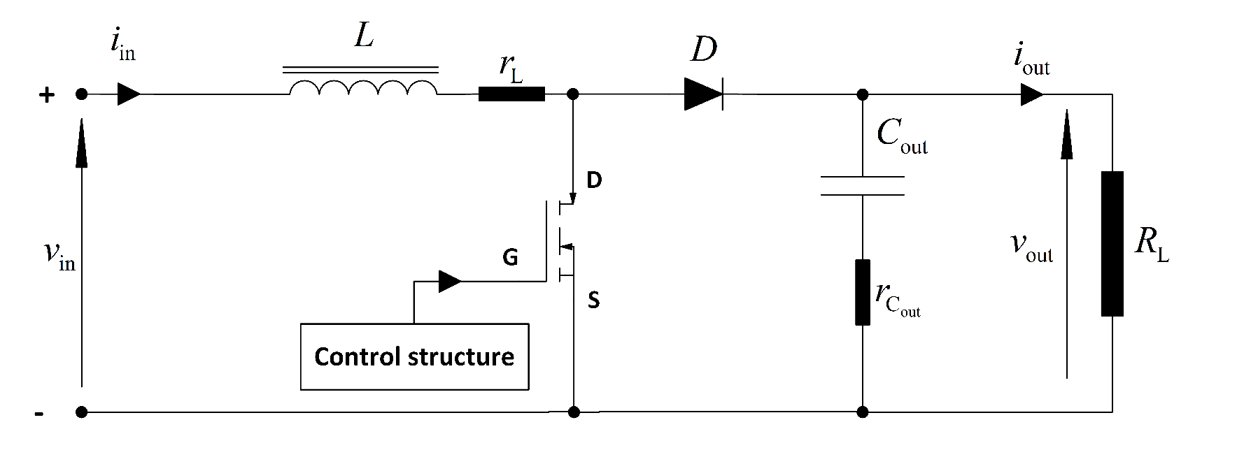
Circuit of a boost converter shown in Figure 1 was used as a plant under control. For simplicity reasons only its output voltage, v Boost , out , was under control—without the output current, i Boost , out , control. The v Boost , out in such circuit stays above its input voltage, v Boost , in , and is regulated by means of switching “ON” and “OFF” the semiconductor switch. In our case CoolMOS power MOSFET IXKN 75N60C was used. The switching is governed by a closed loop control scheme shown in Section 3.
The converter working at constant switching frequency operates in one of two operation modes. The CCM and the Discontinuous Conduction Mode (DCM). Generally speaking, main difference between this two modes is that within one switching cycle of the DCM the inductor current, i in , reaches zero for some time. The DCM enforces current increase form zero in every period of modulation. The CCM doesn’t allow the current to reach zero within the switching period and therefore the diode is being reverse biased when the switch is turned “ON” in every continuing cycle.
For purpose of conducted analysis, a Boost converter that operates in the CCM had been designed. Firstly, it was modelled in MATALB/Simulink environment. Secondly, an experimental set up was built. Modelling outcomes coming from Matlab are with superscript annotation . mat in this article and those from Simulink are with . sim . Experiment driven results are with . exp annotation. The analysed circuit parameters are shown in Table 1.
During modelling in Matlab the equivalent serial resistance of the inductance, r L , and the output capacitor, r C out , have been taken into account—this as easy available information and not excessively complicating the mathematical modelling. Simulink model, apart from the already mentioned parasitics, takes into account non-linear characteristics of the diode, D, and the MOSFET. The two models together with an experimental setup shown in Figure 2 contributed to development of c 2 o converter transfer functions which could be used during tuning of the voltage regulators.
In case of mathematical modelling in Matlab following transfer function was used [31].
P Boost mat , c , c 2 o ( s ) = v Boost , out mat , c ( s ) D ( s ) = P 0 z 1 + s z 0 s s 2 + a 1 s + a 0
where:
P 0 = r C out V Boost , in R out r C out + R out ( 1 D ) R out 2 2 r C out + R out + ( 1 D ) r C out R out r C out + R out + r L
a 0 = R out ( 1 D ) r C out + r L r C out + R out + ( 1 D ) R out 2 2 L · C out r C out + R out
a 1 = C out · R out ( 1 D ) r C out + r L r C out + R out + L L · C out r C out + R out
z 0 = ( 1 D ) 2 R out 2 r L r C out + R out L r C out + R out
z 1 = 1 C out r C out
and R out is the load resistance, D is the duty cycle, V Boost , in is the input voltage.
On basis of Equation (1) following transfer function of investigated plant has been obtained.
P Boost mat , c , c 2 o ( s ) = 0.37 s 2 + 1.48 · 10 4 s + 2.86 · 10 8 s 2 + 1.55 · 10 3 s + 4.53 · 10 6
Obtained transfer function corresponds to the duty cycle set point D = 35 % . The value is driven by the voltage conversion ratio equal to 1.5 . Remaining two c 2 o transfer functions, P Boost sim , est , c 2 o ( s ) for simulation and P Boost exp , est , c 2 o ( s ) for experiment, have been obtained by means of identification. The identification relied on analysis of step responses of the output voltage to the duty cycle, D, variation. The variation was also around the D = 35 % set point. It took place at rated input voltage, V in rtd = 30 V, rated output voltage V out rtd = 45 V and rated output power P Boost , out rtd = 80 W.
The overall circuit analysed in simulation can be seen in Figure 3. It contains the input filter stage in form of capacitance, C in , with its equivalent serial resistance r c , in . Such extension, when comparing to circuit shown in Figure 1, did not increase complexity of simulation but significantly increased accuracy of the outcomming transfer function. It will be discussed later in the paper.
Estimated c 2 o transfer function, basing on identification performed with simulation model, Figure 3, is as following.
P Boost sim , est , c 2 o ( s ) = 0.08 s 2 + 1.05 · 10 4 s + 1.82 · 10 8 s 2 + 1.12 · 10 3 s + 3.13 · 10 6
The last taken into consideration estimated c 2 o transfer function is one based on identification performed with an experimental circuit depicted in Figure 2. The circuit corresponds to schematic shown in Figure 3.
P Boost exp , est , c 2 o ( s ) = 0.47 s 2 + 1.97 · 10 4 s + 1.72 · 10 8 s 2 + 1.01 · 10 3 s + 2.95 · 10 6
The three estimated transfer functions represented by Equations (7)–(9) have been verified by means of comparison of their step responses, see Figure 4, and Bode plots, see Figure 5, this before using them for the control design purpose. While looking at Figure 4 one can see that the P Boost mat , c , c 2 o ( s ) , or rather v Boost , out mat , c , c 2 o , provides the fastest response although it significantly differs from the remaining two responses, v Boost , out sim , est , c 2 o ( s ) and v Boost , out exp , est , c 2 o ( s ) . The difference is driven by simplifications such as lack of the input filter stage and by not taking into account non-linear characteristics of the Diode and the MOSFET. Comparing results from the two remaining estimated transfer functions one can see that the plot based on P Boost sim , est , c 2 o ( s ) reflects sufficiently well the reality represented by P Boost exp , est , c 2 o ( s ) . Measurements from Simulink simulation and experiment have been shown as an additional proof of identifications performed. The experimentally measured v Boost , out exp , m , c 2 o was recorded with an oscilloscope and exported to the Matlab as data in the .csv file format.
Corresponding Bode plots can bee seen in Figure 5. In low to medium frequency range they intuitively reflect the time domain results from Figure 4. In higher frequency range the P Boost mat , c , c 2 o ( s ) reflects the theory [30] while the P Boost sim , est , c 2 o ( s ) and P Boost exp , est , c 2 o ( s ) somehow reflect the real circuit exposed to parasitics interactions and limited measurement capabilities during identifications. Despite of the phase differences the two former transfer functions have been selected for further investigations. Mathematically derived P Boost mat , c , c 2 o ( s ) was dropped off as one not imitating all parasitic phenomena present in the real plant.

3. Designation of Desired Output Voltage Compensator Gains Boundaries by Means of the D-Decomposition Technique

Before entering the gains selection stage, with use of a Genetic Algorithm, two boundaries limiting set of possible solutions were elaborated. Both of them were calculated by means of the D-decomposition proposed by Neimark in 1948 [23]. This technique in its original assumption establishes direct correlation between the nth-order characteristics equation and the space of permissible parameters (e.g., compensator gains) for which the stability condition is fulfilled. It is possible to signify a parametric surface D ( l , r = n l ) in such equation. The l and r represent number of the equation roots in the left and right half-plane respectively. If l = n then there is no roots in the right half-plane, r = 0 . Therefore the surface D ( l = n , 0 ) indicates stable region. The stable region can be calculated basing on substitution of s = j ω in the characteristic equation. The ω = 2 π f belongs to real numbers R , in range ( , + ) . Equating to zero the real and imaginary parts of obtained equation leads to dependencies describing parametric hypersurface which precisely designates the stability boundary in the D surface if r = 0 .
Additionally, it is necessary to find out which side of the boundary is the stable region. In case of two changing parameters such as the PI compensator gains one more boundary is needed. It is achieved by introducing a Δ D 0 ( m 2 ) -dimensional hyperplane. The Δ D 0 hyperplane is related to the characteristic equation by means of a real zero at the origin of the s-plane ( s = 0 ) . Solution of such equation provides a complementary criterion supporting indication of the second parameter region.
Described technique has been further extended to facilitate allocation of desired GM and PM. Shortly speaking, it can be achieved by replacing the point 1 + j 0 with a complex number representing the GM or PM.
For purpose of symbolic equations formulation a closed loop control structure shown in Figure 6 is considered. Apart from a controller and plant transfer functions it contains time delays driven by Pulse Width Modulation (PWM) section ( τ PWM ) and Analog-to-Digital (A2D) conversion ( τ A 2 D ) together with a low pass filter F ( s ) .
The closed-loop transfer function describing control structure shown in Figure 6 can be written as following:
G CL ( s ) = Y ( s ) R ( s ) = C ( s ) e s τ PWM P ( s ) 1 + C ( s ) e s τ PWM + τ A 2 D P ( s ) F ( s )
where: R ( s ) is a reference signal; C ( s ) is a controller transfer function (PI in this case); P ( s ) is a plant transfer function (boost converter in this case); Y ( s ) is the plant output (output voltage of the boost converter).
Taking in to account the boost converter c 2 o transfer functions expressed by Equations (7) to (9) it is possible to formulate following general formula for such plant:
P ( s ) = b 2 s 2 + b 1 s + b 0 s 2 + a 1 s + a 0
Transfer function of the filter can be written as:
F ( s ) = 1 s τ F + 1
The PI controller with its proportional, K P , and integral, K I , gains can be written as:
C ( s ) = K P + K I s
In such case the closed-loop transfer function Equation (10) can be rewritten as:
G CL ( s ) = e s τ A 2 D s K P + K I b 2 s 2 + b 1 s + b 0 ( s τ F + 1 ) s 4 C 1 + s 3 C 2 + s 2 C 3 + s C 4 + C 5
where:
C 1 = e s τ PWM + τ A 2 D τ F
C 2 = e s τ PWM + τ A 2 D + b 2 K P + e s τ PWM + τ A 2 D a 1 τ F
C 3 = e s τ PWM + τ A 2 D a 0 τ F + b 1 K P + b 2 K I + e s τ PWM + τ A 2 D a 1
C 4 = e s τ PWM + τ A 2 D a 0 + b 1 K I + b 0 K P
C 5 = b 0 K I
The characteristic equation of Equation (14) in general form, in the frequency domain ( s = j ω ) , can be written as a function of three arguments:
G OL ( j ω , K P , K I ) = 1 + j 0
here the 1 + j 0 instead of 1 only is written to emphasize that the imaginary part exists although is equal to zero. At this stage we could derive formulas for the K P and K I in function of the ω . It would indicate part of the global stability boundary. This combined with outcomes of the Δ D 0 condition represented in this case as:
Δ D 0 b 0 K I = 0
would completely describe the glogal stability boundary. Nevertheless, we can do it later on with extended formulas taking into account requirements for the GM and PM—equal to 0 in such case.
Moving towards implementation of requirements for certain GM or PM—the point ( 1 , j 0 ) will become now a complex number and therefore the generalized Equation (15) can be written as following:
G OL ( j ω , K P , K I ) = a + j b
where a + j b stands for coordinates of an arbitrary point in the polar plane.
The Equation (17) can be split as following:
Re = [ G OL ( j ω , K P , K I ) ] = a
Im = [ G OL ( j ω , K P , K I ) ] = b
Location of the point in Nyquist plot can be represented by complex numbers z ̲ GM = a GM + j b GM and z ̲ PM = a PM + j b PM corresponding to certain GM and PM respectively.
Value of the GM in dB by virtue of its definition leads to following real and imaginary parts of the complex number z ̲ GM :
a GM = 10 G M 20 b GM = 0
Similarly the PM, in d e g , leads to following formulas:
a PM = cos 2 π P M 360 + π b PM = sin 2 π P M 360 + π
Basing on Equation (17) with reference to Equation (20) the K P and K I gains as functions of frequency and required GM can be calculated as following:
K P ( ω , GM ) = b 1 ω a 0 ω + a 1 τ F ω 3 + ω 3 C 7 + ω 2 τ F a 0 ω 2 + a 1 C 6 + 10 GM 20 1 ω b 0 2 2 b 0 b 2 ω 2 + b 1 2 ω 2 + b 2 2 ω 4 ω b 0 b 2 ω 2 a 0 ω 2 ( a 1 τ F + 1 ) C 6 ω τ F a 0 ω 2 + a 1 C 7 ω b 0 2 2 b 0 b 2 ω 2 + b 1 2 ω 2 + b 2 2 ω 4
K I ( ω , GM ) = ω C 7 a 0 b 0 + ω 2 ( b 1 τ F b 2 ) + ω 2 b 0 ( a 1 τ F + 1 ) + a 1 b 1 + b 2 τ F ω 2 + ω 2 ( b 2 b 1 τ F ) + C 6 b 0 2 2 b 0 b 2 ω 2 + b 1 2 ω 2 + b 2 2 ω 4 + ω 2 ω 2 a 0 b 0 τ F + b 1 + b 2 τ F ω 2 + a 1 b 0 + ω 2 ( b 1 τ F b 2 ) + 10 GM 20 10 GM / 20 1 b 0 b 2 ω 2 b 0 2 2 b 0 b 2 ω 2 + b 1 2 ω 2 + b 2 2 ω 4
In the same way, substituting in Equation (17) formulas from Equation (21) representing the PM requirements leads to following equations:
K P ( ω , P M ) = b 1 ω ω 3 ( a 1 τ F + 1 ) a 0 ω C 7 + ω 2 τ F a 0 ω 2 + a 1 C 6 + cos π PM 180 1 ω ( b 0 2 2 b 0 b 2 ω 2 + b 1 2 ω 2 + b 2 2 ω 4 ) b 0 b 2 ω 2 ω 2 τ F a 0 ω 2 + a 1 C 7 + ω a 0 ω 2 ( a 1 τ F + 1 ) C 6 + sin π PM 180 ω ( b 0 2 2 b 0 b 2 ω 2 + b 1 2 ω 2 + b 2 2 ω 4 )
K I ( ω , P M ) = ω 2 C 6 ω 2 a 0 b 0 τ F + b 1 + b 2 τ F ω 2 + a 1 b 0 + ω 2 ( b 1 τ F b 2 ) b 1 ω sin π PM 180 b 0 2 2 b 0 b 2 ω 2 + b 1 2 ω 2 + b 2 2 ω 4 + cos π PM 180 b 2 ω 2 b 0 + b 0 b 2 ω 2 + a 0 b 0 ω C 7 b 0 ω 3 C 7 + a 1 b 1 ω 3 C 7 a 0 b 2 ω 3 C 7 b 0 2 2 b 0 b 2 ω 2 + b 1 2 ω 2 + b 2 2 ω 4 + a 0 b 1 τ F ω 3 C 7 a 1 b 0 τ F ω 3 C 7 + a 1 b 2 τ F ω 5 C 7 b 1 τ F ω 5 C 7 + b 2 ω 5 C 7 b 0 2 2 b 0 b 2 ω 2 + b 1 2 ω 2 + b 2 2 ω 4
where:
C 6 = cos ω ( τ PWM + τ A 2 D )
C 7 = sin ω ( τ PWM + τ A 2 D )
Formulas represented by Equations (22)–(25), combined with Equation (16), can now be used to visualize the global stability boundary (GM = 0 dB in Equations (22) and (23) or PM = 0 in Equations (24) and (25)) or regions related to required margins values. Such formulas, which in the past could be considered as relatively complex parametric formulas, nowadays can be easily computed with Matlab or different software running on a standard PC. In our case the Wolfram Mathematica was used. It took about 30 s to derive (process) the formulas. Results with P Boost sim , est , c 2 o ( s ) according to Equation (8) can bee seen in Figure 7.
While looking at Figure 7, one should notice that area of the K P and K I gains fulfilling requirements of desired GM and PM is significantly smaller when compared to the global stability area. This small area is comparable with size of its equivalent obtained for P Boost exp , est , c 2 o ( s ) according to Equation (9), see Figure 8. In both cases the GM and PM were the same, GM 10 ; 25 dB and PM 80 ; 90 . While comparing the overall stable regions, one can see that in case of experimental c 2 o transfer function the area is bigger.

4. Selection of the Performance Indexes and Constrains for the Boost Converter Gains Search with  GA

Having the scheme of closed loop control system shown in Figure 6, it is necessary to find proper K P and K I gains. Overall control quality could be then evaluated on a basis of assessment of the converter output voltage response to the reference step change. It was assumed in this article to suppress the overshoot, as well as to shorten the rise time as much as possible. Therefore three following performance indexes were used—this for the sake of comparison process.
I A E = 0 t sim | e ( t ) | d t
I T A E = 0 t sim t | e ( t ) | d t
I S T A E = 0 t sim t 2 | e ( t ) | d t
where: IAE is the Integral of Time Absolute Error; ITAE is the Integral of Time multiply Absolute Error; ISTAE is the Integral Square of Time multiply Absolute Error; t sim is the simulation time; e ( t ) is the error value in time.
The performance indexes were used directly as the GA minimized fitness functions. Additionally, in case of the GA constrained search, following constrains were applied with x 1 and x 2 , ( x 1 , x 2 ) R 2 , standing for the K P and K I respectively:
x 1 > 0 x 2 > 0 x 2 1202.0849 x 1 2 + 904.6544 x 1 + 18.7498
for simulation model based on the global stability boundary shown in Figure 7.
x 1 > 0 x 2 > 0 x 2 5319.6902 x 1 4 5964.4032 x 1 3 2241.4153 x 1 2 + 956.2346 x 1 + 17.0480
for experimental model based on the global stability boundary shown in Figure 8.
x 1 > 0 x 2 > 0 x 2 425371.4450 x 1 4 93263.1504 x 1 3 34760.4443 x 1 2 + 890.9319 x 1 + 5.8412 x 2 373087646.4618 x 1 4 5310855.6771 x 1 3 1.03987 . 4167 x 1 2 + 1879.7387 x 1 + 6.3527 x 2 75642928.2340 x 1 4 2949239.7717 x 1 3 195472.3433 x 1 2 + 890.9319 x 1 2 + 1.0387 x 2 3609723992.6768 x 1 4 + 41458061.6942 x 1 3 276418.4587 x 1 2 + 2783.5193 x 1 2 0.2073
for simulation model based on the boundary set up by constrains GM 10 dB ; 25 dB and PM 80 ; 90 —shown in zoom in Figure 7.
x 1 > 0 x 2 > 0 x 2 168223.3746 x 1 4 59644.0315 x 1 3 7108.7978 x 1 2 + 956.2346 x 1 + 5.3911 x 2 187337820.5329 x 1 4 8901551.76966 x 1 3 184878.5782 x 1 2 + 2040.3047 x 1 2 + 7.4525 x 2 29914816.3250 x 1 4 1886109.8851 x 1 3 39858.6274 x 1 2 + 956.2346 x 1 2 + 0.9587 x 2 1017897508.7794 x 1 4 142554430.1617 x 1 3 45012.8727 x 1 2 + 2883.8696 x 1 2 0.0240
for experimental model based on the boundary set up by constrains GM 10 dB ; 25 dB and PM 80 ; 90 —shown in zoom in Figure 8.

5. Selection of the Boost Converter Gains by Means of GA with Hints from the D-Decomposition Technique

Overall optimization works were divided into three actions—each taking into account the performance indexes according to Equations (26)–(28). Firstly, unconstrained GA search was conducted. Secondly, GA was constrained with the global stability regions indicated by dashed lines in Figure 7 for simulation and in Figure 8 for experiment. The regions were calculated by means of the D-decomposition technique. They were implemented to the GA by means of Equations (29) and (30) respectively. Third scenario was based on a constrained areas obtained through the D-decomposition with required GM and PM. For purpose of this research the considered region was limited by area that results from logical conjunction of the GM from 10 dB to 25 dB and the PM from 80 to 90 . The areas can also be seen as zoom in Figure 7 for simulation and in Figure 8 for experiment marked with solid lines. They were introduced to the GA by means of Equations (31) and (32) respectively.
Calculations were performed with i7-7700K CPU running with 4.9 GHz with 32 GB RAM PC under Windows 10 64 bit. The GA optimization was ended once average change in the fitness value was less than 1 × 10 6 and the constraint violation was less than 1 × 10 3 .
Effect of the constraint external envelope can be seen in Figure 7. A few of the calculated points are concentrated slightly below the 90 line but not further than the 1 × 10 3 . This has no significant impact on the controller performance. In following subsections obtained gains are listed together with optimization times which are below 30 min. The times are just rough indicators of optimization effort and are not meant to be analysed as they may change ± few minutes each optimization run.

5.1. Results from Unconstrained GA

Unconstrained GA optimization results can bee seen in Table 2. They are for the simulation model and the experimental circuit.
Measured refrerence-to-output ( r 2 o ) step responses in form of the output voltage from experiment, v Boost , out , . exp , m , r 2 o , together with equivalent results from simulation model, v Boost , out , . sim , m , r 2 o , related to the three indexes can be seen in Figure 9. Detailed measurements of characteristic response parameters can bee seen in Table 3. The table additionally contains measured equivalents for the corresponding c 2 o transfer function responses—this for comparison purpose only.
Results related to the IAE index, see Figure 9a, show the best correlation between simulation and experiment although their oscillatory character while approaching the reference value calls for improvement. The oscillations are driven by complex nature of the investigated plant (zero in the right-half plane of the c 2 o transfer function) not sufficiently compensated in closed-loop control structure with PI regulator only. The results show reduced overshoot although this on expense of the rise time which is about 4.5 times longer when compared to the c 2 o responses shown in Figure 4. Such compromise is unavoidable in this circumstances when we want to avoid oscillations with significant overshoots as can be seen for experimental results in Figure 9b,c. The (b) and (c) results for simulation represent less oscillatory behaviour when compared to experimental results but this is because the model does not contain all the parasitics which are present in the experimental circuit. In terms of the quality indexes used with unconstrained GA, one can notice that the IAE offers significant performance advantage in experiment over the two remaining. Overall, the gains selected by means of directly used unconstrained GA, without some extra care to settings, seem to be not optimal.

5.2. Results from Global Stability Region Constrained GA

In case of applying to the GA constrains represented by the global stability boundaries shown in Figure 7 and Figure 8 the obtained gains are as shown in Table 4. Mathematical description of the constrains is given by Equation (29) for simulation and Equation (30) for experiment. The gains lead to results shown in Figure 10.
Results shown in Figure 10a,b seem to be significantly improved when compared to their equivalents from unconstrained GA search—this in terms of oscillations and overshoots. Their rise times stay in range 3.7 ms to 4.1 ms for experiment. No meaningful improvement can be seen in Figure 10c relying on the ISTAE index—especially in the experimental result where the overshoot is reduced from 60% to 36% only. Detailed measurements of characteristic responses parameters can be seen in Table 5.
As conclusion of this part of analysis one could say that the IAE and ITAE indexes serve well during the gains selection. When we look at experimentally measured voltages details, we can notice that the IAE leads to slightly shorter rise time of 3.7 ms when compared to 4.1 ms of the ITAE. The settling times are comparable. They are near to 10 ms which is about 2 ms shorter when compared to the unconstrained IAE case.

5.3. Results from GA Constrained with G M = 10 , 20 dB and P M = 80 , 90 °

At this stage one more analysis is left. One is relying on further reduction of the GA search region according to required GM and PM as shown in Figure 7 for simulation and in Figure 8 for experiment. The search area was designated by trajectories calculated by means of the D-decomposition technique with assumed G M = 10 , 20 dB and P M = 80 , 90 °. Mathematical description of the constrains is as per Equation (31) for simulation and Equation (32) for experiment. The gains obtained in such conditions can be seen in Table 6. They lead to results shown in Figure 11. Detailed measurements of characteristic responses parameters can be seen in Table 7.
Now, by looking at Figure 11 one can see that all the indexes provide somehow acceptable performance. Although the best results are obtained with the IAE, see Figure 11a. The overshoot is below 1%. The rise time is equal to 4 ms. The settling time is about 10 ms. In this scenario the best match between simulation and experimental results can be seen too. In case of the ITAE shown in Figure 11b and ISTAE shown in Figure 11c being used the experimental rise times and settling times are longer when compared to the IAE results.

6. Conclusions

Effects of three different GA search regions on quality of selected gains of a boost converter PI output voltage compensator are shown in this article. The first region was unlimited. The remaining two of them were non-linear boundaries in form of the global stability boundaries and a region guaranteeing desired PM and GM. The boundaries are inscribed in format of an easy to interpret function K I = f ( K P ) . Both are calculated by means of the D-decomposition technique. Provided mathematical formulas for the boundaries calculation take into account the signal transport delays in the feedback and control paths. As the GA objective function three quality indexes are used in each search scenario: IAE, ITAE and ISTAE—this for comparison reasons. All optimizations were performed with standard settings of the GA in Matlab. Search stopping criterion was in form of the fitness function limit and the constraint tolerance. No hybrid function was used.
All mathematical formulas derivation paths are explained in details and in intelligible way. They are also verified by practical means. They were derived basing on three c 2 o plant transfer functions. First is based on mathematical modelling taking into account major parasitics of the circuit. Second is based on identification performed with simulation model taking additionally into account input filter and non-linear characteristics of the switch and diode. Third also is based on identification but performed in an experimental circuit. The first one has been rejected at stage of the Bode plots analysis as one not sufficiently imitating circuit behaviour at higher frequencies.
Obtained r 2 o results in form of the output voltage from the three different GA search scenarios have been compared together. In terms of overall conclusion, one can say that the best results have been obtained with the PM and GM driven GA constrains. In addition the IAE index is the most adequate for such a circuit with the PI compensator. Usage of such index, in combination with imposing mindfully chosen constraints with proper GM and PM, leads to acceptable performance at the given control topology. Furthermore, results obtained from the simulation and the experiment are consistent for this index.
Unified PEC control design path has been verified on the basis of a boost PI voltage regulator. The next step will be verification of the proposed approach in a cascaded control structure of the same converter type—structure with the inner current control loop.

Author Contributions

Conceptualization, R.N.; methodology, validation, formal analysis, resources, funding acquisition, R.N. and K.N.; software, investigation, data curation, K.N. and B.S.; writing—original draft preparation, R.N.; writing—review and editing, R.N., K.N. and B.S.; visualization, K.N.; supervision, project administration, R.N. All authors have read and agreed to the published version of the manuscript.

Funding

This research received no external funding.

Conflicts of Interest

The authors declare no conflict of interest.

References

  1. Bose, B.K. Power Electronics in Smart Grid and Renewable Energy Systems. Proc. IEEE 2017, 105, 2007–2010. [Google Scholar] [CrossRef]
  2. Huber, J.E.; Kolar, J.W. Applicability of Solid-State Transformers in Today’s and Future Distribution Grids. IEEE Trans. Smart Grid 2019, 10, 317–326. [Google Scholar] [CrossRef]
  3. Baghaee, H.R.; Mlakić, D.; Nikolovski, S.; Dragicčvić, T. Anti-Islanding Protection of PV-Based Microgrids Consisting of PHEVs Using SVMs. IEEE Trans. Smart Grid 2020, 11, 483–500. [Google Scholar] [CrossRef]
  4. Hofmann, M.; Raab, S.; Schaefer, M.; Ponomarov, P.; Ackva, A. Measurements on vehicle to grid application in industrial power grid for peak load reduction: Robust bidirectional charger for series production electric and plug-in hybrid vehicles. In Proceedings of the 2015 IEEE 6th International Symposium on Power Electronics for Distributed Generation Systems (PEDG), Aachen, Germany, 22–25 June 2015; pp. 1–5. [Google Scholar]
  5. Schäfer, J.; Bortis, D.; Kolar, J.W. Novel Highly Efficient/Compact Automotive PCB Winding Inductors Based on the Compensating Air-Gap Fringing Field Concept. IEEE Trans. Power Electron. 2020, 35, 9617–9631. [Google Scholar] [CrossRef]
  6. Schrittwieser, L.; Leibl, M.; Haider, M.; Thöny, F.; Kolar, J.W.; Soeiro, T.B. 99.3% Efficient Three-Phase Buck-Type All-SiC SWISS Rectifier for DC Distribution Systems. IEEE Trans. Power Electron. 2019, 34, 126–140. [Google Scholar] [CrossRef]
  7. Ta, L.A.D.; Dao, N.D.; Lee, D. High-Efficiency Hybrid LLC Resonant Converter for On-Board Chargers of Plug-In Electric Vehicles. IEEE Trans. Power Electron. 2020, 35, 8324–8334. [Google Scholar] [CrossRef]
  8. Silva, G.J.; Datta, A.; Bhattacharyya, S.P. PID Controllers for Time-Delay Systems; Birkhäuser: Basel, Switzerland, 2005. [Google Scholar]
  9. Zhu, L.; Gu, L.; Qi, H.; Yu, F.; Yu, D.; Yu, D.L. Decentralised PI Controller Design and Tuning Approaches. In Proceedings of the 2017 International Conference on Computer Systems, Electronics and Control (ICCSEC), Dalian, China, 25–27 December 2017; pp. 644–648. [Google Scholar]
  10. Franklin, G.F.; Powell, J.D. Digital Control of Dynamic Systems; Addison-Wesley: Boston, MA, USA, 1980. [Google Scholar]
  11. Isermann, R.; Münchhof, M. Identification of Dynamic Systems: An Introduction with Applications; Springer: Berlin/Heidelberg, Germany, 2011. [Google Scholar]
  12. Gu, Y.; Bottrell, N.; Green, T.C. Reduced-Order Models for Representing Converters in Power System Studies. IEEE Trans. Power Electron. 2018, 33, 3644–3654. [Google Scholar] [CrossRef] [Green Version]
  13. Ogata, K. Modern Control Engineering, 5th ed.; Prentice Hall: Upper Saddle River, NJ, USA, 2010. [Google Scholar]
  14. Åström, K.J.; Wittenmark, B. Adaptive Control, 2nd ed.; Addison-Wesley: Boston, MA, USA, 1995. [Google Scholar]
  15. Ray, P.K.; Das, S.R.; Mohanty, A. Fuzzy-Controller-Designed-PV-Based Custom Power Device for Power Quality Enhancement. IEEE Trans. Energy Convers. 2019, 34, 405–414. [Google Scholar] [CrossRef]
  16. Orlowska-Kowalska, T.; Szabat, K. Optimization of fuzzy-logic speed controller for DC drive system with elastic joints. IEEE Trans. Ind. Appl. 2004, 40, 1138–1144. [Google Scholar] [CrossRef]
  17. Cychowski, M.T.; Szabat, K. Efficient real-time model predictive control of the drive system with elastic transmission. IET Control Theory Appl. 2010, 4, 37–49. [Google Scholar] [CrossRef]
  18. Yun, L.; Kiam Heong, A.; Chong, G.C.Y. PID control system analysis and design. IEEE Control Syst. Mag. 2006, 26, 32–41. [Google Scholar]
  19. Águila-León, J.; Chiñas-Palacios, C.D.; Vargas-Salgado, C.; Hurtado-Perez, E.; García, E.X.M. Optimal PID Parameters Tunning for a DC-DC Boost Converter: A Performance Comparative Using Grey Wolf Optimizer, Particle Swarm Optimization and Genetic Algorithms. In Proceedings of the 2020 IEEE Conference on Technologies for Sustainability (SusTech), Santa Ana, CA, USA, 23–25 April 2020; pp. 1–6. [Google Scholar]
  20. Mamizadeh, A.; Genc, N.; Rajabioun, R. Optimal Tuning of PI Controller for Boost DC-DC Converters Based on Cuckoo Optimization Algorithm. In Proceedings of the 2018 7th International Conference on Renewable Energy Research and Applications (ICRERA), Paris, France, 14–17 October 2018; pp. 677–680. [Google Scholar]
  21. Li, K. PID Tuning for Optimal Closed-Loop Performance With Specified Gain and Phase Margins. IEEE Trans. Control. Syst. Technol. 2013, 21, 1024–1030. [Google Scholar] [CrossRef]
  22. Domański, P.D. Basic Data-Based Measures. In Control Performance Assessment: Theoretical Analyses and Industrial Practice; Springer International Publishing: Cham, Switzerland, 2020; pp. 37–44. [Google Scholar]
  23. Niejmark, J.I. Ob opriedielenji znaczenij paramietrow, pri kotorych sistiema awtomaticzeskogo riegulirowanja ustojcziwa. Awtomatika Telemiechanika 1948, 9, 190–203. [Google Scholar]
  24. Shafiei, Z.; Shenton, A.T. Relative stability for open-loop stable and unstable discrete control systems with perturbed or adjustable parameters. In Proceedings of the 1999 European Control Conference (ECC), Karlsruhe, Germany, 31 August–3 September 1999; pp. 2180–2185. [Google Scholar]
  25. Ackermann, J.; Buente, P.B.T.; Gueuvenc, L.; Kaesbauer, D.; Kordt, M.; Muhler, M.; Odenthal, D. Hurwitz-stability Boundary Crossing and Parameter Space Approach. In Robust Control: The Parameter Space Approach; Springer: Berlin/Heidelberg, Germany, 2002; pp. 29–56. [Google Scholar]
  26. Han, S.; Bhattacharyya, S.P. PID Controller Synthesis Using a σ-Hurwitz Stability Criterion. IEEE Control Syst. Lett. 2018, 2, 525–530. [Google Scholar] [CrossRef]
  27. Najdek, K.; Nalepa, R. Use of the d-decomposition technique for gains selection of the dual active bridge converter output voltage regulator. Przegląd Elektrotechniczny 2019, 11, 268–273. [Google Scholar] [CrossRef]
  28. Najdek, K.; Nalepa, R.; Szabat, K. Selection of Controller Parameters of a Two-Mass Drive System Using the D-Decomposition Technique. In Proceedings of the IECON 2019—45th Annual Conference of the IEEE Industrial Electronics Society, Lisbon, Portugal, 14–17 October 2019; pp. 1308–1313. [Google Scholar]
  29. Schrödel, F.; Liu, H.; Elghandour, R.; Abel, D. Lyapunov-based stability region computation approach. In Proceedings of the 2015 European Control Conference (ECC), Linz, Austria, 15–17 July 2015; pp. 3009–3014. [Google Scholar]
  30. Kazimierczuk, M.K. Small-Signal Characteristics of Boost Converter for CCM. In Pulse-Width Modulated dc–dc Power Converters; John Wiley & Sons: New York, NY, USA, 2016; pp. 439–468. [Google Scholar]
  31. Ioinovici, A. Modeling DC-DC Converters. In Power Electronics and Energy Conversion Systems; Wiley: Chichester, UK; Hoboken, NJ, USA, 2013; pp. 161–368. [Google Scholar]
  32. Garcia-Rodriguez, V.H.; Silva-Ortigoza, R.; Hernández-Márquez, E.; Garcia-Sánchez, J.R.; Taud, H. DC/DC Boost Converter–Inverter as Driver for a DC Motor: Modeling and Experimental Verification. Energies 2018, 11, 2044. [Google Scholar] [CrossRef] [Green Version]
Figure 1. Equivalent circuit diagram of a boost converter considered as a plant under control for purpose of mathematical derivation of control−to−output transfer function, P Boost mat , c , c 2 o ( s ) . The parasitics such as inductor L equivalent series resistance r L and output capacitor C out equivalent series resistance r C out have been taken into account.
Energies 14 00173 g001
Figure 2. Experimental setup of a boost converter used for analysis conducted in this article. The circuit corresponds to a circuit diagram shown in Figure 3 with parameters as per Table 1.
Energies 14 00173 g002
Figure 3. Extended, by input filter section, circuit diagram of a boost converter from Figure 1 used for control-to-output transfer function identification in simulation, P Boost sim , est , c 2 o ( s ) . The circuit corresponds to an experimental setup shown in Figure 2 too.
Energies 14 00173 g003
Figure 4. Step responses of considered control-to-output transfer-functions: mathematical P Boost mat , c , c 2 o ( s ) corresponding to v Boost , out mat , c , c 2 o , simulation P Boost sim , est , c 2 o ( s ) corresponding to v Boost , out sim , est , c 2 o and experimental P Boost exp , est , c 2 o ( s ) corresponding to v Boost , out exp , est , c 2 o . Recorded at V Boost , in rtd = 30 V and the duty cycle, D step change corresponding to the output transition from V Boost , out = 40 V to around V Boost , out rtd = 45 V . For comparison purpose the simulation, v Boost , out sim , m , c 2 o , and experimental, v Boost , out sim , m , c 2 o , measurements have been shown too.
Energies 14 00173 g004
Figure 5. Bode plots of considered control−to−output transfer-functions: Mathematical P Boost mat , c , c 2 o ( s ) , Simulation P Boost sim , est , c 2 o ( s ) and Experimental P Boost exp , est , c 2 o ( s ) .
Energies 14 00173 g005
Figure 6. Block diagram of closed loop control structure with the PWM and A2D delays. The plant transfer function is represented by P ( s ) , while C ( s ) stands for controller. The PWM and A2D delays are represented by e s τ PWM and e s τ A 2 D respectively.
Energies 14 00173 g006
Figure 7. Visualisation of the global stability boundary and selected GM and PM trajectories, GM 10 ; 25 dB and PM 80 ; 90 , calculated for P Boost sim , est , c 2 o ( s ) transfer function with closed loop control structure shown in Figure 6. The trajectories have been calculated according to Equations (22) to (25). The red, blue and black points represent the selected in Section 4 gains with unconstrained GA, global stability constrained GA and the GM & PM constrained GA respectively. The cross, triangle and diamond stand for the IAE, ITAE and ISTAE respectively.
Energies 14 00173 g007
Figure 8. Visualisation of the global stability boundary and selected GM and PM trajectories, GM 10 ; 25 dB and PM 80 ; 90 , calculated for P Boost exp , est , c 2 o ( s ) transfer function with closed loop control structure shown in Figure 6. The trajectories have been calculated according to Equations (22) to (25). The red, blue and black points represent the selected in Section 4 gains with unconstrained GA, global stability constrained GA and the GM & PM constrained GA respectively. The cross, triangle and diamond stand for the IAE, ITAE and ISTAE respectively.
Energies 14 00173 g008
Figure 9. Experimental and simulated reference-to-output step responses of the Boost converter output voltage, v Boost , out , . exp , m , r 2 o and v Boost , out , . sim , m , r 2 o respectively, for different K P and K I compensator gains, see Table 2. The gains have been selected selected by means of unconstrained GA basing on three different fitness functions: (a) IAE according to Equation (26); (b) ITAE according to Equation (27); (c) ISTAE according to Equation (28).
Energies 14 00173 g009
Figure 10. Experimental and simulated reference-to-output step responses of the Boost converter output voltage, v Boost , out , . . exp , m , r 2 o and v Boost , out , . . sim , m , r 2 o respectively, for different K P and K I compensator gains, see Table 4. The gains have been selected by means of global stability constrained GA basing on three different fitness functions: (a) IAE according to Equation (26); (b) ITAE according to Equation (27); (c) ISTAE according to Equation (28).
Energies 14 00173 g010
Figure 11. Experimental and simulated reference-to-output step responses of the Boost converter output voltage, v Boost , out , . . exp , m , r 2 o and v Boost , out , . . sim , m , r 2 o respectively, for different K P and K I compensator gains, see Table 6. The gains have been selected by means of GA constrained with G M = 10 , 20 dB and P M = 80 , 90 °, basing on three different fitness functions: (a) IAE according to Equation (26); (b) ITAE according to Equation (27); (c) ISTAE according to Equation (28).
Energies 14 00173 g011
Table 1. Parameters of the investigated Boost converter.
Parameter NameSymbolValueUnit
Rated output power P Boost , out rtd 80W
Rated input voltage V Boost , in rtd 30V
Rated output voltage V Boost , out rtd 45V
Switching frequency f s 20kHz
Boost inductanceL283 μ H
Input capacitance C in 1.5mF
Output capacitance C out 0.47mF
Capacitors esr r C 150
Inductance esr r L 100
Table 2. Calculated values of PI regulator K P and K I gains together with their computation times by unconstrained GA.
Parameter NameIAEITAEISTAE
Simulation model
K P 1 V 0.01430.00740.0074
K I 1 V · s 8.50368.24168.2217
Optimization time [min, s]24 38 25 14 21 43
Experimental circuit
K P 1 V 0.00740.01650.0746
K I 1 V · s 8.56739.628315.3912
Optimization time [min, s]23 32 20 53 19 19
Table 3. Selected parameters of step responses from Figure 9 for gains obtained with unconstrained GA optimization, shown in Table 2.
Parameter NameIAEITAEISTAE c 2 o
Simulation model step responses
Overshoot, [%]3.03.01.034.46
Rise time, t r [ms]3.23.93.90.75
Settling time, t s [ms]12.210.110.05.70
Experimental circuit step responses
Overshoot, [%]4.08.060.038.19
Rise time, t r [ms]3.70.70.30.74
Settling time, t s [ms]11.811.5>157.42
Table 4. Calculated values of PI regulator K P and K I gains together with their GA computation times where the GA was constrained by the global stability regions ( G M = 0 dB and P M = 0 °) shown in Figure 7 for simulation and in Figure 8 for experiment.
Parameter NameIAEITAEISTAE
Simulation model
K P 1 V 0.00480.00440.0042
K I 1 V · s 8.07767.95377.8245
Optimization time [min, s]21 42 24 37 23 36
Experimental circuit
K P 1 V 0.00680.00510.1032
K I 1 V · s 8.56698.286615.8141
Optimization time [min, s]20 52 25 38 21 47
Table 5. Selected parameters of step responses from Figure 10 for gains obtained with global stability constrained GA optimization, Table 4.
Parameter NameIAEITAEISTAE c 2 o
Simulatoin model step responses
Overshoot, [%]1.01.01.034.46
Rise time, t r [ms]4.14.04.00.75
Settling time, t s [ms]9.210.08.55.70
Experimental circuit step responses
Overshoot, [%]2.01.036.038.19
Rise time, t r [ms]3.74.10.60.74
Settling time, t s [ms]10.29.5>15.07.42
Table 6. Calculated values of PI regulator K P and K I gains together with their GA computation times where the GM was constrained by G M = 10 , 20 dB and P M = 80 , 90 ° GM shown in Figure 7 for simulation and in Figure 8 for experiment.
Parameter NameIAEITAEISTAE
Simulation model
K P 1 V 0.00440.00420.0034
K I 1 V · s 8.03098.01777.7424
Optimization time [min, s]25 38 22 21 18 9
Experimental circuit
K P 1 V 0.00270.000690.000001
K I 1 V · s 7.84496.0575.3932
Optimization time [min, s] 26 23 23 12 21 44
Table 7. Selected parameters of step responses from Figure 11 for gains from Table 6 obtained with GA optimization, with G M = 10 , 20 dB and P M = 80 , 90 ° constrains.
Parameter NameIAEITAEISTAE c 2 o
Simulation model step responses
Overshoot, [%]1.01.01.034.46
Rise time, t r [ms]4.04.04.00.75
Settling time, t s [ms]10.08.09.55.70
Experimental circuit step responses
Overshoot, [%]1.00.00.038.19
Rise time, t r [ms]4.05.04.30.74
Settling time, t s [ms]8.514.012.57.42
Publisher’s Note: MDPI stays neutral with regard to jurisdictional claims in published maps and institutional affiliations.

