A New SiC Planar-Gate IGBT for Injection Enhancement Effect and Low Oxide Field

Abstract
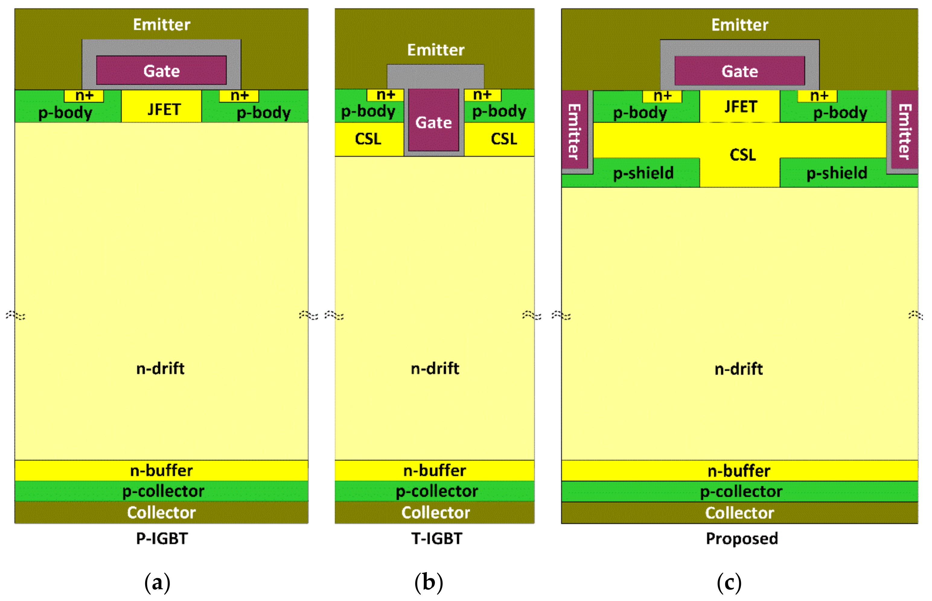
:1. Introduction
2. Device Structures and Static Characteristics
3. Dynamic Characteristics
4. Proposed Fabrication Procedure
5. Conclusions
Author Contributions
Funding
Conflicts of Interest
References
- Kimoto, T.; Cooper, J.A. Fundamentals of Silicon Carbide Technology: Growth, Characterization, Devices and Applications; Wiley: Singapore, 2014. [Google Scholar]
- Jiang, J.-Y.; Wu, T.-L.; Zhao, F.; Huang, C.-F. Numerical study of 4H-SiC UMOSFETs with split-gate and P+ shielding. Energies 2020, 13, 1122. [Google Scholar] [CrossRef] [Green Version]
- Wei, J.; Jiang, H.; Jiang, Q.; Chen, K.J. Proposal of a GaN/SiC hybrid field-effect transistor for power switching applications. IEEE Tran. Electron Devices 2016, 63, 2469–2473. [Google Scholar] [CrossRef]
- Tiwari, A.K.; Udrea, F.; Lophitis, N.; Antoniou, M. Operation of ultra-high voltage (>10kV) SiC IGBTs at elevated temperatures: Benefits & constraints. In Proceedings of the ISPSD, Shanghai, China, 19–23 May 2019; pp. 175–178. [Google Scholar]
- Cooper, J.A.; Agarwal, A. SiC power-switching devices—The second electronics revolution? Proc. IEEE 2002, 90, 956–968. [Google Scholar] [CrossRef]
- She, X.; Huang, A.Q.; Lucia, O.; Ozpineci, B. Review of silicon carbide power devices and their applications. IEEE Trans. Inductrial Electronics 2017, 64, 8193–8205. [Google Scholar] [CrossRef]
- Kadavelugu, A.; Bhattacharya, S.; Ryu, S.; Brunt, V.E.; Grider, D.; Agarwal, A.; Leslie, S. Characterization of 15 kV SiC n-IGBT and its application considerations for high power converters. In Proceedings of the ECCE, Denver, CO, USA, 15–19 September 2013; pp. 2528–2535. [Google Scholar]
- Zhang, Q.; Chang, H.; Gomez, M.; Bui, C.; Hanna, E. 10 kV trench gate IGBTs on 4H-SiC. In Proceedings of the ISPSD, Santa Barbara, CA, USA, 23–26 May 2005; pp. 303–306. [Google Scholar]
- Vechalapu, K.; Bhattacharya, S.; Van Brunt, E.; Ryu, S.; Grider, D.; Palmour, J.W. Comparative evaluation of 15-kV SiC MOSFET and 15-kV SiC IGBT for medium-voltage converter under the same dv/dt conditions. IEEE J. Emerg. Sel. Topics Power Electron. 2017, 5, 469–489. [Google Scholar] [CrossRef]
- Ryu, S.; Capell, C.; Jonas, C.; Cheng, L.; O’Loughlin, M.; Burk, A.; Agarwal, A.; Palmour, J.; Hefner, A. Ultra high voltage (>12 kV), high performance 4H-SiC IGBTs. In Proceedings of the ISPSD, Bruges, Belgium, 3–7 June 2012; pp. 257–260. [Google Scholar]
- Van Brunt, E.; Cheng, L.; O’Loughlin, M.J.; Richmond, J.; Pala, V.; Palmour, J.; Tipton, C.W.; Scozzie, C. 27 kV, 20 A 4H-SiC n-IGBTs. Mater. Sci. Forum 2015, 821–823, 847–850. [Google Scholar] [CrossRef]
- Yang, X.; Tao, Y.; Yang, T.; Huang, R.; Song, B. Fabrication of 4H-SiC n-channel IGBTs with ultra high blocking voltage. J. Semicond. 2018, 39, 34005. [Google Scholar] [CrossRef]
- Mihaila, A.; Knoll, L.; Bianda, E.; Bellini, M.; Wirths, S.; Alfieri, G.; Kranz, L.; Canales, F.; Rahimo, M. The current status and future prospects of SiC high voltage technology. In Proceedings of the IEDM Technical Digest, San Francisco, CA, USA, 1–5 December 2018; pp. 440–443. [Google Scholar]
- Linder, S. Power Electronics; EPFL Press: Lausanne, Switzerland, 2006. [Google Scholar]
- Kitagawa, M.; Omura, I.; Hasegawa, S.; Inoue, T.; Nakagawa, A. A 4500 V injection enhanced insulated gate bipolar transistor (IEGT) operating in a mode similar to a thyristor. In Proceedings of the IEDM Technical Digest, Washington, DC, USA, 5–8 December 1993; pp. 679–682. [Google Scholar]
- Mori, M.; Oyama, K.; Kohno, Y.; Sakano, J.; Uruno, J.; Ishizaka, K.; Kawase, D. A trench-gate high-conductivity IGBT (HiGT) with short-circuit capability. IEEE Trans. Electron Devices 2007, 54, 2011–2016. [Google Scholar] [CrossRef]
- Thapar, N.; Baliga, B.J. An experimental evaluation of the on-state performance of trench IGBT designs. Solid-State Electron. 1998, 42, 771–776. [Google Scholar] [CrossRef]
- Harada, S.; Kobayashi, Y.; Ariyoshi, K.; Kojima, T.; Senzaki, J.; Tanaka, Y.; Okumura, H. 3.3kV-class 4H-SiC MeV-implanted UMOSFET with reduced gate oxide field. IEEE Electron Device Lett. 2016, 3, 314–316. [Google Scholar] [CrossRef]
- Hu, S.; Huang, Y.; Liu, T.; Guo, J.; Wang, J.; Luo, J. A comparative study of a deep-trench superjunction SiC VDMOS device. J. Comput. Electron. 2019, 18, 553–560. [Google Scholar] [CrossRef]
- Sun, J.; Wei, J.; Zheng, Z.; Wang, Y.; Chen, K.J. Short circuit capability and short circuit induced VTH instability of a 1.2-kV SiC power MOSFET. IEEE J. Emerg. Sel. Topics Power Electron. 2019, 7, 1539–1546. [Google Scholar] [CrossRef]
- Uchid, K.; Hiyoshi, T.; Nishiguchi, T.; Yamamoto, H.; Matsukawa, S.; Furumai, M.; Mikamura, Y. The influence of surface pit shape on 4H-SiC MOSFETs reliability under high temperature bias tests. Mat. Sci. Forum 2016, 858, 840–843. [Google Scholar] [CrossRef]
- Li, Y.; Cooper, J.A.J.; Capano, M.A. High-voltage (3 kV) UMOSFETs in 4H-SiC. IEEE Transctions Electron Devices 2002, 49, 972–975. [Google Scholar] [CrossRef]
- Jiang, H.; Wei, J.; Dai, X.; Ke, M.; Deviny, I.; Mawby, P. SiC trench MOSFET with shielded Fin-shaped gate to reduce oxide field and switching loss. IEEE Electron Device Lett. 2016, 37, 1324–1327. [Google Scholar] [CrossRef]
- Wei, J.; Zhang, M.; Jiang, H.; Li, B.; Chen, K.J. Gate structure design of SiC trench IGBTs for injection-enhancement effect. IEEE Trans. Electron Devices 2019, 66, 3034–3039. [Google Scholar] [CrossRef]
- Wei, J.; Zhang, M.; Jiang, H.; To, S.; Kim, S.; Kim, J.; Chen, K.J. SiC trench IGBT with diode-clamped p-shield for oxide protection and enhanced conductivity modulation. In Proceedings of the ISPSD, Chicago, IL, USA, 13–17 May 2018; pp. 411–414. [Google Scholar]
- Feng, H.; Yang, W.; Onozawa, Y.; Yoshimura, T.; Tamenori, A.; Sin, J.K.O. A new fin p-body insulated gate bipolar transistor with low miller capacitance. IEEE Electron Device Lett. 2015, 36, 591–593. [Google Scholar] [CrossRef]
- Watanabe, S.; Mori, M.; Arai, T.; Ishibashi, K.; Toyoda, Y.; Oda, T.; Harada, T.; Saito, K. 1.7kV trench IGBT with deep and separate floating p-layer designed for low loss, low EMI noise, and high reliability. In Proceedings of the ISPSD, San Diego, CA, USA, 23–26 May 2011; pp. 48–51. [Google Scholar]
- Onozawa, Y.; Nakano, H.; Otsuki, M.; Yoshikawa, K.; Miyasaka, T.; Seki, Y. Development of the next generation 1200V trench-gate FSIGBT featuring lower EMI noise and lower switching loss. In Proceedings of the ISPSD, Jeju, Korea, 27–31 May 2007; pp. 13–16. [Google Scholar]
- Zerarka, M.; Austin, P.; Bafleur, M. Comparative study of sensitive volume and triggering criteria of SEB in 600 V planar and trench IGBTs. Microelectron. Reliab. 2011, 51, 1990–1994. [Google Scholar] [CrossRef]
- Li, X.; Tan, B.; Huang, A.Q.; Zhang, B.; Zhang, Y.; Deng, X.; Li, Z.; She, X.; Wang, F.; Huang, X. Impact of termination region on switching loss for SiC MOSFET. IEEE Tran. Electron Devices 2019, 66, 1026–1031. [Google Scholar] [CrossRef]
- Zhang, M.; Wei, J.; Zhou, X.; Jiang, H.; Li, B.; Chen, K.J. Simulation study of a power MOSFET with built-in channel diode for enhanced reverse recovery performance. IEEE Electron Device Lett. 2019, 1, 79–82. [Google Scholar] [CrossRef]
- Harada, S.; Kato, M.; Kojima, T.; Ariyoshi, K.; Tanaka, Y.; Okumura, H. Determination of optimum structure of 4H-SiC trench MOSFET. In Proceedings of the ISPSD, Bruges, Belgium, 3–7 June 2012; pp. 253–256. [Google Scholar]
- Sui, Y.; Tsuji, T.; Cooper, J.A., Jr. On-state characteristics of SiC power UMOSFETs on 115-um drift layers. IEEE Electron Device Lett. 2005, 26, 255–257. [Google Scholar] [CrossRef]
- Singh, R. Reliability and performance limitations in SiC power devices. Microelectron. Reliab. 2006, 46, 713–730. [Google Scholar] [CrossRef]
- Jahdi, S.; Alatise, O.; Ortiz-Gonzalez, J.; Gammon, P.; Ran, L.; Mawby, P. Investigation of parasitic turn-on in silicon IGBT and silicon carbide MOSFET devices: A technology evaluation. In Proceedings of the 2015 17th European Conference on Power Electronics and Applications, Geneva, Switzerland, 8–10 September 2015; pp. 1–8. [Google Scholar]
- Wei, J.; Zhang, M.; Jiang, H.; Wang, H.; Chen, K.J. Dynamic degradation in SiC trench MOSFET with a floating p-shield revealed with numerical simulations. IEEE Trans. Electron Devices 2017, 64, 2592–2598. [Google Scholar] [CrossRef]
- Kagawa, Y.; Fujiwara, N.; Sugawara, K.; Tanaka, R.; Fukui, Y.; Yamamoto, Y.; Miura, N.; Imaizumi, M.; Nakata, S.; Yamakawa, S. 4H-SiC trench MOSFET with bottom oxide protection. Mater. Sci. Forum 2014, 778–780, 919–922. [Google Scholar] [CrossRef]
- Wei, J.; Xie, R.; Xu, H.; Wang, H.; Wang, Y.; Hua, M.; Zhong, K.; Tang, G.; Zhang, M.; Chen, K.J. Charge storage mechanism of drain induced dynamic threshold voltage shift in p-GaN gate HEMTs. IEEE Electron Device Lett. 2019, 40, 526–529. [Google Scholar] [CrossRef]
- Oyama, K.; Kohno, Y.; Sakano, J.; Uruno, J.; Ishizaka, K.; Kawase, D.; Mori, M. Novel 600-V trench high-conductivity IGBT (trench HiGT) with short-circuit capability. In Proceedings of the ISPSD, Osaka, Japan, 7 June 2001; pp. 417–420. [Google Scholar]
- Antoniou, M.; Lophitis, N.; Bauer, F.; Nistor, I.; Bellini, M.; Rahimo, M.; Amaratunga, G.; Udrea, F. Novel approach toward plasma enhancement in trench-insulated gate bipolar transistors. IEEE Electron Device Lett. 2015, 36, 823–825. [Google Scholar] [CrossRef]
- Yonezawa, Y.; Mizushima, T.; Takenaka, K.; Fujisawa, H.; Deguchi, T.; Kato, T.; Harada, S.; Tanaka, Y.; Okamoto, D.; Sometani, M.; et al. Device performance and switching characteristics of 16 kV ultrahigh-voltage SiC flip-type n-channel IE-IGBTs. Mater. Sci. Forum 2015, 821–823, 842–846. [Google Scholar] [CrossRef]
- Mikamura, Y.; Hiratsuka, K.; Tsuno, T.; Michikoshi, H.; Tanaka, S.; Masuda, T.; Wada, K.; Horii, T.; Genba, J.; Hiyoshi, T.; et al. Novel designed SiC devices for high power and high efficiency systems. IEEE Trans. Electron Devices. 2015, 62, 382–389. [Google Scholar] [CrossRef]
- Ghandi, R.; Bolotnikov, A.; Lilienfeld, D.; Kennerly, S.; Ravisekhar, R. 3kV SiC charge-balanced diodes breaking unipolar limit. In Proceedings of the ISPSD, Shanghai, China, 19–23 May 2019; pp. 179–182. [Google Scholar]


| Parameter | Value | Unit |
|---|---|---|
| Doping of n-drift | 2.5 × 10¹⁴ | cm−3 |
| Thickness of n-drift | 180 | µm |
| Gate oxide thickness | 50 | nm |
| Channel mobility | 30 | cm2/V-s |
| Channel length | 1 | µm |
| Doping of JFET | 2 × 10¹⁶ | cm−3 |
| Doping of p-shield | 1 × 10¹⁸ | cm−3 |
| Thickness of p-shield | 1 | µm |
| Doping of CSL | 2 × 10¹⁶ | cm−3 |
Publisher’s Note: MDPI stays neutral with regard to jurisdictional claims in published maps and institutional affiliations. |
© 2020 by the authors. Licensee MDPI, Basel, Switzerland. This article is an open access article distributed under the terms and conditions of the Creative Commons Attribution (CC BY) license (http://creativecommons.org/licenses/by/4.0/).
Share and Cite
Zhang, M.; Li, B.; Zheng, Z.; Tang, X.; Wei, J. A New SiC Planar-Gate IGBT for Injection Enhancement Effect and Low Oxide Field. Energies 2021, 14, 82. https://doi.org/10.3390/en14010082
Zhang M, Li B, Zheng Z, Tang X, Wei J. A New SiC Planar-Gate IGBT for Injection Enhancement Effect and Low Oxide Field. Energies. 2021; 14(1):82. https://doi.org/10.3390/en14010082
Chicago/Turabian StyleZhang, Meng, Baikui Li, Zheyang Zheng, Xi Tang, and Jin Wei. 2021. "A New SiC Planar-Gate IGBT for Injection Enhancement Effect and Low Oxide Field" Energies 14, no. 1: 82. https://doi.org/10.3390/en14010082