Article

A New GaN-Based Device, P-Cascode GaN HEMT, and Its Synchronous Buck Converter Circuit Realization

1
Mechanical and Mechatronics Systems Research Laboratories, Industrial Technology Research Institute, Hsinchu 31040, Taiwan
2
Department of Mechanical Engineering, College of Engineering, National Chiao Tung University, Hsinchu 30010, Taiwan
3
Department of Material Science and Engineering, National Chiao Tung University, Hsinchu 30010, Taiwan
*
Author to whom correspondence should be addressed.
Energies 2021, 14(12), 3477; https://doi.org/10.3390/en14123477
Submission received: 19 May 2021 / Revised: 9 June 2021 / Accepted: 10 June 2021 / Published: 11 June 2021
(This article belongs to the Special Issue Wide Bandgap Technologies for Power Electronics)

Abstract

:
This paper attempts to disclose a new GaN-based device, called the P-Cascode GaN HEMT, which uses only a single gate driver to control both the D-mode GaN and PMOS transistors. The merit of this synchronous buck converter is that it can reduce the circuit complexity of the synchronous buck converter, which is widely used to provide non-isolated power for low-voltage and high-current supply to system chips; therefore, the power conversion efficiency of the converter can be improved. In addition, the high side switch using a single D-mode GaN HEMT, which has no body diode, can prevent the bi-directional flow and thus reduce the power loss and cost compared to a design based on a series of two opposite MOSFETs. The experiment shows that the proposed P-Cascode GaN HEMT efficiency is above 98% when it operates at 500 kHz with 6 W output. With the input voltage at 12 V, the synchronous buck converter provides an adjustable regulated output voltage from 1.2 V to 10 V while delivering a maximum output current of 2 A.

1. Introduction

Synchronous buck converters are widely used in industries, consumer, and automotive applications. As the size becomes more compact, designers have turned to faster switching speeds in order to reduce the size of the converter [1,2]. However, the switching speed is limited by the switching loss and the reverse recovery characteristic of the transistors. Therefore, wide-bandgap devices, such as GaN and SiC, have the potential benefits of achieving high switching and high efficiency capability because of their superior material properties, including a small gate charge and low Coss loss [3,4]. The disadvantage of the GaN HEMTs is the normally-on characteristic with negative Vth. From the fail-safe and simple gate drive point of view, cascode configuration is one of the suitable ways to turn the normally-on into normally-off devices [5].
Few studies have presented the benefits of the cascode configuration to achieve the advantages of a high switching operation, high efficiency performance, and simple gate drive circuit requirement [6,7]. A cascode SJ-FET/LV-FET configuration, which avoids the activation of the body diode by keeping the SJ-FET in the on-state, provides better performance in the third quadrant operation [6]. In [7,8], demonstration of the cascode GaN/SiC power device, combining the benefits of a GaN device’s fast switching ability and a SiC device’s high-voltage blocking capability, was shown to reach lower Coss loss and higher device ratings. Nevertheless, the aforementioned literature results show great performance in cascode configuration with respect to in the standalone configuration, the issues being the match in intrinsic capacitances [9], an avalanche in the low side switch [10], and stray inductance analysis between the two cascode devices’ interconnection [11,12]. Decayed Negative Voltage [13] and dv/dt control [14] were proposed to solve the switching controllability, suppress the oscillation, and prevent the false turn-on phenomenon. Cascode configuration provides a positive Vth to control the GaN HEMT, but it is still limited by the package parasitic capacitance [15]. There is big appreciation of the development teams of previous work on NCTU GaN HEMT devices, covering every aspect of materials, process development, devices [16,17,18], thermal performance [19,20], and the spice model [21,22], leading to the lab-made cascode GaN HEMT, equipped to potentially be capable of being realized in circuit applications. However, the cascode topology faces two problems which includes the switching frequency limited by the NMOS switch, and the returning current flow from the load to the power source due to the body diode of the high-side E-mode transistor, which makes it unsuitable for synchronous rectifier applications. Therefore, a P-Cascode GaN HEMT Module topology is proposed. The GaN HEMT in this paper is used as the high side switch that can go to several MHz, switching with a very small switching loss due to its output capacitance. Coss varies much less than the MOSFET and the energy loss in the reverse recovery charge process is insignificant with respect to the MOSFET.
The novel P-Cascode GaN device is implemented by using discrete TO-220 package D-mode MIS-HEMT GaN and TO-220 package P-MOSFET. Comparing to the previous achievements in NCTU [16,17,18,19,20,21,22], which needed two E-mode cascode GaN HEMT devices to achieve the synchronous bulk operations, we need only one P-Cascode GaN device to implement the same operations. The aim of this paper is to reduce the shooting through problems inherent in the synchronous buck converter. Previous achievements will need two individual gate drivers, which follow the well-known dead-time control to prevent the shooting through. The novelty of this work is to use a single P-Cascode GaN power module that embodies only one gate drive to yield the equivalent dead-time control for preventing the shooting-through problem. The efficiency can be improved due to the number of devices used being cut in half.
This paper introduces the P-Cascode GaN power module in the following order. This paper is organized as follows. The novel P-GaN cascode device is presented by using a discrete TO-220 package D-mode MIS-HEMT GaN and TO-220 package P-MOSFET. To fulfill the transistor-matching issues, the characteristics of the D-mode MIS-HEMT GaN is studied, including the epitaxial structure and the field plate, in Section 2.1, to provide the designed information for circuit configuration. Section 2.2 reviews the previous lab-made GaN HEMTs cascode topology from NCTU [16,17,18,19,20,21,22]. Due to this cascode topology, which did not perform well in synchronous rectifier applications for solving the switching frequency limited by the NMOS switch and the returning current flow from the load problems, a single gate controlled P-Cascode GaN HEMT module configuration is proposed in Section 2.3. To provide the compatible gate drive for the proposed single gate P-Cascode GaN HEMT, the biased charge pump gate drive is presented in Section 2.4. Then, the synchronous buck converter based on the created P-Cascode GaN HEMT module with the biased charge pump gate drive is analyzed and used to verify the performance in Section 2.5. The experimental results and conclusion are shown in Section 3 and Section 4.

2. Materials and Methods

2.1. D-Mode GaN MIS-HEMT Characteristics

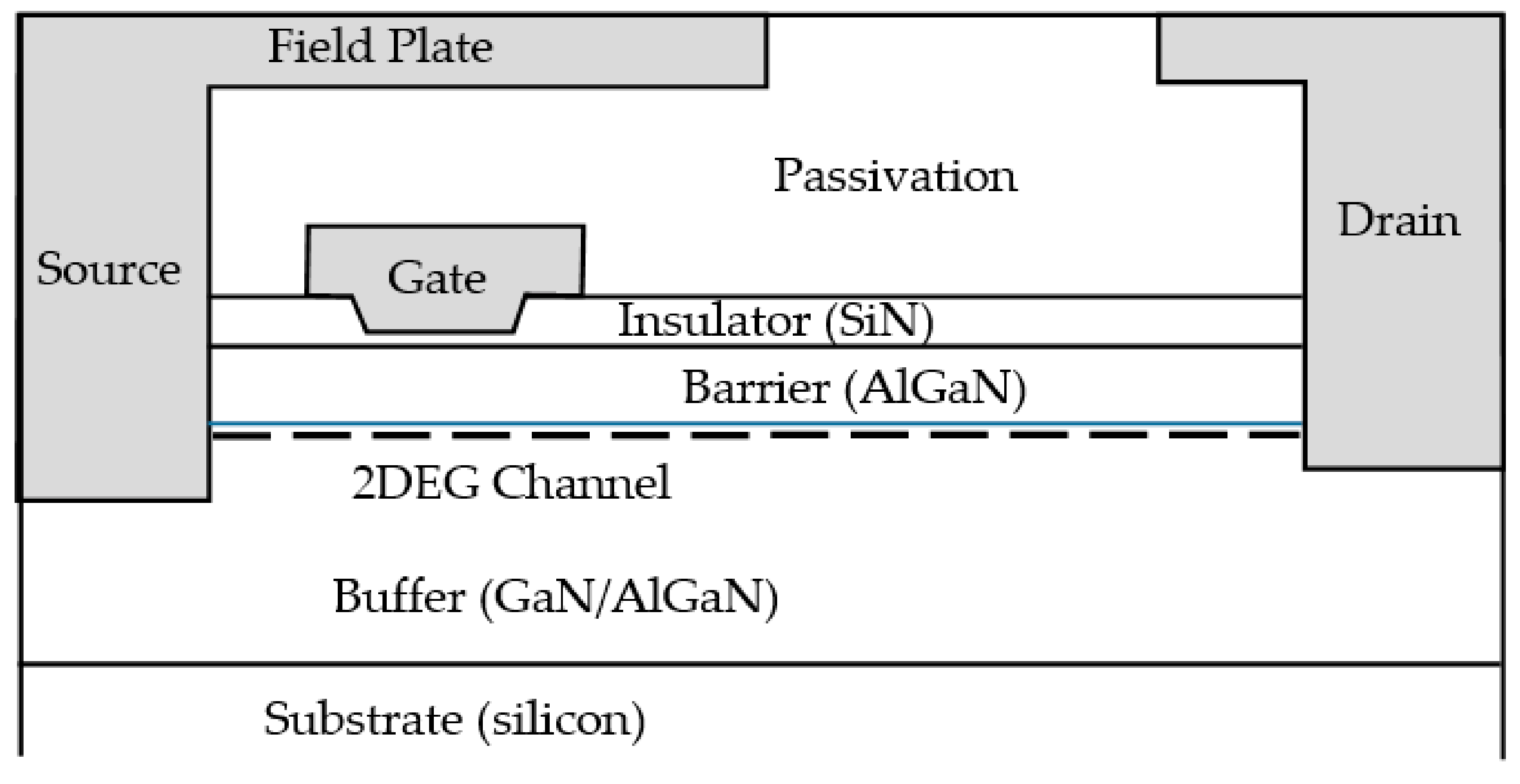
From the top to the bottom, the epitaxial structure of our GaN device consists of a 2 nm SiNx and 1 nm GaN cap, a 25 nm AlGaN barrier layer, a 1 um GaN layer, a 4 um-thick AlGaN/AlN supper-lattice buffer layer, an AlN seed layer, and the Si substrate; the schematic cross section of the epitaxy structure is shown in Figure 1a. The 120 mm GaN MIS-HEMT process can be divided into four parts (Process flow and 120 mm GaN MIS-HEMT design and pictures shown in Figure 1b), including the ohmic contact, mesa isolation, gate formation, and field-plate formation. The fabrication process of the ohmic contact and mesa isolation is presented in [23]. A 40 nm SiNx passivation layer was deposited by plasma-enhanced chemical vapor deposition (PECVD). For device gate formation, a two-step gate was defined by the mask aligner using the photoresist T-gate structure, a field plate defined by the mask aligner, and metal deposition of the Ti/Au by e-gun. Finally, a 100 nm SiNx layer was deposited with nitride via the fabricated device pad region. After device fabrication, the Si substrate back side grinding, polishing, and back side metal deposition were formatted, and after chip dicing, all the GaN devices were packaged in a TO220 case package.
The parasitic capacitance CISS = CGD + CGS is only 6% [24] smaller when the transistor is turning on than when turning off. Hence, the turn-on delay time will be similar to the turn-off delay time. The electrode of the field plate, as shown in Figure 2, represents a metallization above the passivation layer, making the GaN HEMT possible to reach exceptional power densities. That allows modifying some electric properties of the HEMT, such as the distribution of the electric field at the edge of the gate near the drain and the breakdown voltage. One dominant effect of the field plate is that the distribution of the electric field at the edge of the drain and gate side reduces the peak of the electric field. However, it also equalizes the roles of the source and the drain and made them undistinguishable.
In order to evaluate the effect of field plate, the switching test as shown in Figure 3 is proposed. In the switching test, each terminal of the drain and source is connected to a 10 Ω resistor. The VDD = 12 V is used to float the source to 6 V while the gate voltage is applied with a low frequency, 10 Hz, triangular wave input. The D-mode GaN MIS-HEMT is gradually turned on from VG = −10 V to 10 V. For the switching test (I), when the gate is turning on, there is an increasing feedback voltage on the source terminal to reduce the gate-source voltage, which is equivalent to the Miller plateau effect that the current iD can only increase slowly. As shown in Figure 4, the function of vGD in terms of vGS is proposed to observe the voltage feedback effect from the resistors. The switching test is used to justify the degree of drain-source symmetry of the transistor as follows.
In Switching Test (I), we have
vGS = vG − 10iD
vGD = vG + 10iDVDD
that yields
vGDvGS = 20iDVDD
In Switching Test (II), we have
vGSvGD = 20iDVDD
Since the gate voltage vG, a triangular wave input, is implicit in both Equations (3) and (4), the voltage feedback 20iD from the resistors can help to show the turn-on and turn-off transitions as well as to indicate the threshold voltages, as shown in Figure 4. In the turn-on states, both switching tests yield vGDvGS due to the drain-source voltage vDS being small. In the turn-off states, the Switching Tests (I) is vGDvGS = VDD and (II) is vGDvGS = −VDD due to iD being zero.
On the other hand, when the gate is turning off, the decreasing feedback voltage will increase the gate-source voltage, which causes the current iD to decrease slowly. In case that the drain and source terminals are perfectly symmetric to the gate on the D-mode GaN MIS-HEMT, Switching Test (II) will be symmetric to Switching Test (I) with respect to the vGD = vGS axis.
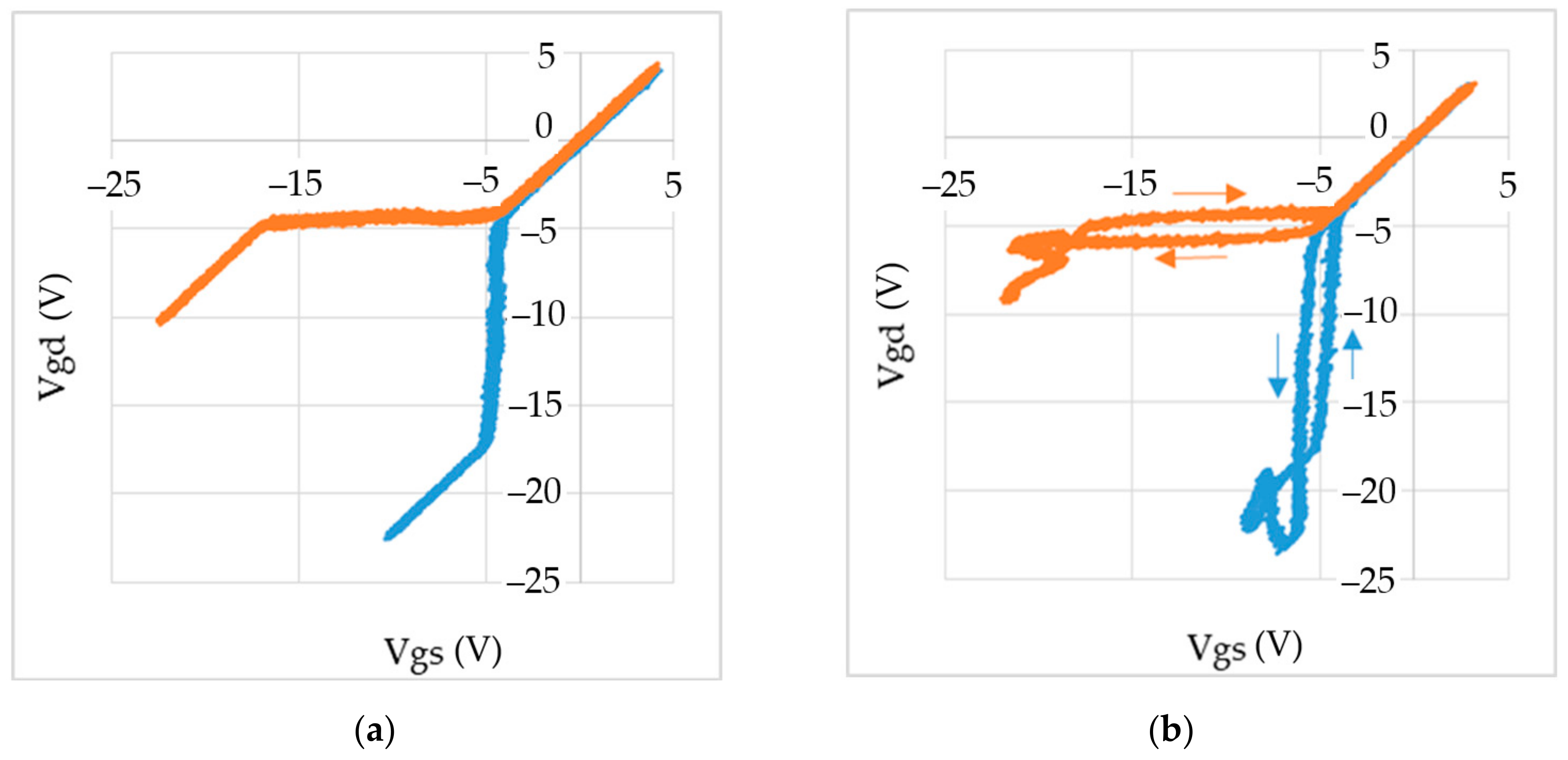
The experimental result is shown in Figure 5. According to the experiment’s result, the gate-source voltage determines that turn-on and turn-off is a function of switching frequency. In the frequency lower than 1 kHz, the turn-on and turn-off voltage of the D-mode GaN is identical, which are both −4 V. In a high frequency higher than 100 kHz, the turn-on and turn-off voltage of the D-mode GaN become different from each other. The experiments show that the traces of the turn-on process remain the same as the low frequency one and the turn-on voltage is −4 V, i.e., VTg(on) = 4 V. On the other hand, the turn-off voltage yields a different trace and the turn-off voltage is −7 V, i.e., VTg(off) = 7 V. The experiment also shows that the reverse recovery charge process during the turn-off time causes an overshoot voltage on vDS. As a matter of fact, Switching Test (II) will be symmetric to Switching Test (I) with respect to the vGD = vGS axis; therefore, the drain and source terminals are perfectly symmetric to the gate on the D-mode GaN MIS-HEMT. In summary, the characteristics of the GaN HEMT and TO220 packaging are displayed in Table 1. The stray inductance of the TO220 packaging measured from the RLC meter GWINSTEK LCR819 at the drain (high) to source (low) and the source (low) to drain (high) is around 100 nH.

2.2. Cascode GaN HEMT Module as an E-Mode Switch

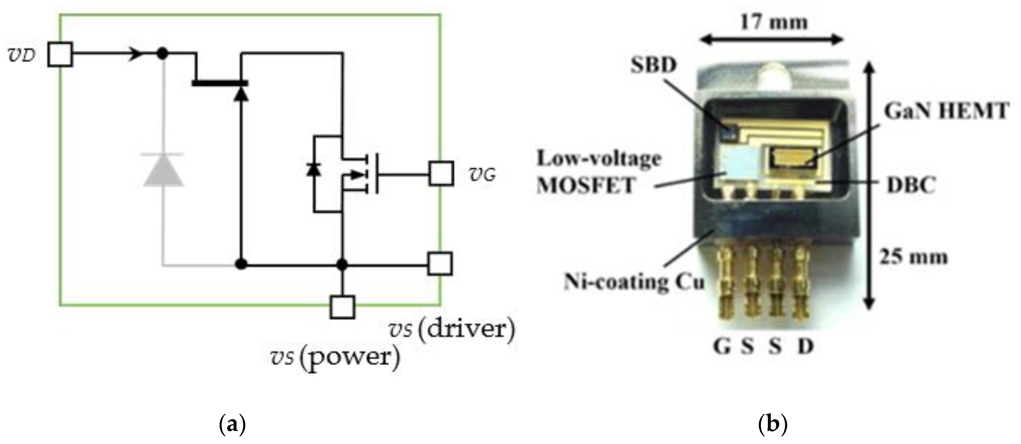
A cascode configuration that comprises a high-voltage, normally-on GaN HEMTs device and a low-voltage silicon NMOS is shown in Figure 6 [16,17,18,19,20,21,22].
AlGaN/GaN HEMTs function in the depletion mode, limiting their range of applications. Normally-off operation is required in industrial power drive circuits to satisfy the fail-safe criteria and provide a simple gate drive configuration. A popular means of satisfying the normally-off requirement is to use a cascode configuration that comprises a high-voltage, normally-on GaN HEMTs device and a low-voltage silicon NMOS, as shown in Figure 6. In order to control the ON/OFF state of the normally-on GaN switch behaving as a normally-off device that is compatible with the commercial gate driver, a cascoding 80 mm D-mode GaN device, SiC SBD, and a low-voltage NMOS was achieved in NCTU [16,17,18,19,20,21,22].
The cascode GaN HEMT is using the NMOS as a switch to turn on and off the power path from drain to source when vDS is forward biased. When vDS is reverse biased, the gate-source voltage of the D-mode GaN is vSD according to the result from Figure 5, where the power path from the NMOS body diode to the D-mode GaN is naturally on. Therefore, the SiC SBD is unnecessary in the power module. The cascode GaN HEMT power module worked as an E-mode transistor that can endure a high breakdown voltage; however, the switching frequency is limited by the NMOS switch. In a particular application, such as a synchronous buck converter such as the MTK pump express®, the body diode of the high side E-mode transistor is not preferred because of the returning current flow from the load to the power source is prevented. Thus, it was practical to use two E-mode transistors side by side. Reverting the drain and source of one transistor eliminates the body diode effect. However, it imposes an extra cost on the buck converter fabrication.

2.3. P-Cascode GaN HEMT Module as a Double Throw Switch

In contrast with the cascode GaN HEMT, the P-Cascode GaN HEMT, as shown in Figure 7, with a cascoding 200 mm D-mode GaN HEMT device and a low-voltage P-MOS, is proposed in this paper. The P-Cascode GaN HEMT employs four terminals, including the source (S), drain (D), gate (G), and the output (O), in which vOG is the source-gate voltage of the PMOS, vOS is the source-drain voltage of the PMOS, vGD is the gate-source voltage of the GaN HEMT, and vOD is drain-source voltage of the GaN HEMT.
We have performed the same on–off experiment according to Figure 3. The result shows that the threshold voltage VTp of the PMOS turn-off is slightly higher than that of the turn-on. There is no significant bifurcation between turn-on and turn-off. The turn-off threshold voltage denoted by VTp(off) is 4.0 V and the turn-on threshold voltage denoted by VTp(on) is 3.8 V (Figure 8).
In the operation of vDO > 0, the characteristics of the module in the linear ohmic region may be simplified as follows.
id = KGaN((vGD + VTg) vDOvDO2/2) = vDO/ron,GaN if min(vGD, vGO) > −VTg,
id = 0    else
The on-resistance of GaN HEMT denoted by ron,GaN is a function of both (vGD + VTg) and vDO. In general, the resistance ron,GaN is also a function of the junction temperature of the GaN HEMT in the module. In this study, the GaN HEMT is a depletion mode device implying −VTg < 0. On the other hand, the characteristics of PMOS yields that
i2 = KPMOS((vOGVTp) vOSvOS2/2) = vOS/ron,PMOS if vOG > VTp,
i2 = 0    else
The on-resistance of PMOS denoted by ron,PMOS is a function of both (vOGVTp) and vOG. Let vO be toggled between two states vOH and vOL, which corresponds to the output voltage when the GaN HEMT and PMOS is turned on, respectively. The transistors GaN HEMT and PMOS shall be turned alternatively. To prevent the situation of both switches being simultaneously turned on is known as “shooting through”. The situation where both transistors are turned on will cause the shooting through from the voltage source connected to vD to the ground connected to vS. Thus, the output voltage may be shown as follows.
vO = VOH = vDid ron,GaN  if min(vGD, vGO) > −VTg,
vO = VOL = vSi2 ron,PMOS    if vOG > VTp
In a particular application, such as the synchronous buck converter, we have vD = VDD and vs. = 0 V. Since GaN HEMT and PMOS are turned on alternatively, id = i2 = io > 0. The output voltage may be expressed as follows.
VOH = VDDio ron,GaN  if min(vGD, vGO) > −VTg,
VOL = −io ron,PMOS     else
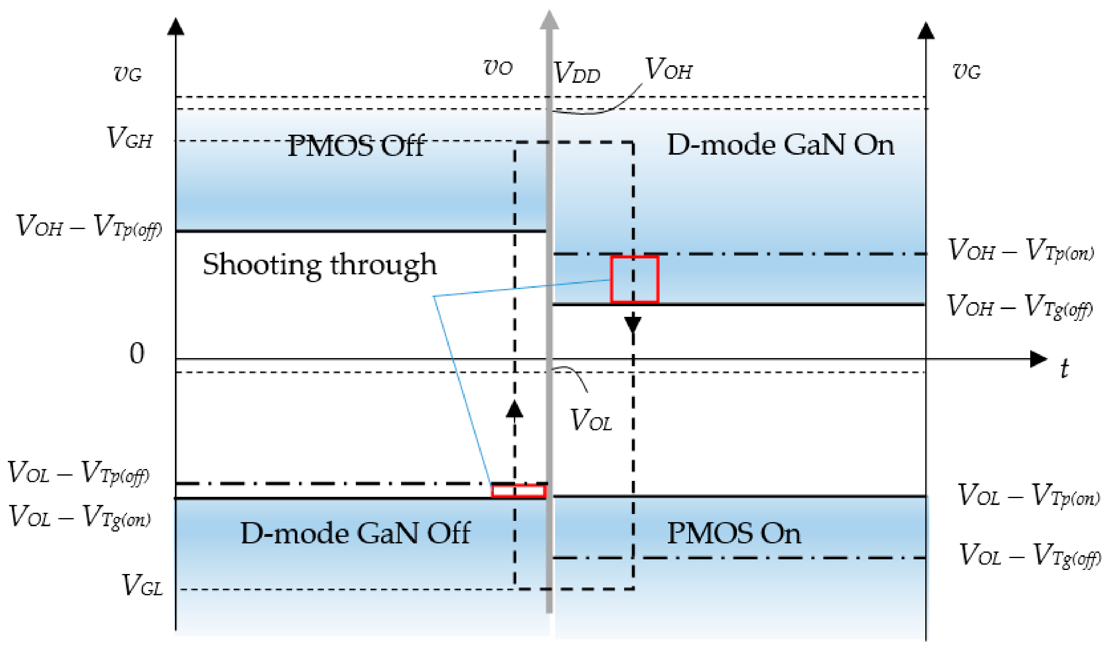
The gate must be rapidly changed in order to make only one transistor on at a time. The required gate voltage to turn off the PMOS is VGHVOHVTp. The gate voltage to turn off the GaN is VGLVOLVTg. The swing of the gate voltage is
VGG = VG,swing = VGHVGLVOHVOLVTp + VTg,
In a practical case of VOH~VDD and VOL~0, if we select VTg = VTp, then the minimum gate swing VGGVDD is seen. In case of VTg(off) > VTp(on), as shown in Figure 9, when the gate driver turns on to VGH and turns off to VGL cyclically, there will be time periods that both the GaN HEMT and PMOS are simultaneously turned on. This shooting through problem becomes more serious when at a higher frequency switching, where VTg(off) increases, as referred to in the result in Table 1. To prevent this shooting through problem, it is recommended to choose a PMOS whose VTp(on) > VTg(off) and also VTp(off) > VTg(on).
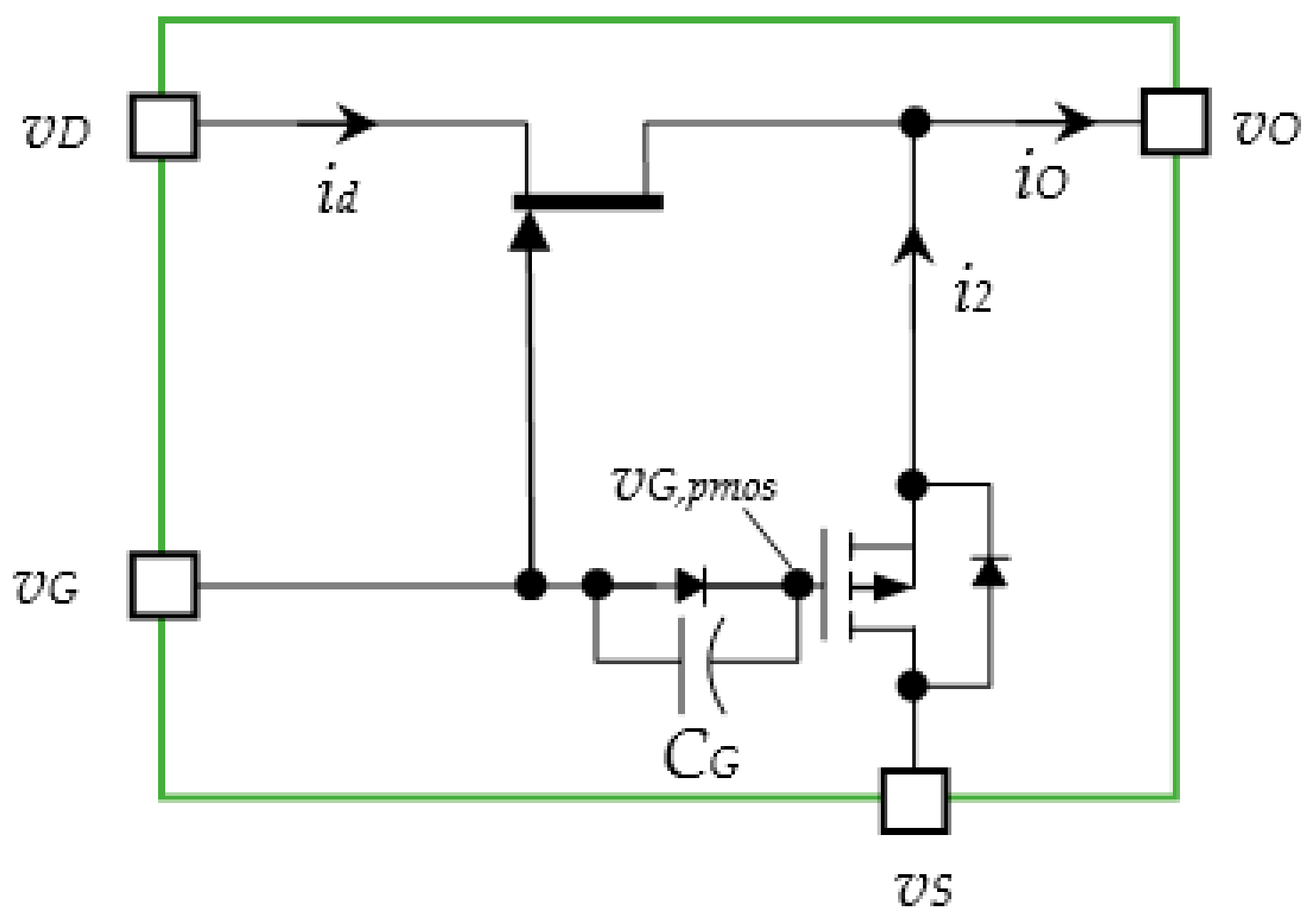
In case that a PMOS failed to fulfill only the condition that VTp(on) > VTg(off), we can add a capacitor in front of the gate of the PMOS, as shown in Figure 10. In such an arrangement, the gate signal can fulfill these two requirements.
The ratio ρ < 1 is a function that
VG,pmos(t) = vG(t) if vG > 0
VG,pmos(t) = ρvG(t) else (ρ = CGS/(CG + CGS))
It shall note that vG,pmos(t) is in synchronous with vG(t), hence the circuit shown in Figure 10 is proposed to prevent the shooting through problem during only vG < 0. In Figure 10, we added a single direction capacitor CG in front of the gate of the PMOS. The single direction capacitor is used as a voltage divider to take only a part of the gate voltage vG into the gate in the PMOS; the voltage relation is as follows.
vG,pmos(t) = [CGS/(CG + CGS)] vG
One other phenomenon that can occur is the gate voltage vg is also bonded by VGLvGVOH and the voltage vO is bounded by VOLvOVOH, when GaN HEMT is turning off at time t:
vG = VGH(1 − t) + VGL t
The output voltage vO after a time delay tD will follow the gate signal to go to a low voltage VOL:
vO = vOH(1 − γt) + vOL ∙γt, when t > tD
This time delay is known as the recovery charge process plus the time required for vG to fall below VOHVTg, as shown in Figure 11. After time tD when vG falls, the output voltage vO falls simultaneously. It may occur when vO rushes down to VOL faster than vG falls to VGL so that vG < voVTg and the GaN HEMT turns off again, which will cause the output ringing. To prevent this, we need to reduce the gate resistance and, equivalently, to increase γ in Equation (13).

2.4. Biased Charge-Pump Gate Drive Design

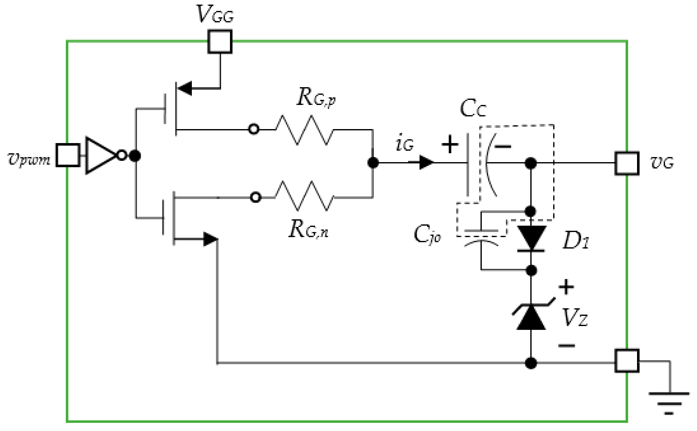
The kind of charge-pump gate drive presented by Ishibashi [25] for the D-mode devices is useful for driving the D-mode GaN MIS-HEMT. The biased charge-pump circuit in Figure 12 uses CC to shift the gate voltage level. To reduce ringing, resistors RG,p and RG,n in series with the capacitor are used to slow down the turn-on of the GaN HEMT and turn-on of the PMOS.
The charge-pump circuit in Figure 12 uses CC to lower the gate supply below the supply voltage of the gate power stage. Resistors RG,p and RG,n in series with the capacitor can reduce ringing by slowing down the turn-on of the GaN HEMT and turn-on of the PMOS. The slower turn-on allows more time for the parasitic network to discharge, limiting the ringing. The value of the boot resistor is determined empirically; starting at 0 Ω, and then increasing the resistance until the ringing is reduced to the desired level. Ideally, the charge-pump gate drive converts the output of VGG to a 0 V gate signal into a 0 to −VGG gate signal. The swing of the gate drive signal remains VG before and after the capacitor and a diode is added toward the normal gate drive circuit. In order to further shift the signal to above 0 V, a Zener diode with the reverse breakdown voltage VZ is used to clamp the gate signal. The output of the gate drive in the steady state is
vG = vGH = VZ if vpwm = 5 V
vG = vGL = VZVGG if vpwm = 0 V
As mentioned in the previous section, vGHVDDVTp and vGLVTg, and the choice for the VZ is as follows.
VTg + VGGVZVDDVTp
When we have a close look at the equivalent circuit of a p-n junction diode, two types of capacitance take place: transition capacitance (CT) and the diffusion capacitance (CD).
Cjo = CT + CD
In a forward biased diode, diffusion capacitance is much larger than the transition capacitance. Hence, diffusion capacitance is considered in forward-biased diodes. When the gate drive vpwm is high, the current iG goes through VGG to the ground. The current iG goes through the ground back to the ground when vs is low. In Figure 12, we first assume that RG,p = RG,n = RG. In the steady state when the gate signal vpwm is high, the diode D1 is in the forward bias, the charge on the diode D1 is
QG,h1 = CD (vG,hVZ)
The charge on the capacitor’s CC side is
QG,h2 = CC (VGGvG,h)
If the charge conservation law is applicable in the dotted box shown in Figure 9 during the time when the gate signal vpwm is low, the diode D1 is in the reverse bias, and the charge on the diode’s D1 side is
QG,h1 +ΔQ = CT (vG,lVZ)
The charge on the capacitor’s CC side is
QG,h2 + ΔQ = CC (0 − vG,l)
It is obtained that
(CD + CC)vG,h − (CC + CT)vG,l = CCVGG + (CDCT)VZ
In case that CC >> CD >> CT and the diode drains out of the charges during the reverse bias session, so that QG,h1 + ΔQ ≅ 0, then
vG,hvG,l = VGG
vG,l = VZ
The Zener diode is then used instead of a DC battery to lift the charge pump output voltage by an amount of the Zener diode’s breakdown voltage.

2.5. Synchronous Buck Converter

Buck converters can be highly efficient (often higher than 90%), making them useful for tasks such as converting a computer’s main (buck) supply voltage (often 12 V) down to lower voltages needed by USB (5 V) and DRAM or (1.8 V or 1.25 V or less) using a high-side (HS) MOSFET switch with an adjustable duty. A synchronous buck converter is a modified version of the basic buck converter circuit topology in which the flyback diode is replaced by a low-side (LS) switch, typically another MOSFET switch. Conventional buck converters will delay the turn-on and bring forward the turn-off time to overcome the shooting-through problem; however, it will require two gate drives and a microprocessor to maintain the delay time tD (Figure 13). The sorting according to the gate drive IC and MOSFET is required to improve the reliability of the synchronous buck converter products. There are gate-driving techniques other than dead-time control, including the zero voltage switching (ZVS) or the zero current control (ZCS), which are useful in high-voltage applications such as the flyback converter [26] and class-E amplifier [27]. For the low input voltage applications, such as the buck converter, the ZVS or ZCS is useful in the discontinuous current mode (DCM), which supplies only low power output. In the context of this paper, we focused only on the continuous current mode (CCM) application using the synchronous buck converter for maintaining the stable voltage output.
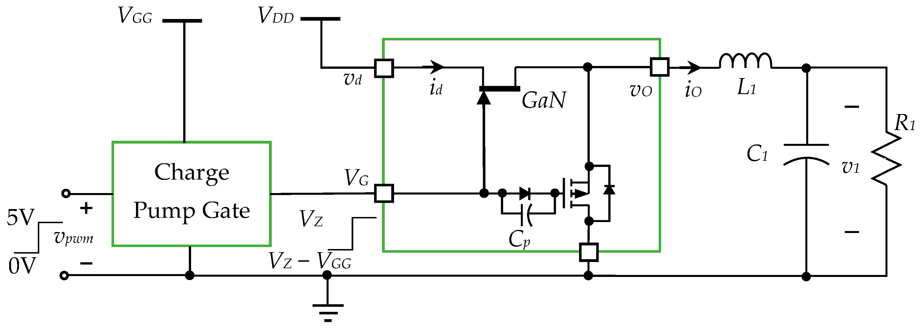
The proposed buck converter, as shown in Figure 14, consists of a P-Cascode GaN HEMT switch module, the body diode of the PMOS, output inductor L1, and output capacitor C, within which only a single gate drive is needed to control both transistors. Features of the proposed synchronous buck converter include (a) it can simplify the gate drive control for only a single gate used; (b) it has no need for two opposite MOSFETs to block the bi-directional current flow on the high side as the GaN HEMT has no body diode (or flyback diode); and (c) the P-Cascode GaN HEMT can be packaged as a whole, reducing the stray inductance and parasitic capacitance. A GaN HEMT with no body diode makes it suitable for half-bridge hard switching, which means no additional hard commutation due to zero reverse recovery. This makes the EMI design simpler and boosts performance. It is especially helpful in compact designs where power conversion and signal processing are on the same small PCB.
The GaN HEMT switches between the on and off states during operation. When GaN HEMT is on, the input voltage is connected to the load through the inductor. The capacitor is charging, and the output voltage begins to rise toward the input voltage. The body diode of the PMOS is reverse-biased.
During operation, the GaN HEMT alters between the closed (on) and open (off) states. When GaN HEMT is closed, the input voltage is connected to the load through the inductor, which stores energy in its magnetic field. The capacitor is charging, and the output voltage begins to rise toward the input voltage. The body diode of the PMOS is reverse-biased. The synchronous buck converter improves efficiency by substituting the PMOS switch for the body diode conduction. When a PMOS is used for the lower switch, some diode losses may occur during the time between the turn-off of the high-side GaN and the turn-on of the low-side PMOS, when the body diode of the low-side PMOS conducts the output current.
When GaN HEMT turns on in the duty δ of a period time TS, the inductor current io rises from io,min, to
io,max = (VDDV1Ioron,GaN) δTS/L1 + io,min
Io denotes the average current of io. When GaN HEMT turns off, the inductor current io falls from io,max
io,min = (−Ioron,PMOSV1) (1 − δ)TS/L1 + io,max
Comparing to Equation (25) with (26), we have
V1 = δVDDIo (δ(ron,GaNron,PMOS) + ron,PMOS)
By selecting properly ron,GaNron,PMOS, the above equation yields that
V1 = δVDDIo ron,PMOS
Equation (25) yields that
io,max = δ(1 − δ)VDDTS/L1 + io,min
The energy stored in the magnetization inductor L1 is sent to the resistor during the turn-off time, which is
(1/2)L1(io,max2io,min2) = (1 − δ)TS(V12/R1) ≈ (1 − δ)TSδVDD (δVDD − 2Io ron,PMOS)/R1
From Equations (25) and (29), we obtain that
((1 − δ) VDDδTS/L1 + io,min)2io,min2 = 2(1 − δ) δVDDTS(δVDD − 2Io ron,PMOS)/L1R1
When io,min >> (1 − δ) VDDδTS/L1, the above equation can be simplified into
io,min = (δVDD − 2Io ron,PMOS)/R1
The average output current Io is
Io = (io,maxio,min)/2 = δ(1 − δ)VDDTS/2L1 + (δVDD − 2Io ron,PMOS)/R1
The above equation can be simplified into
Io = δVDD (1 + (1 − δ) R1TS/2L1)/(R1 (1 + 2ron,PMOS/R1))
In applications where ron,PMOS/R1 << 1, the above equation is simplified into the following by defining β = R1TS/2L1.
Io = δVDD (1 + β(1 − δ))/R1
In terms of the switching frequency, the time factor β may be written as
β = R1/2L1fs
The power loss on the transistors consists of two parts: (1) the on-resistance loss; and (2) the switching loss of the GaN HEMT. Again, assuming that ron,GaNron,PMOS, the total power loss
PLoss = PL,on + PL,switching = (δIo2ron,GaN + (1 − δ) Io2ron,PMOS) + αIoVDD = Io(Ioron + αVDD)
Comparing with the total power input, we obtain the conversion efficiency η as follows.
η = (1 − PLoss/Pin) × 100% = ((1 − α/δ) − Ioron/VDD) × 100%
In practice, ron is a monotonic increasing function of Io and Io is a monotonic increasing function of the duty ratio. The switching loss factor α is dependent on duty δ. Equation (37) implies that the switching loss at a low duty ratio and the on-resistance loss at the high duty ratio are the dominant factor of the conversion efficiency. Furthermore, the higher VDD means the switching loss becomes more dominant in the conversion efficiency.
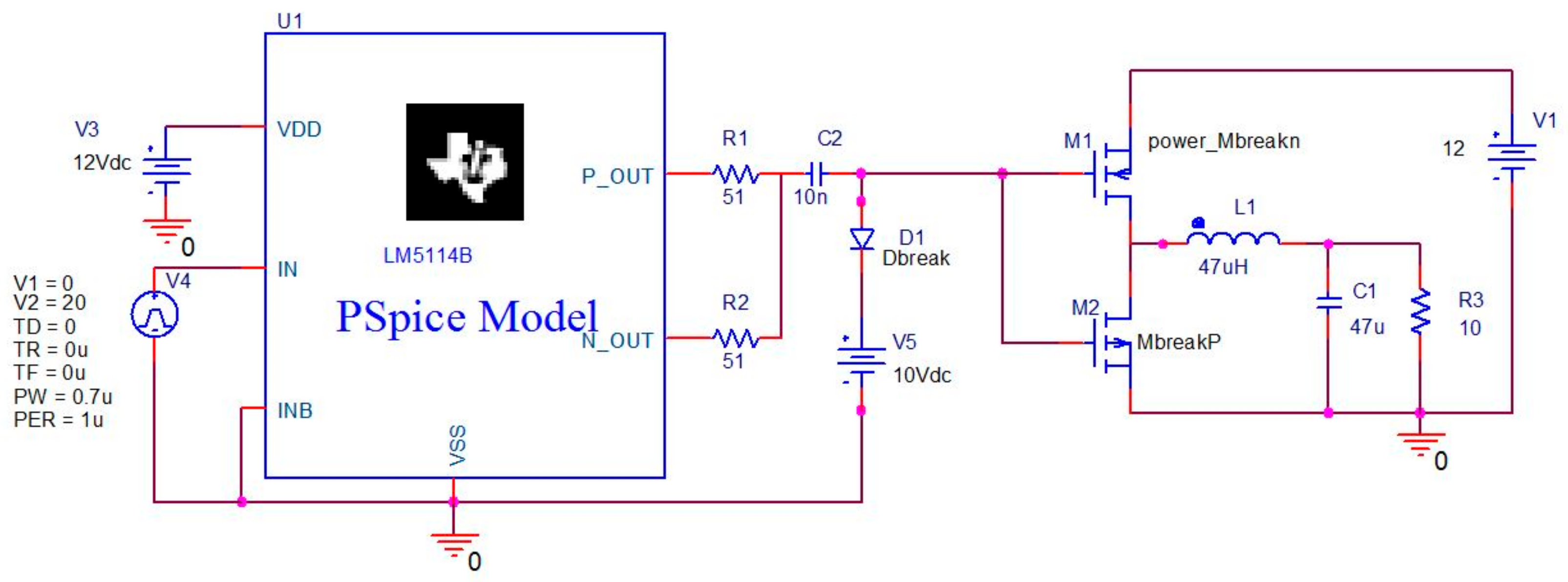
The ORCAD PSPICE simulation model for the synchronous buck converter is shown in Figure 15. Instead of using a Zener diode, a DC voltage with 10 V to present the reverse break down voltage of the Zener diode is used. The D-mode GaN HEMT is also replaced by a Power NMOS whose VTO is set to be −4 V to simulate the D-mode GaN HEMT. The gate drive is also simplified by directly driving the BJT’s; thus, the input voltage shall be higher than 5 V of the real input gate voltage. The circuit model is simplified that the features from the stray inductance, as indicated in Table 1, and parasitic capacitances are ignored and the Zener diode is replaced by a voltage source. The result from the simulation subjected to different R1 loadings will be reported in the later section with the experiment and Equation (33).

3. Results

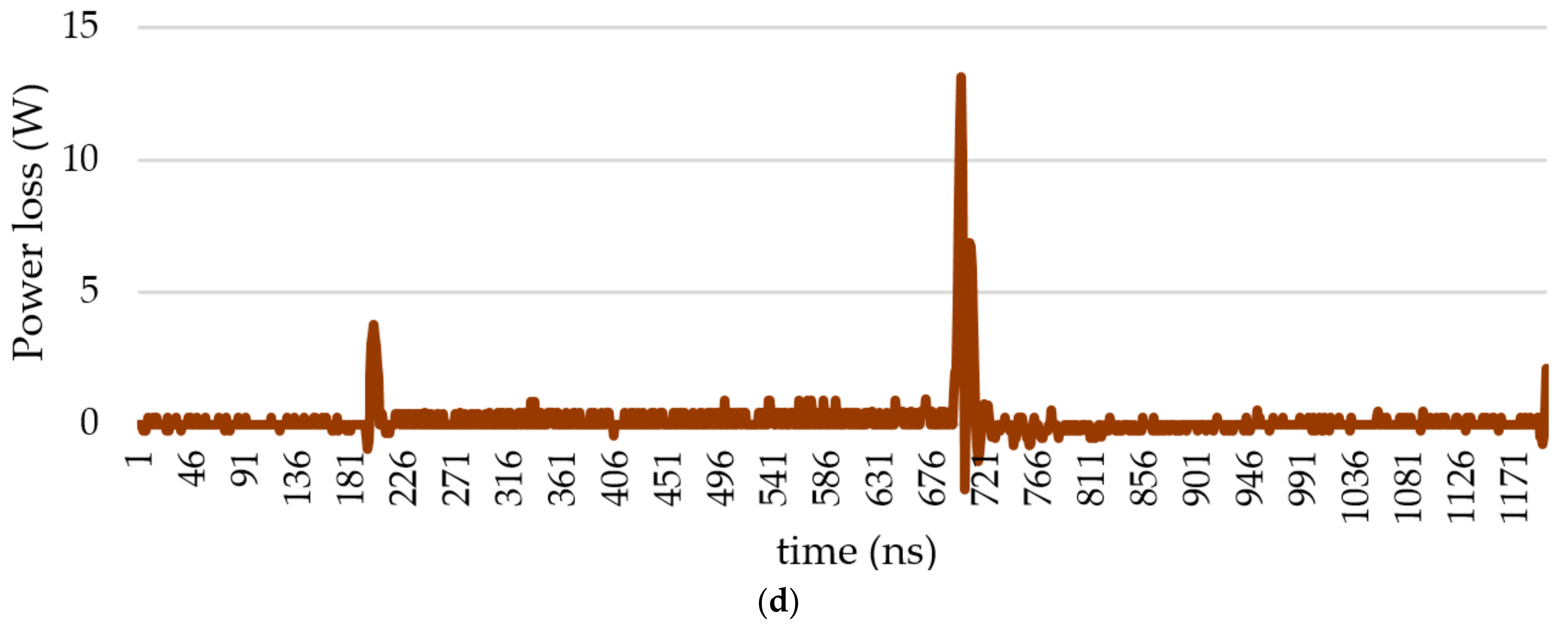
We have performed experiments of the synchronous buck converter using P-Cascode GaN HEMT to convert 12 V into an output of 5 V. The experiments follow the circuit shown in Figure 14, with the parameters indicated in Table 2. The power delivery is controlled by the duty ratio δ from the function generator Tektronix AFG31054. The experiment output for a switching frequency of 500 kHz and δ = 50% is shown in Figure 16, in which the drain-source voltage vsd,GaN (the orange line) of the GaN and the output voltage v1 = vsd,MOS (the blue line) are shown. Zooming in on the responses in the dotted rectangle area of the photo in Figure 16a, we draw the individual signals of the voltage and current measurements in Figure 16b,c. It is observed where there is still a minor shooting-through problem in Figure 16b, in that the PMOS turned on before the GaN turns off. It can also be observed that before PMOS turns off, the GaN HEMT is turned on at the synchronous time tick at around 700, as shown in Figure 16b,c. The shooting-through problem will induce the drain-source voltage to ring to the highest value, nearly 25 V, which is double the input voltage of 12 V. It is also observed for the switching loss in Figure 16d that the instantaneous power loss can be as high as 13.14 W although the shooting through persists only for ten nanoseconds. The switching loss is 0.04 W, calculated from taking integration of the multiplication of vsd,GaN of Figure 16b and id of Figure 16c within the time tick from 696 to 706, and then dividing the integration by the number of ticks for a switching period, which is one thousand in this case. It is due to the parasitic capacitance of both GaN HEMT and PMOS being small when they are in the off-state, as shown in Table 3. Furthermore, the single direction capacitor CG shown in Figure 10 in series with the gate of the PMOS has also reduced the input capacitance when it turns on. As a result, it yields a 98.3% efficiency.
The other experiment for switching frequency at 1 MHz and δ = 50% is shown in Figure 17 in which the drain-source voltage vsd,GaN (the orange line) of the GaN, the input current iD (the green line), and the gate voltage vG (the blue line) are shown. It is shown that GaN is turning on around vG = −7 V at the time tick around 583 (0.8 ns per tick). It is shown that GaN is turning off at the time tick around 1844. Before the GaN is turned-off, the PMOS was turned on and hence the current surged, resulting in a shooting-through problem. This experiment is via a Zener diode with a higher reverse breakdown voltage VZ to 11 V in Equations (17)–(23). As shown in Figure 17b, equivalently we had clamped the gate voltage vG up by 1 V relative to the threshold voltage VTg and VTp when VZ = 11 V. This will cause the output ringing according to Equations (12) and (13) and Figure 11. This output ringing will induce the input current to ring simultaneously during the GaN turning off, which results a larger switching loss. In Figure 18, with each time tick on the horizontal axis being 0.8 nanosecond, the switching losses for different Zener diodes are compared. All of the three configurations have a similar width on the top, but they are different on the bottom. As a result, the switching loss coefficient α in Equation (36) will be different when a different Zener diode is used. In our case study, the switching loss of VZ = 11 V is the worst of the three choices. It is also worth noting that no matter what the value of VZ, it can never find a snappy recovery nor uncontrolled high dIrr/dt when GaN turns on, as shown in Figure 17a,b. In the future, there may be implementation of the synchronous buck converter using two cascode D-mode GaNs to further reduce the EMI since, in some applications, the cost and weight of the filter can nullify the benefits of power efficiency improvement.
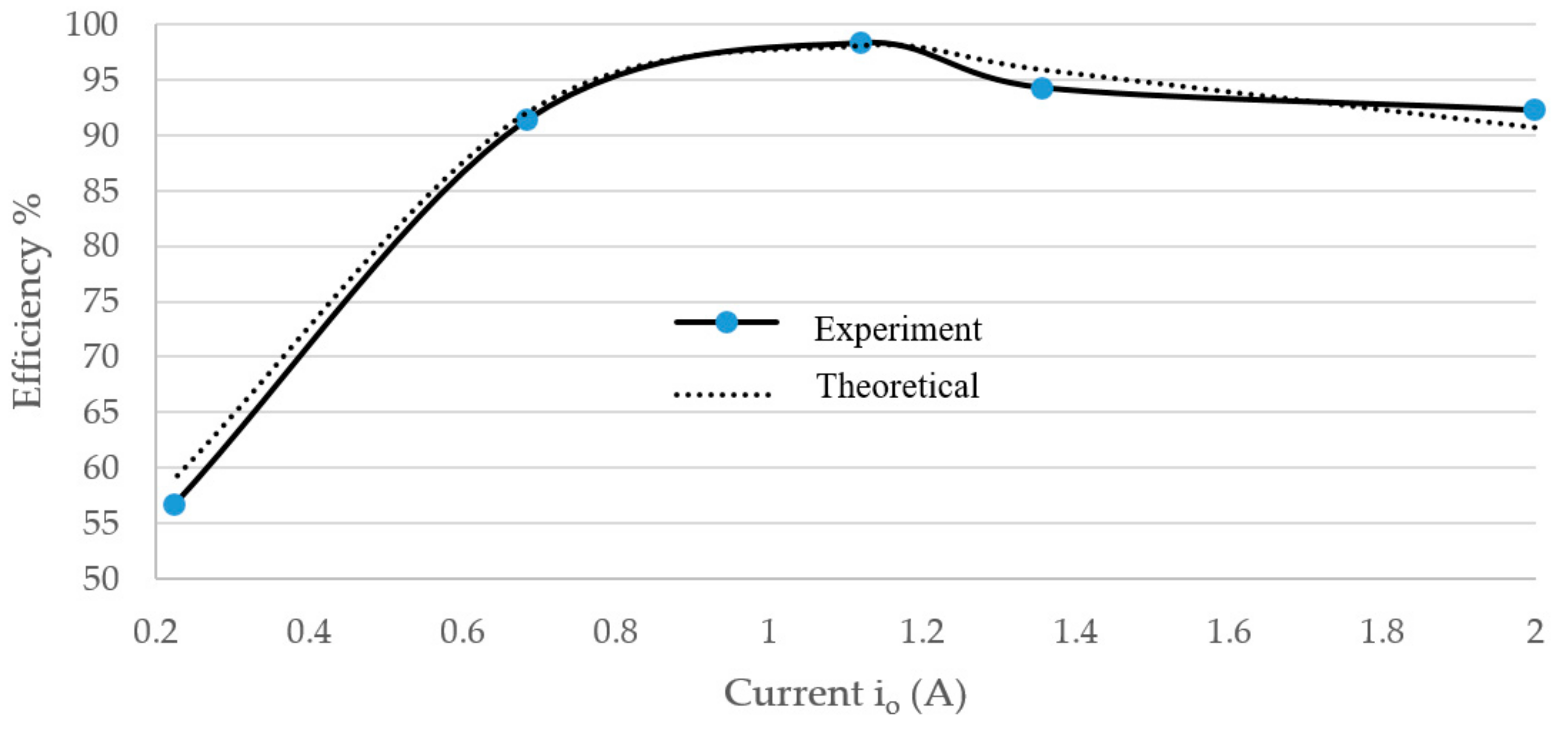
More experiments due to a different duty ratio δ at 500 kHz are summarized into Figure 19. There is a sink after a duty ratio of 60% that comes back again at a higher duty ratio. From Equation (34), we obtain that
β = 5/(2 × 47 × 10−6 × 500 × 103) = 0.11,
Io = (12/5)δ(1 + 0.11(1 − δ))
When the duty ratio is 10%, the current is measured as 223 mA and the efficiency is 56%, the ron is estimated around 200 mΩ at the deep saturation region, and VDD = 12 V. Compared to Equation (37), it is concluded that the switching loss factor α is around 0.044 from the following equation.
((1 − α/0.1) − 0.223 × 0.2/12) × 100 = 56
Substituting α = 0.01 + 0.1 × |δ − 0.5| and ron = (0.1 + 0.1δ) Ω into Equation (37) and providing that (ron,PMOS/R1) in Equation (33) reduced the actual amount of the current, we used the following equation to estimate the efficiency and compare the theoretical result also in Figure 19.
η = ((1 − α/δ) − 0.83·Ioron/VDD) × 100
In the experimental results analysis shown in Figure 20, we excluded the coil loss and capacitor loss because we want to clarify the P-Cascode GaN HEMT. When we actually calculate the power of the load, the output power is calculated from
Pout = IO2 R1
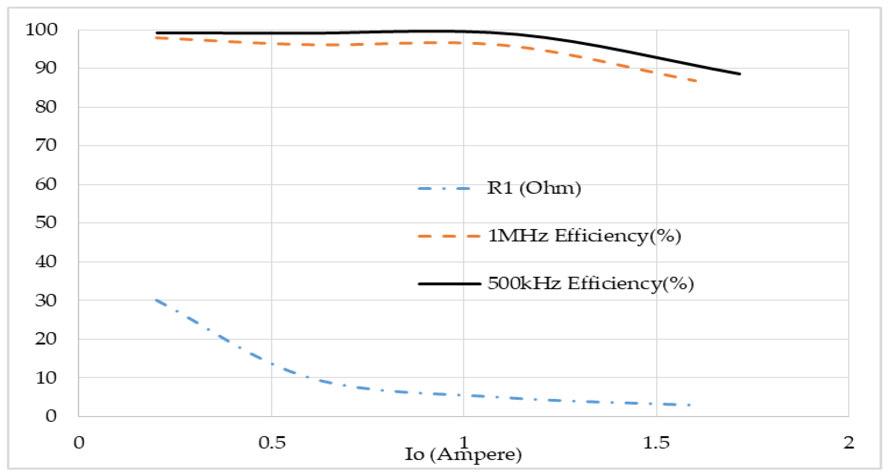
The efficiency is calculated from the power output divided by the power input, which is same as that of Figure 19. The result of the experiments subjected to the same load R1 = 5 Ω with 500 kHz and 1 MHz switching frequencies were compared and shown in Figure 20. The overall efficiency for 500 kHz is more than 92% at 20 W output and the overall efficiency for 1 MHz is 89% at 20 W output; however, it yields a better overall efficiency, which is 97% compared to 95% from the 500 kHz switching, at 5 W output. The reason why they are not compared in the same figure is because they were obtained by adjusting the duty ratio from 10% to 90% and the current readings for a different frequency are different according to Equations (34) and (35). The higher the frequency is applied to the switching, the lower the current output is.
The standard efficiency evaluation is measured by varying the load when fixing the switching frequency and the duty cycle. The result of the experiments subjected to different R1 loads with fixed duty at 50% are compared and shown in Figure 21. It can be observed from Equation (36) that the total power loss increases when the output current increased. It is also observed that the switching loss factor α in Equation (36) will increase as the switching frequency increases. The power output in the experiment can be calculated by Equation (42), which are from 1 to 10 W. The standard efficiency evaluation based on a 1 MHz switching frequency was also used to compare the simulation shown in Figure 15 and Equation (33). A comparison among the experiment, simulation, and Equation (33) is shown in Table 4. The Equation provides a higher output current than both the experiment and simulation do. The efficiency predicted by the simulation is lower than the experiment, which may be as a result of the output from the gate driver, which is the LM5114 PSpice model downloaded from TI Instrument®, not responding as fast as the practical ones subjected to the switching of the input signal vpwm.
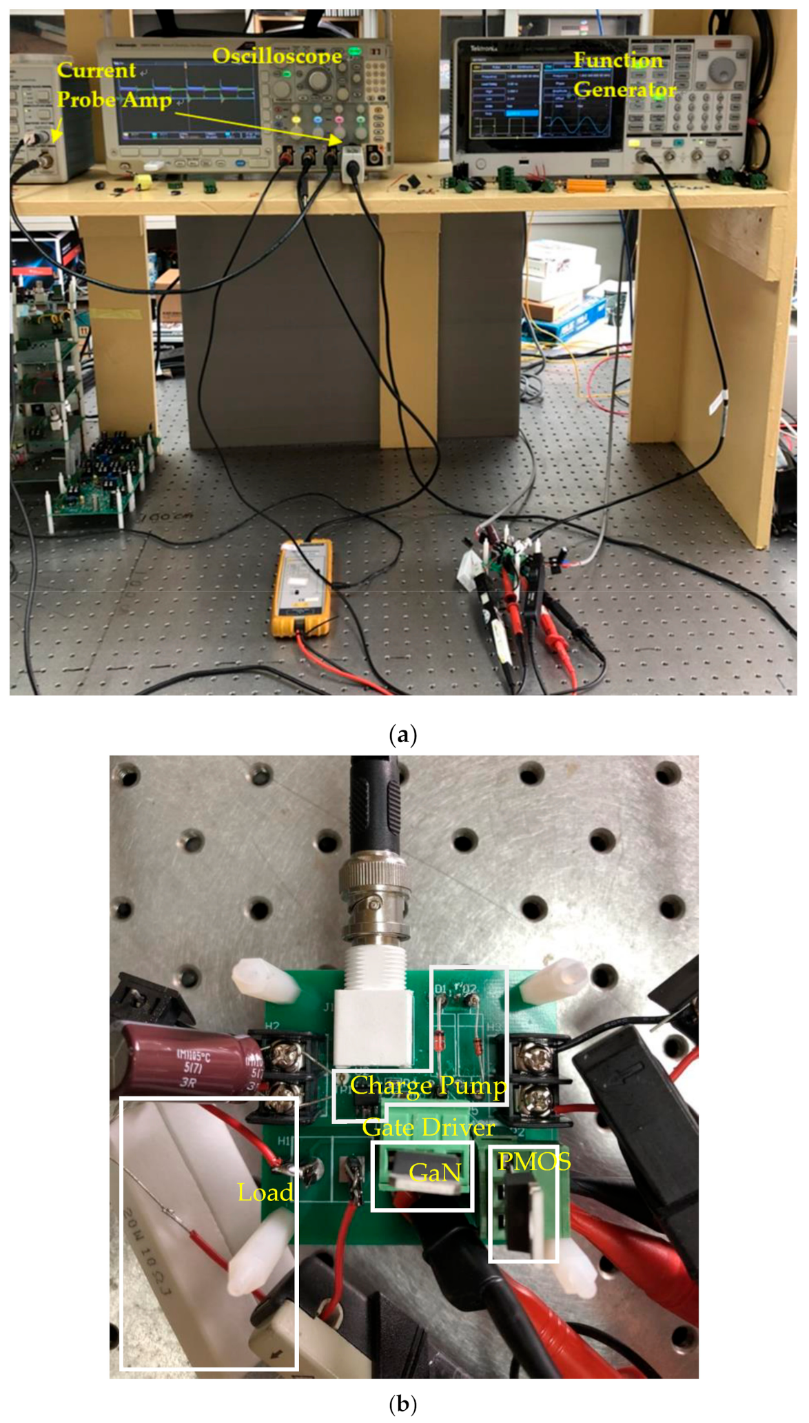
The oscilloscope we used in the experiment is a Tektronix MDO 3054, which has four inputs: we used two voltage probes and two current probes, measuring simultaneously the signals. The efficiency evaluation is influenced both by the error on the measured input power and on the measured output power despite the measure data being synchronized. In the literature [28], dealing with extreme efficiency in power electronics, the measurement data are acquired in the two-chamber calorimeter that handles the temperature control. In this paper, we only use the air conditioner to maintain a stable room temperature and performed the experiments intermittently to reduce the temperature effect on the experiments. As indicated in Figure 22a, we measured four signals, including vsd,GaN, vsd,PMOS, id, and io, and added the two measures vsd,GaN and vsd,PMOS together into the voltage input. The power input is calculated by the average of the multiplication on the 10,000 samples of 6 to 10 periods of switching, as follows.
Pin = ∑ id (vsd,GaN + vsd,PMOS)
and
Pout = ∑ iO × vsd,PMOS
The high efficiency part of the experiment is done by averaging the efficiency calculations from different experiments with the identical setting. In was hopeful, at least theoretically, that the variance of the efficiency measure be reduced by the number of times of measurements.
The photo of the circuit in the experiment is shown in Figure 22b. Since all of the components used are rather standard and handy for the SiP packaging, it may be implemented in an IC form factor later.

4. Conclusions

An innovative design of a new GaN HEMT synchronous buck converter is proposed. This synchronous buck converter is associated with a PMOS transistor; thus, it will need only one single gate drive to perform the DC/DC conversion, which is suitable for the point of load (POL) applications. In order to solve the shooting-through problem when only a single gate drive is used, the characteristics of both GaN HEMT and the PMOS must be studied. To compensate for the differences between GaN HEMT and the PMOS, an additional gate drive design is necessary. To fulfill the transistor matching, we used a single direction capacitor that prolonged the turn-on delay time in the PMOS. Furthermore, to prevent the output spike of the GaN HEMT during the turn-on period, we needed to reduce the gate resistance and equivalently to increase α in the above equation. Since the GaN HEMT is used on the high side, a Zener diode is used instead of a DC battery to lift the voltage, which is identical to the breakdown voltage of the Zener diode from the original charge-pump gate drive output. The circuit was implemented and tested. The result in the proposed circuit specification shows that the P-Cascode GaN HEMT efficiency is higher than 98% at a switching frequency 500 kHz and duty ratio δ = 50%. When the output is up to 20 W, the overall efficiency can be higher than 92%. In the future, we will find a better-matched PMOS to achieve a higher switching frequency for the NCTU GaN HEMT; i.e., the turn-on and turn-off voltage must have a good match for the D-mode GaN HEMT and the parasitic capacitance of the PMOS must be made smaller to match the parasitic capacitance of the GaN HEMT. Nevertheless, the SPICE simulation model must also be carefully studied in order to predict the better design requirements.

Author Contributions

Conceptualization, E.Y.C. and W.-H.C.; methodology, C.-C.W.; software, C.-C.W.; validation, C.-Y.L., G.-B.W. and C.-C.W.; formal analysis, Y.-T.S.; resources, G.-B.W.; writing—original draft preparation, W.-H.C.; writing—review and editing, C.-C.W.; visualization, E.Y.C.; supervision, E.Y.C.; project administration, E.Y.C.; funding acquisition, W.-H.C. All authors have read and agreed to the published version of the manuscript.

Funding

This research was funded by Ministry of Science and Technology, R.O.C, grant number MOST(NSC)109-3116-F009-001-CC1.

Institutional Review Board Statement

Not applicable.

Informed Consent Statement

Not applicable.

Data Availability Statement

Data sharing is not applicable.

Acknowledgments

This work was supported by Ministry of Science and Technology, R.O.C. The authors would also like to thank CSD Lab for providing the fabrication of D-Mode MIS-HEMT chips.

Conflicts of Interest

The authors declare no conflict of interest.

References

  1. Abdelrahman, A.S.; Erdem, Z.; Attia, Y.; Youssef, M.Z. Wide bandgap devices in electric vehicle converters: A performance survey. Can. J. Electr. Comput. Eng. 2018, 41, 45–54. [Google Scholar]
  2. Nan, C.; Ayyanar, R.; Xi, Y. A 2.2-MHz active-clamp buck converter for automotive applications. IEEE Trans. Power Electron. 2017, 33, 460–472. [Google Scholar] [CrossRef]
  3. He, J.; Cheng, W.C.; Wang, Q.; Cheng, K.; Yu, H.; Chai, Y. Recent Advances in GaN-Based Power HEMT Devices. Adv. Electron. Mater. 2021, 7, 2001045. [Google Scholar] [CrossRef]
  4. Nikoo, M.S.; Jafari, A.; Perera, N.; Matioli, E. New insights on output capacitance losses in wide-band-gap transistors. IEEE Trans. Power Electron. 2019, 35, 6663–6667. [Google Scholar] [CrossRef]
  5. Dalla Vecchia, M.; Ravyts, S.; Van den Broeck, G.; Driesen, J. Gallium-Nitride Semiconductor Technology and Its Practical Design Challenges in Power Electronics Applications: An Overview. Energies 2019, 12, 2663. [Google Scholar] [CrossRef] [Green Version]
  6. Rodriguez, J.; Lamar, D.G.; Roig, J.; Rodriguez, A.; Bauwens, F. Improving the third quadrant operation of superjunction MOSFETs by using the cascode configuration. IEEE Trans. Power Electron. 2018, 34, 2726–2738. [Google Scholar] [CrossRef] [Green Version]
  7. Xu, J.; Gu, L.; Ye, Z.; Kargarrazi, S.; Rivas-Davila, J.M. Cascode GaN/SiC: A wide-bandgap heterogenous power device for high-frequency applications. IEEE Trans. Power Electron. 2019, 35, 6340–6349. [Google Scholar] [CrossRef]
  8. Lyu, G.; Wang, Y.; Wei, J.; Zheng, Z.; Sun, J.; Zhang, L.; Chen, K.J. A Normally-off Copackaged SiC-JFET/GaN-HEMT Cascode Device for High-Voltage and High-Frequency Applications. IEEE Trans. Power Electron. 2020, 35, 9671–9681. [Google Scholar] [CrossRef]
  9. Jiang, S.; Lee, K.B.; Zaidi, Z.H.; Uren, M.J.; Kuball, M.; Houston, P.A. Field Plate Designs in All-GaN Cascode Heterojunction Field-Effect Transistors. IEEE Trans. Electron Devices 2019, 66, 1688–1693. [Google Scholar] [CrossRef]
  10. Huang, X.; Du, W.; Lee, F.C.; Li, Q.; Liu, Z. Avoiding Si MOSFET avalanche and achieving zero-voltage switching for cascode GaN devices. IEEE Trans. Power Electron. 2015, 31, 593–600. [Google Scholar] [CrossRef]
  11. Huang, X.; Li, Q.; Liu, Z.; Lee, F.C. Analytical loss model of high voltage GaN HEMT in cascode configuration. IEEE Trans. Power Electron. 2013, 29, 2208–2219. [Google Scholar] [CrossRef]
  12. Xue, P.; Maresca, L.; Riccio, M.; Breglio, G.; Irace, A. Investigation on the short-circuit oscillation of cascode GaN HEMTs. IEEE Trans. Power Electron. 2019, 35, 6292–6300. [Google Scholar] [CrossRef]
  13. Chen, Y.; Wang, R.; Liu, X.; Kang, Y. Gate-Drive Power Supply With Decayed Negative Voltage to Solve Crosstalk Problem of GaN Synchronous Buck Converter. IEEE Trans. Power Electron. 2020, 36, 6–11. [Google Scholar] [CrossRef]
  14. Lyu, G.; Wang, Y.; Wei, J.; Zheng, Z.; Chen, K.J. Dv/Dt-Control of 1200-V Normally-off SiC-JFET/GaN-HEMT Cascode Device. IEEE Trans. Power Electron. 2020, 36, 3312–3322. [Google Scholar] [CrossRef]
  15. Xie, Y.; Chen, C.; Huang, Z.; Liu, T.; Kang, Y.; Luo, F. High frequency conducted EMI investigation on packaging and modulation for a Sic-based high frequency converter. IEEE J. Emerg. Sel. Top. Power Electron. 2019, 7, 1789–1804. [Google Scholar] [CrossRef]
  16. Chou, P.-C.; Chen, S.-H.; Hsieh, T.-E.; Cheng, S.; Del Alamo, J.A.; Chang, E.Y. Evaluation and Reliability Assessment of GaN-on-Si MIS-HEMT for Power Switching Applications. Energies 2017, 10, 233. [Google Scholar] [CrossRef] [Green Version]
  17. Elangovan, S.; Cheng, S.; Chang, E.Y. Reliability characterization of gallium nitride MIS-HEMT based cascode devices for power electronic applications. Energies 2020, 13, 2628. [Google Scholar] [CrossRef]
  18. Chou, P.C.; Hsieh, T.E.; Cheng, S.; Del Alamo, J.A.; Chang, E. Comprehensive dynamic on-resistance assessments in GaN-on-Si MIS-HEMTs for power switching applications. Semicond. Sci. Technol. 2018, 33, 055012. [Google Scholar] [CrossRef] [Green Version]
  19. Chen, S.H.; Chou, P.C.; Cheng, S. Evaluation of thermal performance of packaged GaN HEMT cascode power switch by transient thermal testing. Appl. Therm. Eng. 2016, 98, 1003–1012. [Google Scholar] [CrossRef]
  20. Chou, H.P.; Cheng, S. Thermal performance evaluation of cascode Paralleled-GaN-HEMTs packaging for high power switching applications. J. Therm. Sci. Technol. 2017, 12, JTST0022. [Google Scholar] [CrossRef] [Green Version]
  21. Wu, C.C.; Jeng, S.L. Comparison of Parasitic Capacitances of Packaged Cascode Gallium Nitride Field-effect Transistors. Sens. Mater. 2018, 30, 453–461. [Google Scholar]
  22. Wu, C.C.; Jeng, S.L. Simulation Model Development for Packaged Cascode Gallium Nitride Field-Effect Transistors. Crystals 2017, 7, 250. [Google Scholar] [CrossRef] [Green Version]
  23. Lin, Y.C.; Chen, S.H.; Lee, P.H.; Lai, K.H.; Huang, T.J.; Chang, E.Y.; Hsu, H.-T. Gallium Nitride (GaN) High-Electron-Mobility Transistors with Thick Copper Metallization Featuring a Power Density of 8.2 W/mm for Ka-Band Applications. Micromachines 2020, 11, 222. [Google Scholar] [CrossRef] [Green Version]
  24. Weng, Y.C.; Wu, C.C.; Chang, E.Y.; Chieng, W.H. Minimum Power Input Control for Class-E Amplifier Using Depletion-Mode Gallium Nitride High Electron Mobility Transistor. Energies 2021, 14, 2302. [Google Scholar] [CrossRef]
  25. Ishibashi, T.; Okamoto, M.; Hiraki, E.; Tanaka, T.; Hashizume, T.; Kikuta, D.; Kachi, T. Experimental validation of normally-on GaN HEMT and its gate drive circuit. IEEE Trans. Ind. Appl. 2014, 51, 2415–2422. [Google Scholar] [CrossRef]
  26. Yoshida, K.; Ishii, T.; Nagagata, N. Zero voltage switching approach for flyback converter. In Proceedings of the Fourteenth International Telecommunications Energy Conferences, Washington, DC, USA, 4–8 October 1992; pp. 324–329. [Google Scholar]
  27. Liu, C.Y.; Wang, G.B.; Wu, C.C.; Chang, E.Y.; Cheng, S.; Chieng, W.H. Derivation of the Resonance Mechanism for Wireless Power Transfer Using Class-E. Amplifier. Energies 2021, 14, 632. [Google Scholar] [CrossRef]
  28. Kolar, J.W.; Krismer, F.; Lobsiger, Y.; Mühlethaler, J.; Nussbaumer, T.; Miniböck, J. Extreme Efficiency Power Electronics. In Proceedings of the International Conference of Integrated Power Electronics Systems (CIPS 2012), Nuremberg, Germany, 6–8 March 2012; pp. 1–22. [Google Scholar]
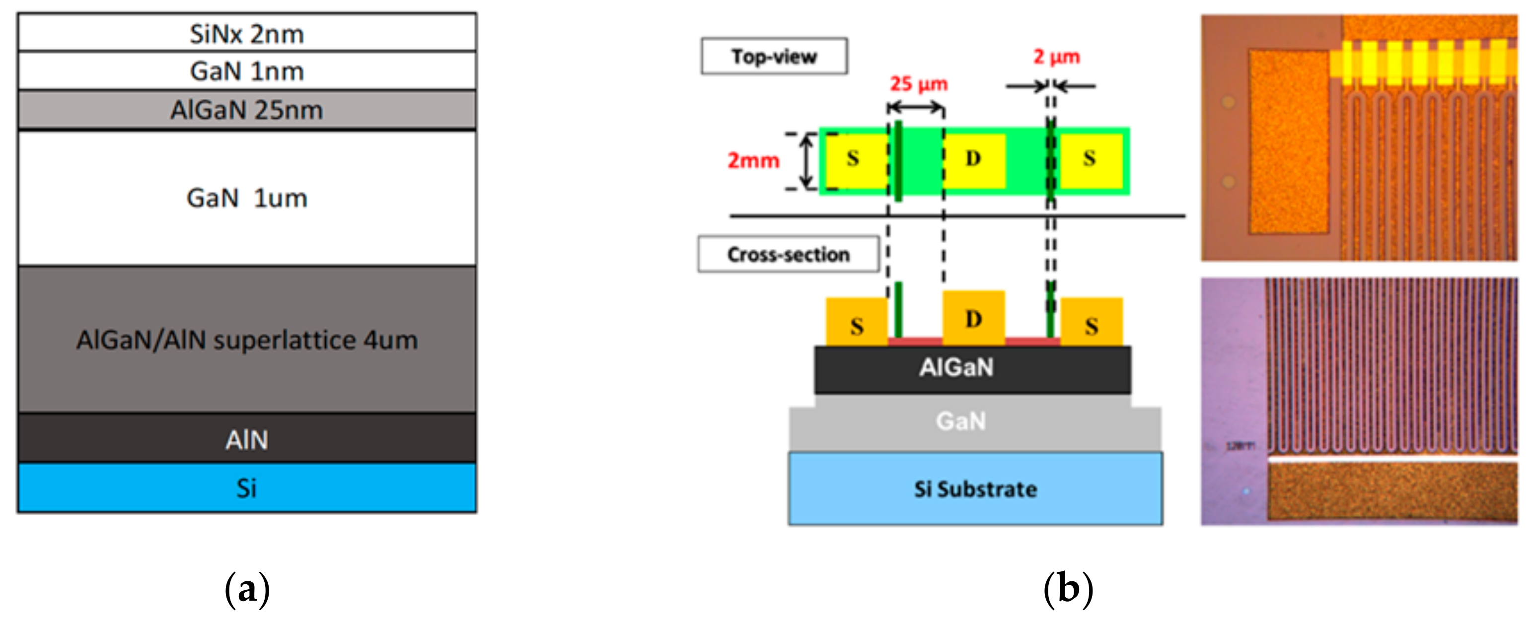
Figure 1. (a) Cross-section of the D-mode GaN MIS-HEMT; (b) 120 mm D-mode GaN MIS-HEMT devices.
Energies 14 03477 g001
Figure 2. The field plate of the D-mode GaN MIS-HEMT.
Energies 14 03477 g002
Figure 3. The triangular wave on–off experiment setups.
Energies 14 03477 g003
Figure 4. The triangular wave on–off traces of a D-mode GaN HEMT.
Energies 14 03477 g004
Figure 5. Results of the triangular wave on–off experiment of GaN HEMT at (a) 1 kHz and (b) 800 kHz.
Energies 14 03477 g005
Figure 6. Cascode GaN HEMT: (a) the cascode circuit; (b) the packaged device.
Energies 14 03477 g006
Figure 7. P-Cascode GaN HEMT Module.
Energies 14 03477 g007
Figure 8. Result of the triangular wave on–off experiment (II) of the PMOS at (a) 1 kHz and (b) 800 kHz.
Energies 14 03477 g008
Figure 9. Operational region of the gate voltage for P-Cascode GaN HEMT.
Energies 14 03477 g009
Figure 10. P-Cascode GaN HEMT Module.
Energies 14 03477 g010
Figure 11. Operational region of gate voltage for P-Cascode GaN HEMT.
Energies 14 03477 g011
Figure 12. The biased charge-pump gate drive.
Energies 14 03477 g012
Figure 13. The conventional interlock switching to prevent the shooting-though problem.
Energies 14 03477 g013
Figure 14. Synchronous buck converter using the P-Cascode GaN HEMT.
Energies 14 03477 g014
Figure 15. SPICE simulation model for the synchronous buck converter.
Energies 14 03477 g015
Figure 16. The experimental result for 12 V to 6.5 V step down at a switching frequency of 500 kHz and δ = 50%: (a) oscilloscope photo; (b) vsd of PMOS and vsd of the GaN HEMT data plot; (c) current io and id plot; and (d) the instantaneous power loss ((bd): 2 ns per tick).
Energies 14 03477 g016aEnergies 14 03477 g016b
Figure 17. The experimental result for the 12 V to 6 V step down at a switching frequency of 1 MHz with (a) VZ = 10 V and (b) VZ = 11 V (0.8 ns per tick).
Energies 14 03477 g017
Figure 18. Comparison of the switching losses due to different Zener diodes (0.8 ns per tick).
Energies 14 03477 g018
Figure 19. The P-Cascode GaN HEMT efficiency at a 500 kHz switching frequency vs. a different output current via duty control.
Energies 14 03477 g019
Figure 20. The power to load and overall efficiency at the 500 kHz and 1 MHz switching frequencies vs. the different output currents via duty control.
Energies 14 03477 g020
Figure 21. The power efficiency of the 500 kHz and 1 MHz switching frequencies with δ = 50% vs. different loadings.
Energies 14 03477 g021
Figure 22. (a) Experimental setup and (b) photo of the circuit in the experiment.
Energies 14 03477 g022
Table 1. Characteristics summary of the D-mode GaN HEMT.
SymbolUnitDescriptionValuevDS
0 V12 V
vGS,ON (or −VTg)VTurn-on voltage (All)−4
Turn-off voltage (800 kHz switching)−4
Turn-off voltage (1 kHz switching)−7
CDSpFParasitic capacitance 7570
CGDpFParasitic capacitance 245220
CGSpFParasitic capacitance 140140
VGS,maxVMaximum gate-source voltage8
VDS,BDVDrain-source breakdown voltage35
id,maxAMaximum drain current60
Ld + LsnHStray Inductance, drain to source (100 kHz)80
Ld + LsnHStray Inductance, source to drain (100 kHz)120
Table 2. Summary of the synchronous buck converter.
SymbolUnitDescriptionValue
L1μHBuck Converter47
C1μF47
R1Ω5
PMOSSTD10P6F6P-Cascode GaN HEMT Module-
GaN HEMTNCTUTable 1
CppF1000
CGnF100
RG,pΩGate driver30
RG,nΩ51
CCnF100
Zener VzVGate driver, Break down voltage10
VDDVVoltage Source12
VGGV20
Table 3. The input parasitic capacitance Ciss at a switching frequency of 1 MHz.
SymbolUnitDescriptionValue
0 V12 V
CisspFGaN HEMT390270
CisspFPMOS450370
Table 4. Comparison among the experiment, simulation, and Equation (33).
R1 (Ohm)Io (Ampere)
ExperimentSimulation
Figure 15
Equation (33)
300.201350.1920.199
100.5490.560.594
51.1111.0971.176
31.6141.761.935
R1(Ohm)Efficiency
ExperimentSimulation
Figure 15
-
309892-
1096.193.3-
596.286.4-
386.981.5-
Publisher’s Note: MDPI stays neutral with regard to jurisdictional claims in published maps and institutional affiliations.