Article

Grown and Characterization of ZnO Aligned Nanorod Arrays for Sensor Applications

by
Arkady N. Redkin
,
Eugene E. Yakimov
,
Maria V. Evstafieva
and
Eugene B. Yakimov
*
Institute of Microelectronics Technology RAS, 6 Academician Ossipyan str., 142432 Chernogolovka, Russia
*
Author to whom correspondence should be addressed.
Energies 2021, 14(13), 3750; https://doi.org/10.3390/en14133750
Submission received: 13 May 2021 / Revised: 3 June 2021 / Accepted: 17 June 2021 / Published: 22 June 2021

Abstract

:
ZnO nanorods are promising materials for many applications, in particular for UV detectors. In the present paper, the properties of high crystal quality individual ZnO nanorods and nanorod arrays grown by the self-catalytic CVD method have been investigated to assess their possible applicationsfor UV photodetectors. X-ray diffraction, Raman spectroscopy and cathodoluminescence investigations demonstrate the high quality of nanorods. The nanorod resistivity and carrier concentration in dark is estimated. The transient photocurrent response of both as grown and annealed at 550 °C nanorod array under UV illumination pulses is studied. It is shown that annealing increases the sensitivity and decreases the responsivity that is explained by oxygen out-diffusion and the formation of near surface layer enriched with oxygen vacancies. Oxygen vacancy formation due to annealing is confirmed by an increase of green emission band intensity.

1. Introduction

Zinc oxide, a well-known direct bandgap II–VI semiconductor, is a material with large exciton binding energy (60 meV) and a wide bandgap (Eg ~ 3.37 eV) [1], suitable for short wavelength optoelectronic applications [2]. It is a promising material for fabricating photonic [2,3], optical [4,5,6], electronic [7,8] and photovoltaic devices [9,10]. Additionally, ZnO is transparent to visible light and can be made highly conductive by doping [11,12]. The non-centrosymmetry in ZnO wurtzite structure and the polarity developed along the c axis make this material piezoelectric, which, in combination with its large electromechanical coupling, results in strong piezoelectric and pyroelectric properties useful in piezoelectric sensors [13,14] and nanogenerators [15,16]. The ferromagnetism of doped [17] and undoped ZnO [18] makes it a promising material for spintronics. Additional useful advantages of zinc oxide include low toxicity, chemical stability, electrochemical activity, making it a promising material for biosensors, and biomedical applications [19,20].
In the strict sense, zinc is not a transition metal as it has d10s2 electronic configuration with a completely filled d-shell and can be classified as post-transition metal. However, it exhibits many properties similar to those of transition metals and sometimes it is often convenient to include this element in a discussion of the transition elements. In zinc oxide, s electrons are strongly pulled by oxygen and consequently the structural, physical and chemical properties are mostly determined by the d electrons, in certain sense similar to transition metal oxides.
Miniaturization in electronics and development of different photonic devices requires a new generation of cheap, energy-efficient, nano- or submicron sized semiconductor lasers. One-dimensional (1D) ZnO nanocrystals have a perfect structure and a developed surface, which gives them certain advantages when used in the abovementioned practical applications [5,16]. In this regard, the ordered arrays of zinc oxide nanorods (NR) obtained by various methods are of great interest to researchers [21,22]. To obtain ZnO nanorods, various methods were used, such as hydrothermal synthesis, solvothermal method, sol-gel method, chemical vapor deposition, organometallic chemical vapor deposition, magnetron sputtering, laser ablation, etc. [2,21,23]. Most of these processes are carried out at relatively low temperatures that lead to a decrease in the cost of the structures but increases inthe number of defects. Therefore, despite the abundance of methods, the synthesis of high-quality ZnO NRs with a perfect structure is not an easy task. The properties of ZnO NRs can vary greatly, even within the same method of synthesis. In [24] the original self-catalytic CVD procedure for growing zinc oxide nanorod arrays was developed. One of the advantages of this method is the possibility to deposit ordered arrays of high-quality single-crystal ZnO nanorods both on silicon substrates of various orientations and on inexpensive transparent glass substrates [25], which makes it attractive for practical applications. The method was developed to grown high quality nanorods for use as a laser medium. It was interesting to study the performance of such nanorods as UV sensors.
In present work, arrays of ZnO nanorods were grown by the self-catalytic CVD procedure. The properties of nanorods were investigated to assess their possible applications for UV photodetectors. The performance of the UV sensors depends both on the state of the zinc oxide surface and on the concentration of intrinsic defects, which strongly depends on synthesis conditions and/or by post-synthesis treatment.

2. Materials and Methods

The NR arrays were synthesized in a flow type two-zone quartz reactor in accordance with the previously developed method [24,25,26]. A charge of granulated high-purity (99.99%) zinc was placed in the first (evaporation) zone, and substrates were placed in the second (synthesis) zone. Si {100}, fused silica and glass wafers were used as substrates. Synthesis was carried out at a reduced pressure under the conditions of continuous evacuation. The pressure in the reactor was kept at a level of 103 Pa. The process was carried out at temperatures of 610 °C and 550 °C in the evaporation and synthesis zones, respectively. During the process, zinc was evaporated in the first zone, from which zinc vapor arrived at the second cooler zone, where it was partially condensed, forming an array of zinc nanodrops on the substrates, which are sufficiently uniform in size. These Zn drops serve as a catalyst, in contrast to the usual CVD process in which a noble metal (gold) is used as a catalyst. Further, when a high-purity oxygen–argon mixture (15% O2) enters the growth zone, its chemical interaction with liquid zinc occurs. Due to the reaction of zinc with oxygen, zinc oxide nanocrystals were deposited onto the substrates under the zinc droplets. Further, when oxygen enters the growth zone, its chemical interaction with liquid zinc occurs. The formed oxide is dissolved in a drop of zinc to form a supersaturated solution, from which solid ZnO crystallizes at the metal/substrate interface. The gas mixture was supplied to the reactor with a rate of 6 L/h. The synthesis was carried out for 20–30 min with the zinc consumption of 12–15 g/h. The diameter of the growing NRs corresponds to the diameter of the liquid zinc drop. Using this procedure, high-quality ZnO NR arrays were grown, the diameter and length of which can be varied by changing the synthesis conditions (duration, reagent consumption, etc.). The above procedure allows us to synthesize arrays of well faceted vertically aligned single-crystal NRs with a 150–250 nm diameter and up to 10 μm length. To obtain individual nanorods they were separated from the substrate by ultrasonic treatment and transferred on a silicon substrate.
The cathodoluminescence (CL) investigations of arrays and individual nanorods of different size and geometry were carried out in the JSM 6490 (JEOL) SEM equipped with the MonoCL3 system (Gatan) and with the Hamamatsu photomultiplier as a detector. The investigations were carried out in the temperature range from 90 to 300 K. In the most cases the beam energy in the range from 10 to 20 kV and beam current of 0.1–1 nA were used for the CL measurements.
The crystallinity of NRs was examined by X-ray diffractometry (Θ–2Θ) in the scheme of a two-crystal diffractometer on a laboratory BRUKER D8 Discover X-ray source with a rotating copper anode (CuKα radiation, λ = 1.54 Ǻ). The Raman spectra of the samples were studied using a Bruker Sentera RAMAN microscope under the excitation by a 532 nm solid-state laser.
To study the photoresponse of nanorod arrays vertically oriented nanorods were grown on quartz substrates coated with a thin polycrystalline ZnO film. The diameter and density of nanorods as estimated by the SEM was of 150 nm and 4 × 108 cm−2, respectively. For current measurements a quartz plate with two indium contacts deposited in the form of strips with a length of 2 mm and a distance of 3 mm between them was pressed to the nanorod arrays. The transient photocurrent response of samples was measured at a bias voltage of 30 V using UV lamp with the emission maximum of about 370 nm and a power of 4 W.

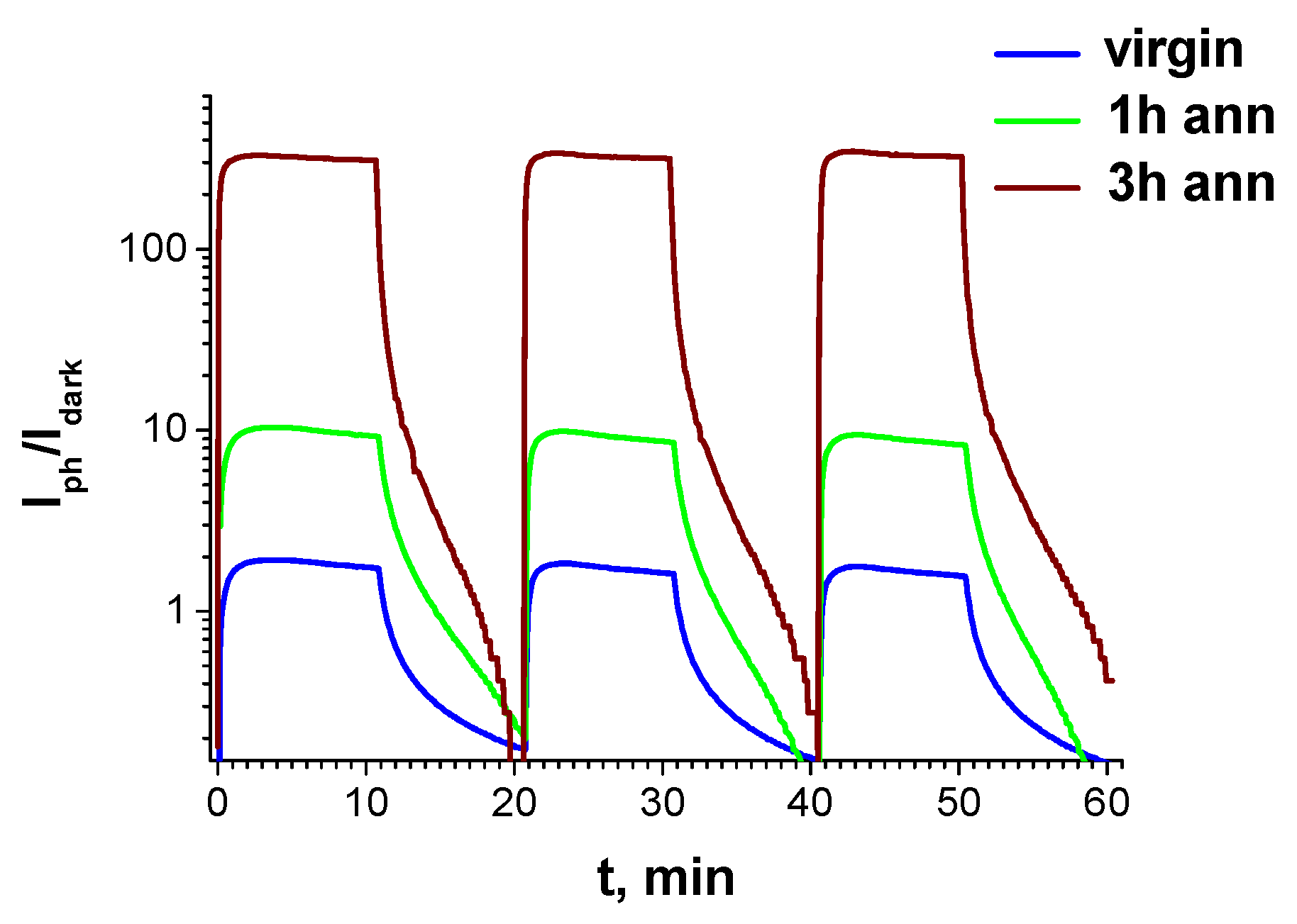
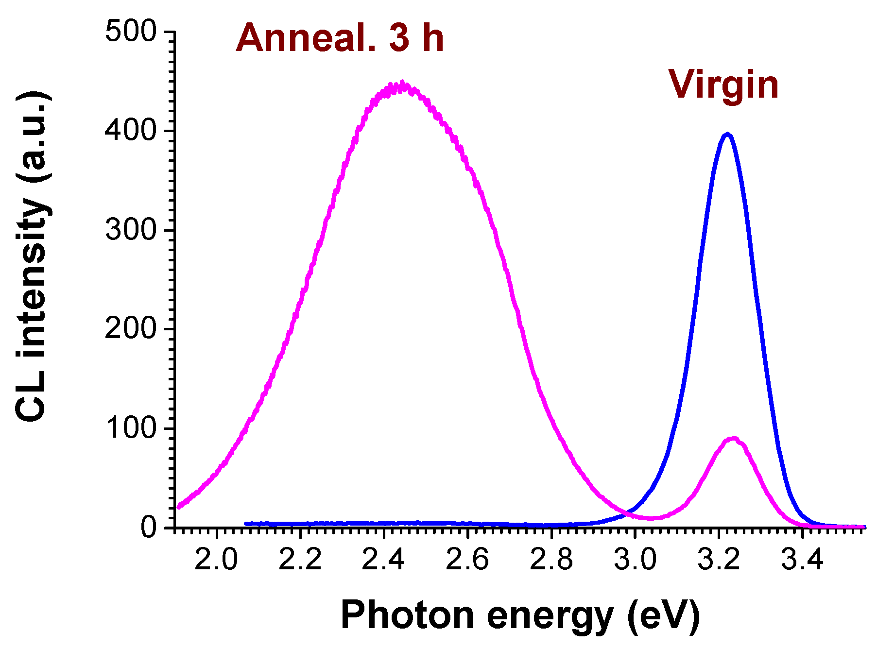
3. Results and Discussion

The typical SEM images of studied NRs are presented in Figure 1. It is seen that the most of NRs are aligned perpendicular to the substrate. The diffractograms of the ordered arrays of ZnO NRs show only the (002) and (004) reflections (Figure 2), which confirms the growth direction of along the c-axis. The similar patterns were observed on arrays grown on both single crystal silicon and quartz substrates. The full width at half maximum of (002) peak for these arrays is of 10–12′, which indicates that the nanorods have a perfect crystal structure and are well aligned.
The high crystal quality of NRs was also confirmed by the Raman and CL spectra. The Raman spectra demonstrate the high crystal quality of the sample wurtzite structure (Figure 3). The low-frequency E2 (low) mode is mainly associated with nonpolar oscillations of the heavier Zn sublattice, whereas the high-frequency E2 (high) mode is mainly associated with the displacement of lighter oxygen atoms. The modes A1 and E1 are split into longitudinal (LO) and transverse (TO) optical components. With the exception of LO modes, all Raman active phonon modes are clearly identified in the measured spectrum. The full width at half maximum and the position of the peaks E2 (low) and E2 (high) are comparable to the values for bulk crystals of ZnO [27].
The CL studies of nanorod arrays showed that the spectrum consisted of two emission bands: near-bandedge (NBE) UV and green (2.4–2.5 eV), while the intensity of the first, as a rule, significantly exceeded the intensity of the second one. Despite numerical studies, the origin of green emission band remained divisive [28], although in the structures, which are not intentionally doped, it was usually associated with intrinsic point defects, in particular with oxygen vacancies. The low green band intensity indicates a high crystalline perfection of nanorods grown. Moreover, these means that the nanorods are stoichiometric or, as might be expected, are zinc rich. It was observed that the form and size of nanorods can vary depending on the growth conditions. A variation of nanorod size and form led to a change of NBE band form and of green band intensity. As an example, the UV CL spectra measured in the temperature range from 90 to 300 K on an individual nanorod and on nanorods grown together in the form of a comb are shown in Figure 4 and Figure 5. It is seen that at low temperature the excitonic lines are well resolved, however, their relative intensities depend on the nanorod form. This can be explained under an assumption that some excitonic modes fall into resonance inside the nanorods. At room temperature the excitonic modes are not resolved, nevertheless, it should be noted that the emission maximum for the individual nanorod is shifted to the higher energy by about 30 meV according the spectrum of the comb-like structure. It should be noted that the similar dependence on the nanorod size and form was observed in many papers; however, its cause has not yet been conclusively established [28,29,30].
To study the electrical and photoelectrical properties of single nanorods they were shaken off in an ultrasonic bath on a substrate with several preprepared In contacts and then places, in which the contacts were connected by only one nanorod, were found in a SEM (Figure 6). V-A curves measured on such nanorod in dark and under UV illumination are shown in Figure 7. It is seen that both dependences are practically linear, thus the contacts are practically ohmic or their resistance is lower than that of NR that correlates with [31]. The dark resistance is about 6.5 × 10⁸ Ohm, that allows to estimate the resistivity as 1.3 × 10⁴ Ohm×cm. If the electron mobility is assumed of 500 cm2/(V×s), the dopant concentration can be estimated as about 1012 cm−3. This value should be considered as the lower limit for the concentration because the contact resistance and a possible decrease of effective NR cross-section due to near surface band bending could increase the apparent resistance of NRs. Under UV illumination the resistance decreases by about 65 times, i.e., the detector sensitivity equals to Iph/Idark, where Iph and Idark are the photo- and dark current values, respectively, is of 65. The estimation of the responsivity shows that at a bias of 0.2 V it exceeds 500 A/W. Such high sensitivity and responsivity values can be expected for NRs because it is widely accepted that the photocurrent gain in short-length photodetectors is proportional to τ/tr, where τ and tr are the excess carrier lifetime and the carrier transit time, respectively [32], therefore it can reach high values in micron size structures. However, in spite of very high sensitivity and responsivity values photodetectors based on single NRs are unlikely to find wide practical application in the near future. Due to the complexity of fabricating structures based on single NRs, UV sensors based on arrays of ZnO NRs seems to be more promising for these purposes.
The transient photocurrent response of NR array under UV illumination pulses is shown in Figure 8. In this Figure the sensitivity is presented. It is seen that the sensitivity of as-grown arrays is about 1, i.e., under UV illumination current increases about two times. However, it should be noted that the structure of detector studied is not optimal because a lot of illuminated NRs have not contact with metal and NRs under metal contacts are illuminated by a reflected light. Therefore, the sensitivity can be essentially increased if transparent contacts were used. The rise and decay rates of photocurrent are rather low that well correlates with other studies of nanorod-based photodetectors [33,34,35,36]. Such slow response cannot be explained by the excess carrier recombination because lifetime in ZnO nanorods was measured in the ns range [28]. Usually such slow response was explained under the assumption that oxygen molecules are adsorbed on the nanorod surface in the dark as negatively charged ions by capturing electrons from the n-type ZnO, thereby creating a depletion layer near the nanorod surface [30,33,34,35,36]. Such depletion layer decreases the effective nanorod cross-section increasing their resistance. Under UV irradiation, electron-hole pairs are generated, and the holes migrate to the surface and compensate the surface charge reducing the depletion layer thickness. Moreover, the holes interact with oxygen ions to form neutral O2 molecules, which are desorbed from the surface. This process also leads to the electron concentration increase and a decrease of the depletion layer thickness [37,38]. Thus, the photocurrent increases due to both an increase of carrier concentration and an increase of effective cross-section.
As shown in [34], post annealing can improve the performance of ZnO NR photodetectors due to a decrease of defect concentration. Annealing of NR arrays at 550 °C was observed to decrease both Iph and Idark, however, Idark decrease was more pronounced, thus, the sensitivity increases with the annealing duration and exceeds 300 after 3 h annealing (Figure 8). The responsivity decreases by annealing from about 2.3 to 3 × 10⁻² and 1.25 × 10⁻² A/W after 1 and 3 h annealing, respectively. CL investigations showed that such annealing led to the essential increase of green band intensity, which is frequently associated with oxygen vacancies in near surface layers [28,39] (Figure 9). Thus, it can be assumed that oxygen out-diffusion takes place at such annealing and the near surface layers of NRs were enriched with oxygen vacancies. These near surface vacancies capture electrons forming high resistivity layer and wide depletion region near the surface. It is the reason for an essential decrease of apparent cross-section and in turn for the decrease of Idark. Accordingly, illumination can lead to the ionization of oxygen vacancies suppressing the depleted region and increasing the photocurrent gain [40,41]. Thus, such annealing can be effectively used to control the photoelectrical properties of NRs.
It should be noted that, although the measured scheme used in this work has been already applied (see, e.g., [39]), it is far from optimal. The contacts are attached only to a part of the NRs, which are screened from direct light and can be excited only by scattered light. Although, photogenerated e-h pairs inside the NRs can be separated and they can act as a gate for the seed polycrystalline ZnO layer improving the sensitivity. Thus, it seems that the measured values of the sensitivity and responsivity can be essentially improved.

4. Conclusions

Thus, the photoelectric properties of high quality individual ZnO nanorods and nanorod arrays grown by the self-catalytic CVD method have been studied. The high quality of nanorods is confirmed by the X-ray diffraction, Raman spectroscopy and cathodoluminescence investigations. The nanorod resistivity and carrier concentration is estimated. The transient photocurrent response of both as grown and annealed at 550 °C nanorod array under UV illumination pulses is studied. It is shown that annealing increases the sensitivity and decreases the responsivity that is explained by oxygen out-diffusion and the formation of near surface layer enriched with oxygen vacancies. Oxygen vacancy formation due to annealing is confirmed by an increase of green emission band intensity.

Author Contributions

Conceptualization, A.N.R. and E.B.Y.; methodology, A.N.R. and E.B.Y.; investigation, M.V.E. and E.E.Y.; writing—original draft preparation, M.V.E. and E.E.Y.; writing—review and editing, A.N.R. and E.B.Y.; supervision, A.N.R. and E.B.Y. All authors have read and agreed to the published version of the manuscript.

Funding

This research received no external funding.

Institutional Review Board Statement

Not applicable.

Informed Consent Statement

Not applicable.

Data Availability Statement

Data are contained within the article.

Acknowledgments

The work was supported by the State Task No075-00355-21-00.

Conflicts of Interest

The authors declare no conflict of interest.

References

  1. Sharma, D.K.; Shukla, S.; Sharma, K.K.; Kumar, V. A review on ZnO: Fundamental properties and applications. Mater. Today Proceed. 2020, in press. [Google Scholar] [CrossRef]
  2. Cui, J.; Gibson, U. Low-temperature fabrication of single-crystal ZnO nanopillar photonic bandgap structures. Nanotechnology 2007, 18, 155302. [Google Scholar] [CrossRef]
  3. Yang, Y.; Yan, H.; Fu, Z.; Yang, B.; Zuo, J.; Fu, S. Enhanced photoluminescence from three-dimensional ZnO photonic crystals. Solid State Commun. 2006, 139, 218–221. [Google Scholar] [CrossRef]
  4. Djurisic, A.B.; Ng, A.M.C.; Chen, X.Y. ZnO nanostructures for optoelectronics: Material properties and device applications. Progr. Quantum Electron. 2010, 34, 191–259. [Google Scholar] [CrossRef]
  5. Willander, M.; Zhao, Q.X.; Hu, Q.-H.; Klason, P.; Kuzmin, V.; Al-Hilli, S.M.; Nur, O.; Lozovik, Y.E. Fundamentals and properties of zinc oxide nanostructures: Optical and sensing applications. Superlattices Microstruct. 2008, 43, 352–361. [Google Scholar] [CrossRef]
  6. Singh, S.; Chakrabarti, P. Comparison of the structural and optical properties of ZnO thin films deposited by three different methods for optoelectronic applications. Superlattices Microstruct. 2013, 64, 283–293. [Google Scholar] [CrossRef]
  7. Sohn, J.I.; Choi, S.S.; Morris, S.M.; Bendall, J.S.; Coles, H.J.; Hong, W.-K.; Jo, G.; Lee, T.; Welland, M.E. Novel Nonvolatile Memory with Multibit Storage Based on a ZnO Nanowire Transistor. Nano Lett. 2010, 10, 4316–4320. [Google Scholar] [CrossRef]
  8. Singh, S.K.; Hazra, P. Performance of RF sputtered p-Si/n-ZnO nanoparticle thin film heterojunction diodes in high temperature environment. Appl. Surf. Sci. 2017, 400, 206–211. [Google Scholar] [CrossRef]
  9. Pietruszka, R.; Luka, G.; Kopalko, K.; Zielony, E.; Bieganski, P.; Placzek-Popko, E.; Godlewski, M. Photovoltaic and photoelectrical response of n-ZnO/p-Si heterostructures with ZnO films grown by an Atomic Layer Deposition method. Mater. Sci. Semicond. Proces. 2014, 25, 190–196. [Google Scholar] [CrossRef]
  10. Lin, Y.-J.; Su, T.-H.; Lin, J.-C.; Su, Y.-C. Photocurrent stability and responsivity in the n-type Si/ZnO-doped conducting polymer photovoltaic device. Synth. Metals 2012, 162, 406–409. [Google Scholar] [CrossRef]
  11. Shukla, R.K.; Srivastava, A.; Srivastava, A.; Dubey, K.C. Growth of transparent conducting nanocrystalline Al doped ZnO thin films by pulsed laser deposition. J. Cryst. Growth 2006, 294, 427–431. [Google Scholar] [CrossRef]
  12. Mohammad, M.T.; Hashim, A.A.; Al-Maamory, M.H. Highly conductive and transparent ZnO thin films prepared by spray pyrolysis technique. Mater. Chem. Phys. 2006, 99, 382–387. [Google Scholar] [CrossRef]
  13. Lee, C.-T.; Chiu, Y.-S. Piezoelectric ZnO-nanorod-structured pressure sensors using GaN-based field-effect-transistor. Appl. Phys. Lett. 2015, 106, 073502. [Google Scholar] [CrossRef]
  14. Shin, K.-Y.; Lee, J.S.; Jang, J. Highly sensitive, wearable and wireless pressure sensor using free-standing ZnO nanoneedle/PVDF hybrid thin film for heart rate monitoring. Nano Energy 2016, 22, 95–104. [Google Scholar] [CrossRef]
  15. Wang, Z.L.; Song, J. Piezoelectric nanogenerators based on zinc oxide nanowire arrays. Science 2006, 312, 242–246. [Google Scholar] [CrossRef] [PubMed]
  16. Le, A.T.; Ahmadipour, M.; Pung, S.-Y. A review on ZnO-based piezoelectric nanogenerators: Synthesis, characterization techniques, performance enhancement and applications. J. Alloys Compd. 2020, 844, 156172. [Google Scholar] [CrossRef]
  17. Zhang, H.-W.; Wei, Z.-R.; Li, Z.-Q.; Dong, G.-Y. Room-temperature ferromagnetism in Fe-doped, Fe- and Cu-codoped ZnO diluted magnetic semiconductor. Mater. Lett. 2007, 61, 3605–3607. [Google Scholar] [CrossRef]
  18. Qi, B.; Olafsson, S.; Gislason, H.P. Vacancy defect-induced d0 ferromagnetism in undoped ZnO nanostructures: Controversial origin and challenges. Progr. Mater. Sci. 2017, 90, 45–74. [Google Scholar] [CrossRef]
  19. Arya, S.K.; Saha, S.; Ramirez-Vick, J.E.; Gupta, V.; Bhansali, S.; Singh, S.P. Recent advances in ZnO nanostructures and thin films for biosensor applications: Review. Anal. Chim. Acta 2012, 737, 1–21. [Google Scholar] [CrossRef] [PubMed]
  20. Bhat, S.S.; Qurashi, A.; Khanday, F.A. ZnO nanostructures based biosensors for cancer and infectious disease applications: Perspectives, prospects and promises. Trends Anal. Chem. 2017, 86, 1–13. [Google Scholar] [CrossRef]
  21. Yi, G.-C.; Wang, C.; Park, W.I. ZnO nanorods: Synthesis, characterization and applications. Semicond. Sci. Technol. 2005, 20, S22–S34. [Google Scholar] [CrossRef]
  22. Ho, S.-T.; Wang, C.-Y.; Liu, H.-L.; Lin, H.-N. Catalyst-free selective-area growth of vertically aligned zinc oxide nanowires. Chem. Phys. Lett. 2008, 463, 141–144. [Google Scholar] [CrossRef]
  23. Kołodziejczak-Radzimska, A.; Jesionowski, T. Zinc Oxide—From Synthesis to Application: A Review. Materials 2014, 7, 2833–2881. [Google Scholar] [CrossRef] [PubMed] [Green Version]
  24. Redkin, A.N.; Ryzhova, M.V.; Yakimov, E.E.; Gruzintsev, A.N. Aligned Arrays of Zinc Oxide Nanorods on Silicon Substrates. Semiconductors 2013, 47, 252–258. [Google Scholar] [CrossRef]
  25. Red’kin, A.N.; Gruzintsev, A.N.; Yakimov, E.E.; Kononenko, O.V.; Roshchupkin, D.V. Vapor-Phase Synthesis of Aligned Zinc Oxide Nanorod Arrays on Various Substrates. Inorg. Mater. 2011, 47, 740–745. [Google Scholar] [CrossRef]
  26. Lupan, O.; Emelchenko, G.A.; Ursaki, V.V.; Chai, G.; Redkin, A.N.; Gruzintsev, A.N.; Tiginyanu, I.M.; Chow, L.; Ono, L.K.; Roldan Cuenya, B.; et al. Synthesis and characterization of ZnO nanowires for nanosensor applications. Mater. Res. Bull. 2010, 45, 1026–1032. [Google Scholar] [CrossRef]
  27. Serrano, J.; Manjón, F.G.; Romero, A.H.; Widulle, F.; Lauck, R.; Cardona, M. Dispersive Phonon Linewidths: The E2 Phonons of ZnO. Phys. Rev. Lett. 2003, 90, 055510. [Google Scholar] [CrossRef] [Green Version]
  28. Galdámez-Martinez, A.; Santana, G.; Güell, F.; Martínez-Alanis, P.R.; Dutt, A. Photoluminescence of ZnO Nanowires: A Review. Nanomaterials 2020, 10, 857. [Google Scholar] [CrossRef]
  29. Kamarulzaman, N.; Kasim, M.F.; Rusdi, R. Band Gap Narrowing and Widening of ZnO Nanostructures and Doped Materials. Nanoscale Res. Lett. 2015, 10, 346. [Google Scholar] [CrossRef] [PubMed] [Green Version]
  30. Gruzintsev, A.N.; Red’kin, A.N.; Yakimov, E.E.; Yakimov, E.B. Cathodoluminescence study of individual ZnO nanorods. Phys. Status Solidi C 2011, 8, 1403–1406. [Google Scholar] [CrossRef]
  31. Reddy, N.K.; Ahsanulhaq, Q.; Kim, J.H.; Devika, M.; Hahn, Y.B. Selection of non-alloyed Ohmic contacts for ZnO nanostructure based devices. Nanotechnology 2007, 18, 445710. [Google Scholar] [CrossRef]
  32. Soci, C.; Zhang, A.; Bao, X.-Y.; Kim, H.; Lo, Y.; Wang, D. Nanowire Photodetectors. J. Nanosci. Nanotechnol. 2010, 10, 1430–1449. [Google Scholar] [CrossRef] [PubMed] [Green Version]
  33. Kind, H.; Yan, H.; Messer, B.; Law, M.; Yang, P. Nanowire Ultraviolet Photodetectors and Optical Switches. Adv. Mater. 2002, 14, 158–160. [Google Scholar] [CrossRef]
  34. Shasti, M.; Dariani, R.S. Study of growth time and post annealing effect on the performance of ZnO nanorods ultraviolet photodetector. J. Appl. Phys. 2017, 121, 064503. [Google Scholar] [CrossRef]
  35. Kim, D.; Leem, J.-Y. Improving of the Rise and Decay Rates of an Ultraviolet Photodetector Using Stepwise Annealed ZnO Nanorods. Phys. Status Solidi A 2019, 216, 1800929. [Google Scholar] [CrossRef]
  36. Noh, Y.; Jeong, H.; Lee, D. Enhanced ultraviolet photodetector using zinc oxide nanowires with intense pulsed light post-treatment. J. Alloys Compd. 2021, 871, 159537. [Google Scholar] [CrossRef]
  37. Lang, Y.; Gao, H.; Jiang, W.; Xu, L.; Hou, H. Photoresponse and decay mechanism of an individual ZnO nanowire UV sensor. Sensor Actuat. A. 2012, 174, 43–46. [Google Scholar] [CrossRef]
  38. Lao, C.S.; Park, M.-C.; Kuang, Q.; Deng, Y.; Sood, A.K.; Polla, D.L.; Wang, Z.L. Giant Enhancement in UV Response of ZnO Nanobelts by Polymer Surface-Functionalization. J. Am. Chem. Soc. 2007, 129, 12096–12097. [Google Scholar] [CrossRef] [Green Version]
  39. Hsu, N.E.; Hung, W.K.; Chen, Y.F. Origin of defect emission identified by polarized luminescence from aligned ZnO nanorods. J. Appl. Phys. 2004, 96, 4671–4673. [Google Scholar] [CrossRef]
  40. Hullavarad, S.; Hullavarad, N.; Look, D.; Claflin, B. Persistent Photoconductivity Studies in Nanostructured ZnO UV Sensors. Nanoscale Res. Lett. 2009, 4, 1421–1427. [Google Scholar] [CrossRef] [Green Version]
  41. Kushwaha, A.; Aslam, M. Defect induced high photocurrent in solution grown vertically aligned ZnO nanowire array films. J. Appl. Phys. 2012, 112, 054316. [Google Scholar] [CrossRef]
Figure 1. Typical SEM images of array of 10 μm length NRs, (a) cross-section and (b) planar views.
Energies 14 03750 g001
Figure 2. XRD pattern of an aligned ZnO NR array grown on a quartz substrate.
Energies 14 03750 g002
Figure 3. Room temperature Raman spectra of ZnO NR array grown on a quartz substrate.
Energies 14 03750 g003
Figure 4. CL spectra measured on a comb-like structure in the temperature range from 90 to 300 K. In the inset, the SEM image of structure studied is shown.
Energies 14 03750 g004
Figure 5. CL spectra measured on an individual NR in the temperature range from 90 to 300 K. In the inset, the SEM image of NR studied is shown.
Energies 14 03750 g005
Figure 6. SEM image of NRs between In contacts. NR connecting In contacts is outlined with an oval.
Energies 14 03750 g006
Figure 7. I–V characteristics of a structure based on a single ZnO nanorod with indium contacts in the dark and under UV light.
Energies 14 03750 g007
Figure 8. Transient photocurrent response of virgin nanorod arrays and those after annealing at 550 °C for 1 and 3 h at a bias voltage of 30 V under UV pulses with a power density of 40 mW/cm2.
Energies 14 03750 g008
Figure 9. CL spectra measured at room temperature on the virgin and annealed at 550°C for 3 h nanorod arrays.
Energies 14 03750 g009
Publisher’s Note: MDPI stays neutral with regard to jurisdictional claims in published maps and institutional affiliations.

