Article

DC Aging Mechanism of Co2O3-Doped ZnO Varistors †

1
China Electric Power Research Institute, Beijing 100192, China
2
State Key Laboratory of Electrical Insulation and Power Equipment, Xi’an Jiaotong University, Xi’an 710049, China
3
State Key Laboratory of Power Transmission Equipment & System Security and New Technology, Chongqing University, Chongqing 400044, China
4
School of Electronics and Information, Xian Polytechnic University, Xi’an 710048, China
*
Author to whom correspondence should be addressed.
This paper is an extended version of our paper published in the 2020 IEEE International Conference on High Voltage Engineering and Applications (ICHVE), Beijing, China, 6–10 September 2020.
Energies 2021, 14(13), 4011; https://doi.org/10.3390/en14134011
Submission received: 18 June 2021 / Revised: 27 June 2021 / Accepted: 1 July 2021 / Published: 3 July 2021

Abstract

:
Lowered power loss and asymmetrically electrical parameters are reported in the DC aging of Co2O3-doped ZnO varistors in this paper. Based on the frequency domain dielectric responses of the pristine and degraded samples, the present study explores the roles of point defects in the aging process via dielectric relaxations and their parameters. It is found that breakdown field increased more in the positive direction than the negative direction. Nonlinearity increased in the positive direction, whereas it decreased in the negative direction, and leakage current density increased more in the negative direction than the positive direction. Given the lowest migration energy of Zinc interstitial (Zni, 0.57 eV) and high oxygen ion conductivity in Bi2O3-rich phase, it is speculated that Zni and adsorbed oxygen (Oad) migrate under DC bias, and then change the defect structure and the double Schottky barrier (DSB) at grain boundaries. As a result, the forward-biased barrier height gradually decreases more than the reverse-biased one.

1. Introduction

ZnO varistor, one of the polycrystalline semiconductors, manifests excellently non-ohmic current–voltage (I-V) characteristics so that they are vastly used for overvoltage protection in the electrical system [1]. Recently, as high voltage direct current power transmission develops rapidly, ZnO varistors are available to a very high voltage level of ±1100 kV on the transmission line and at the converter station. In these applications, the ZnO blocks are continuously stressed by pure DC or a dominant DC component with superimposed continuous (high frequency) transients, and ion migrations in ZnO varistors are more serious. Therefore, the aging under DC loading was significantly different compared to the AC world. Most of the available blocks were stable under AC but not necessarily stable under a DC stress. For low-voltage ZnO varistors, simulations are developing to describe the DC current-voltage (I-V) behavior and to obtain extended DC I-V characteristics in the time domain [2,3].
The DSB is generally accepted to explain the non-ohmic characteristics of ZnO varistor, which is also employed to analyze its aging phenomena [4,5,6,7]. At an early stage, Eda and Matsuoka studied the influence of DC-biased stress on ZnO varistors by thermally stimulated current, where they suggested that the aging arose from migration of ions in the depletion layer [8]. Gupta and Carlson further pointed out that the migration was relevant to zinc interstitial (Zni) under electrical-thermal driving force [9]. Via positron annihilation spectroscopy, Ramanachalam et al. [10] unveiled that positron trap density decreased with DC stress increasing and associated positron lifetime increased, which was attributed to recombination of zinc interstitial migrating to grain boundary with zinc vacancy, leading to lower barrier height. Besides DC operation voltage, conductivity at contact points between varistor granules may also be increased due to accumulated damage from Joule heating by multiple high voltage strokes [11].
Besides ion migration, some other interesting experimental results were also reported. Ohbuchi et al. [12] analyzed the impact of AC aging on the interface states of ZnO varistors by deep level transient spectroscopy and found that aging phenomena were highly referring to the emission rate of the interface states, which they claimed arose from migration of adsorbed oxygen ion (Oad). Takahashi et al. [13] found that oxygen atmosphere could inhibit the leakage current during the aging process and resume aged samples. Ramirez et al. argued that it was due to the adsorption of oxygen influenced by β/δ-Bi2O3 at grain boundaries and then the control of barrier [14]. Mielcarek et al. [15] also investigated the influence of β/δ-Bi2O3 phases on aging phenomena.
Cobalt oxide is one of the commonly used dopants to modify the DSBs at grain boundaries. Cobalt ions in ZnO grains exit as Co2+, which replaces Zn at the lattice sites in the manner of tetrahedral coordination [16]. Co2O3 can increase the oxygen partial pressure in the sintering processing and decrease the density of donor, which decreases the conductivity of the ZnO grains [17]. Co was conducive to forming interface states between the conduction band and the valence band of ZnO [18]. Except for changing multi-scale defect structure, the phase of Bi2O3 can also be influenced by Co2O3 [19]. In a word, studies on Co2O3-doped ZnO varistors have been mainly focused on reducing grain boundary resistivity, enhancing the nonlinearity, preventing Bi2O3 evaporation, and improving stability against AC aging. However, the effect of Co2O3 dopant on the stability of ZnO varistors against DC aging has not been systematically presented yet. It is also helpful to understand DC aging mechanism based on Co2O3-doped ZnO varistors due to its obvious modification effect on the defect structure.
In this paper, the I-V characteristics of Co2O3-doped ZnO varistors in low-current (pre-breakdown) region were measured before and after DC aging. Power loss was continuously recorded during DC aging. Broadband dielectric spectroscopy was utilized to analyze relaxation processes, by which the variation of defects due to aging was compared. Finally, dynamics of ion migrations during DC aging was deduced, of which the effect on the DSB was also analyzed.

2. Experiment

A series of ZnO varistor block samples were prepared via the solid-state reaction method. Besides (95−x) mol% ZnO, raw materials contained approximately 1 mol% Bi2O3, 1 mol% Sb2O3, 0.5 mol% MnCO3, 1 mol% NiO, and 1.5 mol% SiO2 (mainly for inhibiting grain growth). The content of Co2O3 was chosen as x = 0, 0.28, 0.55, 0.83, 1.1, and 1.38 mol%. The raw materials were mixed by a 12 h ball-milling with deionized water and an appropriate amount of polyvinyl alcohol (PVA). Next, the slurries were processed into particles with a size of 80~120 μm via spray granulation. The particles were added 3 wt% water to be stale for 24 h and then were pressed into pellets under 100 MPa for 10 s. The pellets were pre-sintered at 600 °C to discharge PVA. Finally, the pellets were sintered in air at 1150 °C for 2 h, and naturally cooled. All samples were designated as S1, S2, S3, S4, S5, and S6 for short, with increasing Co2O3 content. Based on Archimedes principle of water displacement, densities and porosities were measured for all samples.
After polishing both sides of the samples, Al electrodes were sputtered for electrical measurements. The nonlinear coefficient α = 1/lg(EB/EA) was calculated from the current density-electric field (J-E) curves, where EA and EB (called breakdown field) is an electric field under 0.1 mAcm−2 and 1 mAcm−2, respectively. The leakage current density (JL) was acquired at 0.75EB. These varistors were heated at 135 °C and applied an electric field of 0.9EB for more than 160 h. The direction, the same as that of the electric field during aging, was referred to as the positive direction, and the opposite direction is the negative direction. After aging J-E curves of both directions were taken into consideration. Dielectric properties were measured by an impedance analyzer (Novocontrol, Concept 80, Montabaur, Germany) in a frequency range of 10−1~106 Hz and a temperature range of −110~200 °C.

3. Results and Discussion

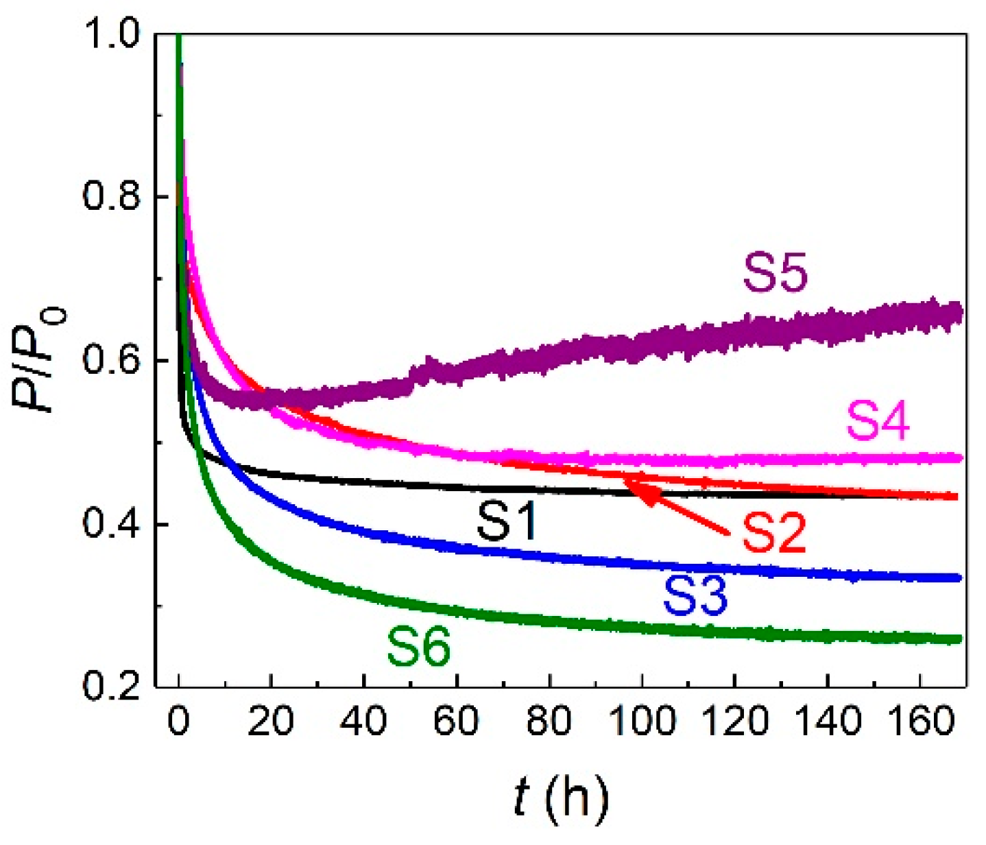
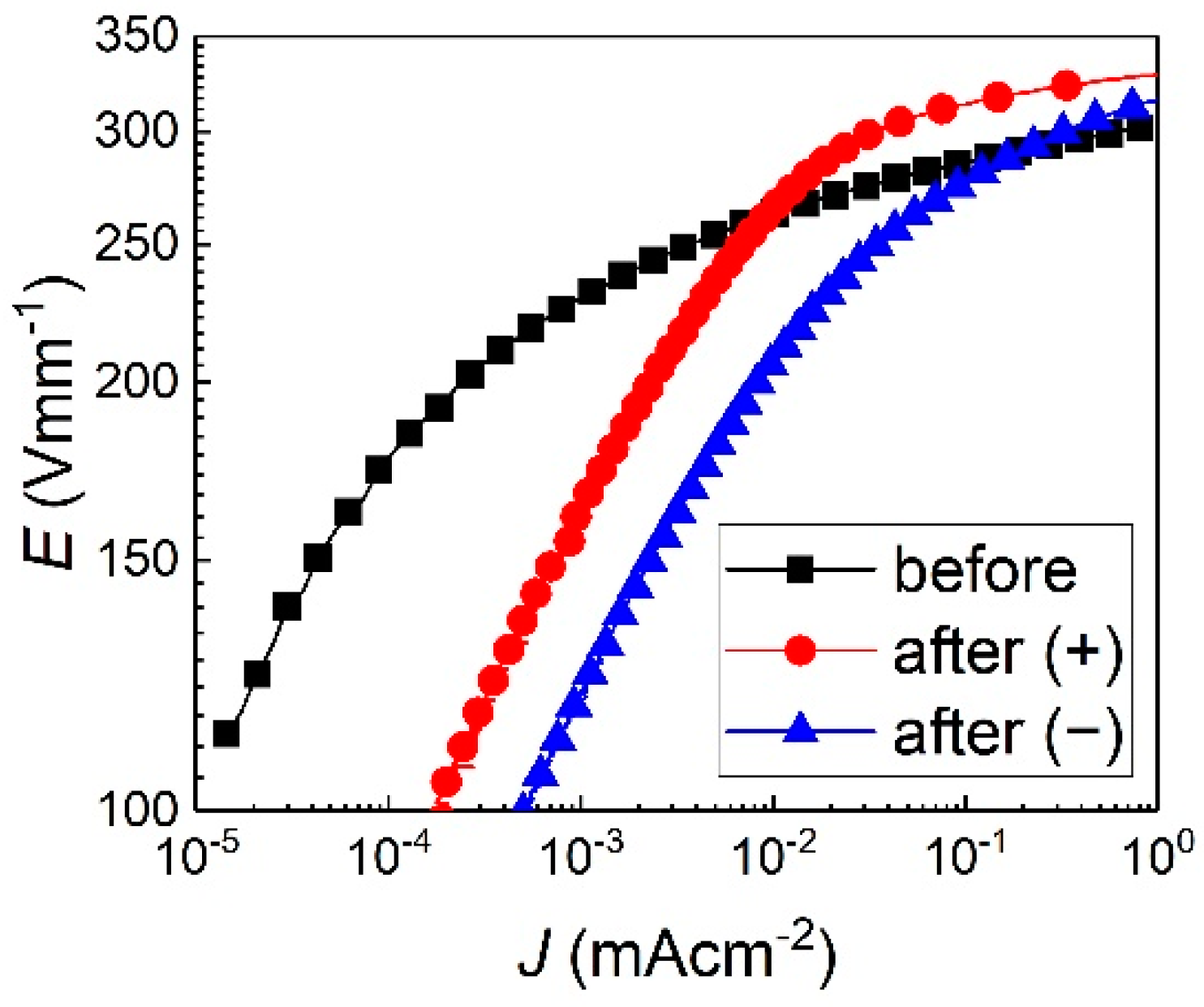
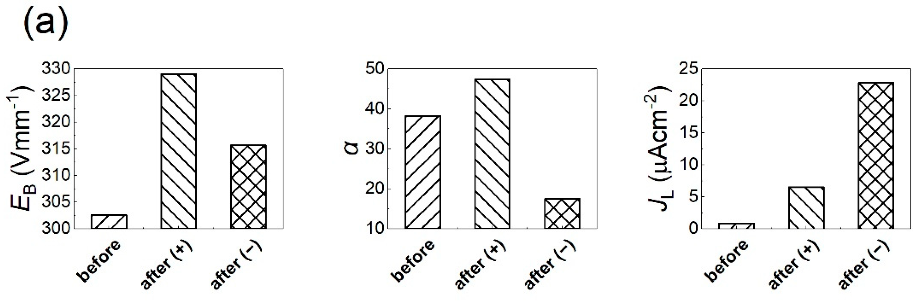
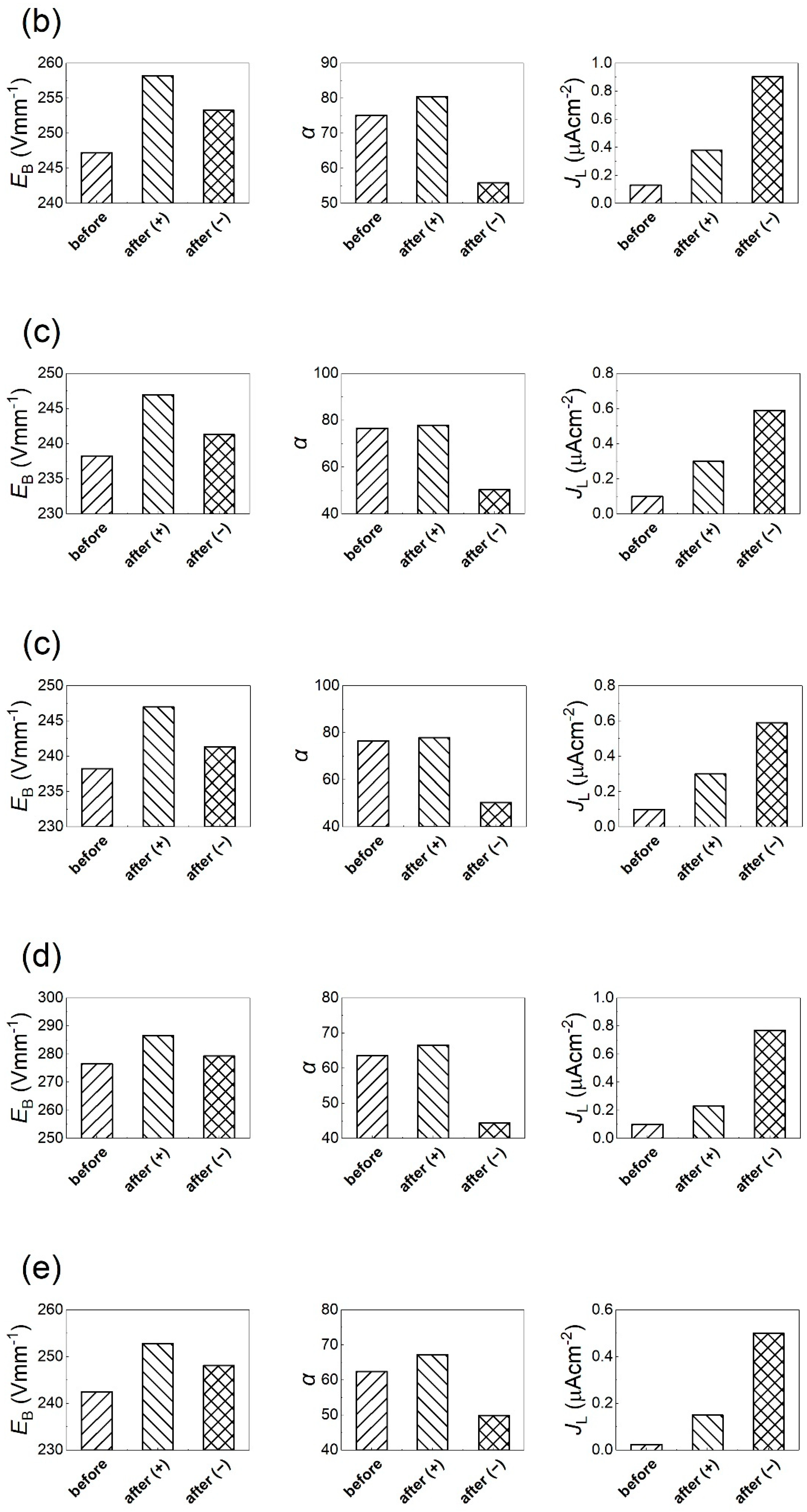
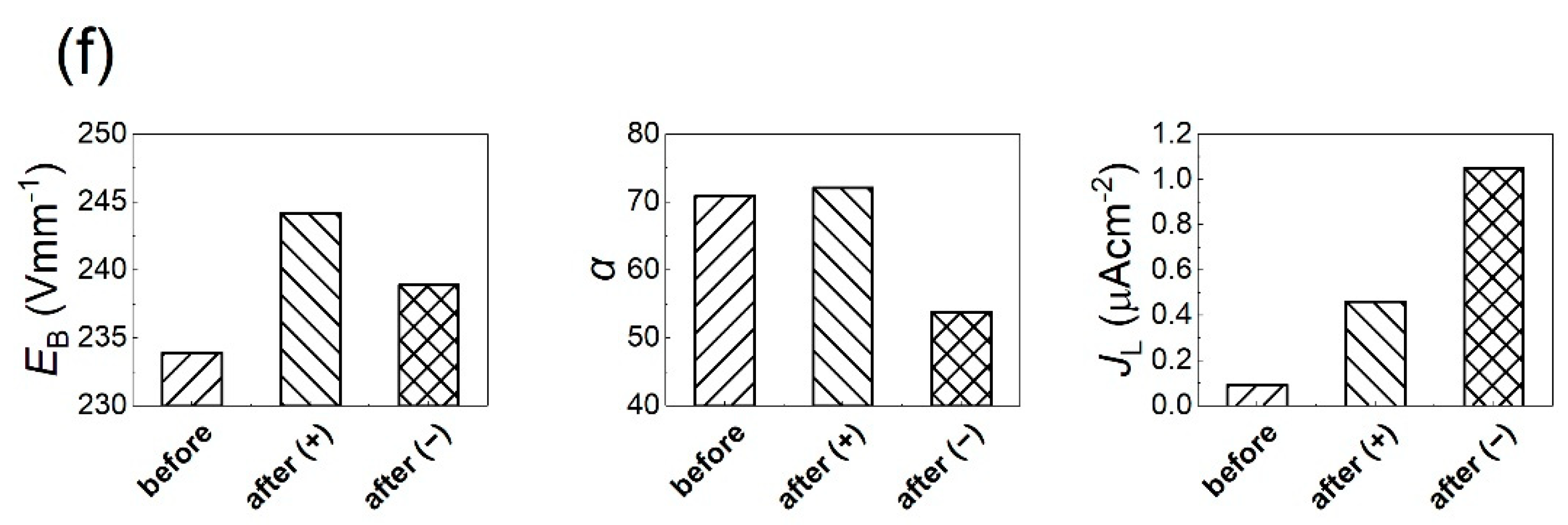
3.1. Macro Electrical Properties

Phase compositions and microstructures of all samples have been presented elsewhere [19]. α-Bi2O3 phase was detected in samples S1–S4, whereas δ-Bi2O3 phase was detected in samples S5 and S6. δ-Bi2O3 phase trended to appear in those samples with higher Co2O3 content. Spine phase Zn(Zn4/3Sb2/3)O4 was identified in S1–S3, and spine phase Co(Co4/3Sb2/3)O4 was identified in S4–S6. Average grain sizes (λ), densities (D), and porosities (H) are shown in Table 1. λ changed little with increasing Co2O3 content. D decreased at low contents, and then increased with increasing Co2O3 content. Changes of H were opposite to D. It was found that microstructures changed little after doping Co2O3.
Electrical properties of these as-sintered varistors were reported elsewhere. During DC aging, power loss (P) was continuously recorded, as shown in Figure 1. P0 is a maximum of P at the beginning of aging. P rapidly decreases in the initial time. Ion migrations were most intense when DC voltage was applied. With increasing aging time, equilibrium was established between migrations and diffusions. Thus, P gradually decreased. Approximately after 20 h, P of S5 gradually increases, whereas those of others decrease with lower rates than before. This indicates that these samples except S5 are stable under the DC aging test. As to S5, the increase of P is due to δ-Bi2O3, which is a phase of Bi2O3 with the highest conductivity of oxygen ion. During aging, adsorbed oxygen can desorb and easily escape from the varistor through δ-Bi2O3 [20]. As a result, the interface states and Schottky barrier height decrease, and P gradually increases due to increasing leakage current. Leakage current density (JL) vs. aging time (t) satisfies
J L = J L 0 + K T t ,
where JL0 is the leakage current density at t = 0; KT is the degradation rate. JL of S5 was extrapolated via Equation (1), where it would be equal to the initial value after 1489 h, with JL0 = 53.04 μA and KT = 1.45 μA·cm−2·h0.5.
As an example, J-E curves of S1 are shown in Figure 2. After DC aging, J-E curves became asymmetric in both positive direction and negative direction. Leakage currents increased in both directions, where the increase is more in the negative direction. Breakdown field also increased in both directions, where the increase is more in the positive direction. All electrical parameters of S1–S6 before and after DC aging are shown in Figure 3. Breakdown field increased more in the positive direction than the negative direction, nonlinearity increased in the positive direction, whereas it decreased in the negative direction. Leakage current density increased more in the negative direction than the positive direction. It is found that after DC aging, electrical properties degraded more seriously in the negative direction.
The nonlinear coefficient α = 1/lg(EB/EA) was calculated from the current density-electric field (J-E) curves, where EA and EB (called breakdown field) are electric fields under 0.1 mAcm−2 and 1 mAcm−2, respectively. The leakage current density (JL) was acquired at 0.75EB.

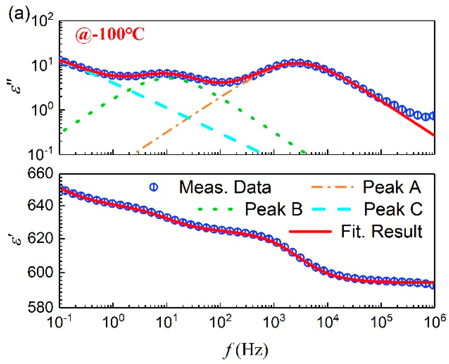
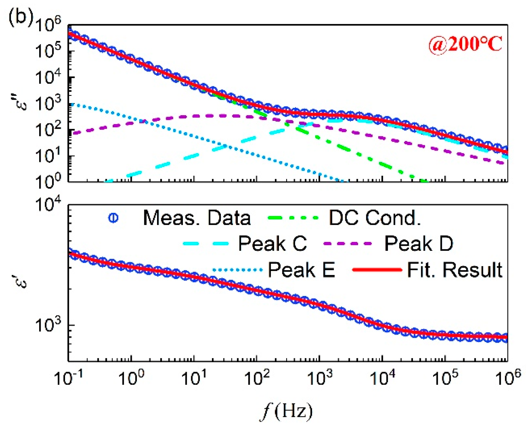
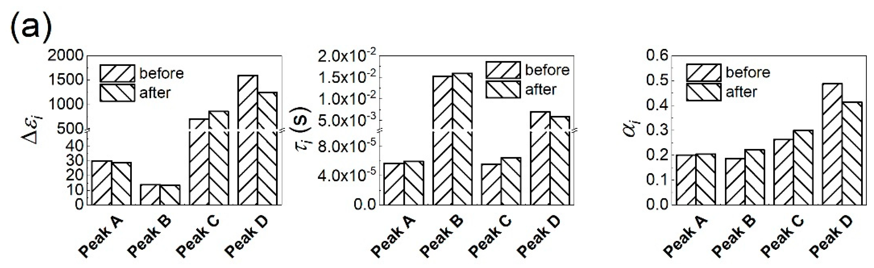
3.2. Dielectric Response

Relaxations of intrinsic point defects of Zni and oxygen vacancy (VO) can be detected at lower temperatures. Zni is the most mobile ion in ZnO varistors and plays a decisive role in aging. Relaxations of extrinsic defects respond at higher temperatures. Extrinsic defects, such as grain boundaries and intergranular phases, may be changed due to temperature rise, for example, partial melting arose from intensive heat generated in the varistors when high currents flow [21]. These defects decide the property of DSB.
As an example, dielectric responses of S1 at −100 °C and 200 °C before DC aging are presented to analyze these defects, which is shown in Figure 4. Two obvious loss peaks were manifested in ε″ spectroscopy at −100 °C in Figure 3a, while only a vague one at 200 °C in Figure 3b was detected. Frequency has effects on the electrical characteristics of varistors [22]. The reason is that DC conductivity exponentially increased at higher temperatures, which masked loss peak(s) at low frequencies. Here, frequencies lower than 10 Hz are referred to as low frequencies. Compared to Figure 2, the dielectric responses for the pristine sample had little difference. Note that some relaxation peaks were hidden by DC conductivity at high temperatures, a derivative method was applied to characterize relaxation processes [23,24]. It was found that five relaxations exist in a temperature range of −110~200 °C and a frequency range of 10−1~106 Hz. At low temperatures (−110~−60 °C), two loss peaks were detectable, which were designated as Peak A and Peak B. At high temperatures (150~200 °C), two loss peaks were also characterized that were designated as Peak C and Peak D. Because Peak E had not completely manifested in the spectra, it is not discussed in the following content.
To obtain parameters of all loss peaks and DC conductivity, Cole–Cole model was applied to fit the complex permittivity [25]:
ε = ε + σ dc j ω ε 0 + i Δ ε i 1 + ( j ω τ i ) 1 α i
In this expression, ε* = εjε″ is the complex permittivity, ε the limiting high-frequency permittivity, ω the angular frequency, σdc the dc conductivity, ε0 the vacuum permittivity, Δεi and τi the relaxation amplitude and the relaxation time for the ith relaxation, respectively, αi the shape (or relaxation time distribution) parameters.
The genetic algorithm was used to fit measurement results. For results at lower temperatures, all parameters were obtained based on ε″, and examined over ε’. For results at higher temperatures, σdc was firstly calculated via ε″ at the low frequencies. Relaxation parameters were obtained from ε’. Then, all parameters were examined by ε″. Frequency ranges of ‘steps’ in ε’ spectra or loss peaks in ε’ spectra were obtained in advance for globally optimal solutions. All parameters of loss peaks of S1–S6 before and after DC aging are shown in Figure 5. Peak A and Peak B were ascribed to the relaxation of Zni•• and VO in depletion layers [26]. After DC aging, Δεi and αi of the two peaks changed a bit. This is because of the change of defect distribution in depletions. τi of Peak A and Peak B almost did not change due to the intrinsic nature of the two defects. Peak C and Peak D were related to extrinsic defects, where Peak C was caused by inter-granular phase and Peak D is speculated due to the interface states [27,28]. Zhao et al. recently found that Peak C was related to both Bi2O3-rich phase and the spinel phase, and was therefore, due to relaxation of interface between the two phases [24]. Because of the extrinsic nature of the two defects, all parameters of Peak C and Peak D change to some extent.
DC conductivities (σdc) were obtained from σ’ spectra at 0.1 Hz, which was also calculated via dielectric responses at higher temperatures. σdc of S1–S6 at 200 °C before and after DC aging are shown in Figure 6a. After DC aging, σdc increases for every sample. As σdc was obtained from frequency-domain conductivity at the lowest measurement frequency, it reflects the property of the DSB [29,30]. Based on the Arrhenius equation, activation energies (Edc) of σdc were also calculated, as shown in Figure 6b. It is found that Edc decreases for all samples after DC aging. Therefore, the reason why σdc increases is mainly because Edc decreases, and the decrease of Edc is due to the aging of the DSB.

3.3. Discussion

DSB model was utilized to explained DC aging mechanism, as shown in Figure 7. Peak A derives from electron relaxations between donor levels of Zni and the conduction band in the depletion layers. Peak B derives from similar processes of VO. Peak C and Peak D have higher activation energies, and are related to electron emissions from different kinds of interfaces (boundaries). As leakage current density increased more in the negative direction than the positive direction, one could deduce that the forward-biased barrier height (ΦbF) decreased more and the reverse-biased barrier (ΦbR) decreased a bit during aging, i.e., ΦbF < ΦbR < Φb0. In ZnO semiconductor, Zni were too mobile to be stable at room temperature, with the migration energy about 0.57 eV [31]. Oxygen, which could be adsorbed at the grain boundary and form localized acceptor states, played a key role in forming a potential barrier [32,33].
When the DC stress was applied, the depletion width (wF) of the forward-biased barrier became narrow, while the reverse-biased barrier became wide, i.e., wF < w0 < wR. As aging time increased, metastable cations, which were mainly Zni, migrated into grains for the forward-biased barrier. As to the reverse-biased barrier, metastable cations migrated to the grain boundary, some of which recombined with part of the localized states. At the grain boundary, metastable anions migrated from the forward-biased barrier to the reverse-biased one, which replenished the interface states in the reverse-biased barrier and was postulated being Oad or its aliovalent species [34]. Finally, the barrier widths got narrower and satisfied wR < wF < w0. Therefore, all parameters of loss peaks and DC conductivity due to the change of defect structure.
The relation among the Schottky barrier height (Φb), the density of the interface states (Ni) and the donor (Nd), and the depletion width (w) satisfies the following expression [35]:
Φ b = e N d w 2 2 ε r ε 0 = e N i 2 2 ε r ε 0 N d ,
where e is the charge of an electron, εr the relative permittivity of ZnO. Hence, the previous conclusion for the deformation of the DSB was deduced. Meanwhile, the complex defects related to Peak C and Peak D also changed due to the migration of oxygen ion in the Bi2O3-rich phases. The specific defects relative to Peak D need further characterization. Besides, asymmetric conduction of ZnO varistors is also associated with nonuniform distribution of additives and grain sizes, especially due to ion redistributions after DC aging [36,37]. Conductivity, or say DSB, is a function of both voltage and temperature [38]. Ion distributions led to changes of the functions in both the positive and the negative directions. Establishing such a function is still one of the remaining challenges in the field [39].

4. Conclusions

DC aging mechanism was investigated based on Co2O3-doped ZnO varistors. During the aging process, the power loss decreased continuously except S5 with δ-Bi2O3. After DC aging, breakdown field increased more in the positive direction than the negative direction, nonlinearity increased in the positive direction, whereas it decreased in the negative direction, and leakage current density increased more in the negative direction than the positive direction.
After DC aging, parameters of four relaxations were compared with the initial value, where the amplitudes of all relaxations changed. It was deduced that the migrations of Zni and Oad changed the species of the interface states and then deformed the DSB. As a result, the forward-biased barrier height decreased more than the reverse-biased one.

Author Contributions

Conceptualization, X.Z. and H.S.; methodology, X.Z.; software, Z.H.; validation, X.Z., M.G. and Y.L.; formal analysis, Z.H.; investigation, X.Z.; resources, Z.H.; data curation, M.G.; writing—original draft preparation, M.G.; writing—review and editing, X.Z. and R.W.; visualization, Z.H.; supervision and project administration, H.S. and M.G. All authors have read and agreed to the published version of the manuscript.

Funding

This research was supported by The National Key R&D Program of China (2018YFC0809400).

Data Availability Statement

Data sharing not applicable. No new data were created or analyzed in this study. Data sharing is not applicable to this article.

Conflicts of Interest

The authors declare no conflict of interest.

References

  1. He, J.L. Metal Oxide Varistors; TsingHua University Press: Beijing, China, 2019; pp. 1–4. [Google Scholar]
  2. Kaufmann, B.; Billovits, T.; Kratzer, M.; Teichert, C.; Supancic, P. A modelling approach to describe the DC current-voltage behaviour of low-voltage zinc oxide varistors. Open Ceram. 2021, 6, 100113. [Google Scholar] [CrossRef]
  3. Tsovilis, T.E.; Topcagic, Z. DC Overload Behavior of Low-Voltage Varistor-Based Surge Protective Devices. IEEE Trans. Power Deliv. 2020, 35, 2541–2543. [Google Scholar] [CrossRef]
  4. Blatter, G.; Greuter, F. Carrier transport through grain boundaries in semiconductors. Phys. Rev. B 1986, 33, 3952–3966. [Google Scholar] [CrossRef] [PubMed]
  5. Blatter, G.; Greuter, F. Electrical breakdown at semiconductor grain boundaries. Phys. Rev. B 1986, 34, 8555–8572. [Google Scholar] [CrossRef]
  6. Gupta, T.K. Application of Zinc Oxide Varistors. J. Am. Ceram. Soc. 1990, 73, 1817–1840. [Google Scholar] [CrossRef]
  7. Gupta, T.K.; Carlson, W.G. A grain-boundary defect model for instability/stability of a ZnO varistor. J. Mater. Sci. 1985, 20, 3487–3500. [Google Scholar] [CrossRef]
  8. Eda, K.; Iga, A.; Matsuoka, M. Degradation mechanism of non-ohmic zinc oxide ceramics. J. Appl. Phys. 1980, 51, 2678–2684. [Google Scholar] [CrossRef]
  9. Gupta, T.K.; Carlson, W.G. Barrier voltage and its effect on stability of ZnO varistor. J. Appl. Phys. 1982, 53, 7401–7409. [Google Scholar] [CrossRef]
  10. Ramanachalam, M.S.; Rohatgi, A.; Schaffer, J.P.; Gupta, T.K. Characterization of ZnO varistor degradation using lifetime positron-annihilation spectroscopy. J. Appl. Phys. 1991, 69, 8380–8386. [Google Scholar] [CrossRef] [Green Version]
  11. Yang, P.; Gomez, C.A.; Andrews, S.; Sorenson, J.D.; Chen, K.S. High-voltage surge protection by a varistor-filled air gap. J. Am. Ceram. Soc. 2021, 104, 3247–3259. [Google Scholar] [CrossRef]
  12. Ohbuchi, Y.; Kawahara, T.; Okamoto, Y.; Morimoto, J. Characterization of interface states in degraded ZnO varistors. Jpn. J. Appl. Phys. 2002, 41, 190–196. [Google Scholar] [CrossRef]
  13. Takahashi, K.; Miyoshi, T.; Maeda, K. Degradation of Zinc Oxide Varistors. MRS Proc. 1981, 5, 399. [Google Scholar] [CrossRef]
  14. Ramirez, M.A.; Simoes, A.Z.; Bueno, P.R.; Márquez, M.A.; Orlandi, M.O.; Varela, J.A. Importance of oxygen atmosphere to recover the ZnO-based varistors properties. J. Mater. Sci. 2006, 41, 6221–6227. [Google Scholar] [CrossRef]
  15. Mielcarek, W.; Gubanski, A.; Paściak, G.; Prociów, K.; Warycha, J.; Wrobel, J.M. The effect of bismuth oxide polymorph forms on degradation processes in ZnO varistors. Ceram. Int. 2013, 39, 8219–8226. [Google Scholar] [CrossRef]
  16. Anderson, R.S. Lattice-vibration effects in the spectra of ZnO:Ni and ZnO:Co. Phys. Rev. 1967, 164, 398–405. [Google Scholar] [CrossRef]
  17. Kim, E.D.; Kim, C.H.; Oh, M.H. Role and effect of Co2O3 additive on the upturn characteristics of ZnO varistors. J. Appl. Phys. 1985, 58, 3231–3235. [Google Scholar] [CrossRef]
  18. Yano, Y.; Takai, Y.; Morooka, H. Interface states in ZnO varistor with Mn, Co and Cu impurities. J. Mater. Res. 1994, 9, 112–118. [Google Scholar] [CrossRef]
  19. Guo, M.; Wang, Y.; Wu, K.N.; Zhang, L.; Zhao, X.; Lin, Y.; Li, J.Y. Revisiting the effects of Co2O3 on multiscale defect structures and relevant electrical properties in ZnO varistors. High Volt. 2020, 5, 241–248. [Google Scholar] [CrossRef]
  20. Shuk, P.; Wiemhofer, H.D.; Guth, U.; Göpel, W.; Greenblatt, M. Oxide ion conducting solid electrolytes based on Bi2O3. Solid State Ion. 1996, 89, 179–196. [Google Scholar] [CrossRef]
  21. Tanaka, T.; Baba, Y.; Tsujimoto, Y.; Tsukamoto, N. FDTD Electromagnetic and Thermal Simulation of a Metal Oxide Varistor Element Considering the Temperature Dependence of Its Resistivity. Electricity 2021, 2, 158–167. [Google Scholar] [CrossRef]
  22. Staikos, E.T.; Tsovilis, T.E. Low-frequency response of low-voltage metal-oxide varistors used for telecommunication systems protection. In Proceedings of the 2020 IEEE International Conference on High Voltage Engineering and Application (ICHVE), Beijing, China, 6–10 September 2020; pp. 1–4. [Google Scholar]
  23. Huang, Y.; Wu, K.; Xing, Z.; Zhang, C.; Hu, X.; Guo, P.; Li, J.Y. Understanding the validity of impedance and modulus spectroscopy on exploring electrical heterogeneity in dielectric ceramics. J. Appl. Phys. 2019, 125, 084103. [Google Scholar] [CrossRef]
  24. Zhao, X.; Shi, W.D.; Zhang, B.Y.; Guo, M.; Shen, H.B. Relaxation peaks of ZnO varistors and their correlations with electrical properties. Jpn. J. Appl. Phys. 2021, 60, 031006. [Google Scholar] [CrossRef]
  25. Cole, K.S.; Cole, R.H. Dispersion and absorption in dielectrics I. alternating current characteristics. J. Chem. Phys. 1941, 9, 341–351. [Google Scholar] [CrossRef] [Green Version]
  26. Cheng, P.; Li, S.; Zhang, L.; Li, J.Y. Characterization of intrinsic donor defects in ZnO ceramics by dielectric spectroscopy. Appl. Phys. Lett. 2008, 93, 012902. [Google Scholar] [CrossRef]
  27. Zhao, X.; Li, J.Y.; Li, H.; Li, S.T. Intrinsic and extrinsic defect relaxation behavior of ZnO ceramics. J. Appl. Phys. 2012, 111, 6132. [Google Scholar] [CrossRef]
  28. West, A.R.; Andres-Verges, M. Impedance and Modulus Spectroscopy of ZnO Varistors. J. Electroceramics 1997, 1, 125–132. [Google Scholar] [CrossRef]
  29. Huang, Y.; Wu, K.; Tang, Z.; Xin, L.; Zhang, L.; Li, J. Investigation of electrical inhomogeneity in ZnO varistor ceramics based on electronic relaxations. Ceram. Int. 2019, 45, 1110–1114. [Google Scholar] [CrossRef]
  30. He, J.; Li, S.; Lin, J.; Zhang, L.; Feng, K.; Zhang, L.; Li, J. Reverse manipulation of intrinsic point defects in ZnO-based varistor ceramics through Zr-stabilized high ionic conducting βIII-Bi2O3 intergranular phase. J. Eur. Ceram. Soc. 2018, 38, 1614–1620. [Google Scholar] [CrossRef]
  31. Janotti, A.; Van de Walle, C.G. Fundamentals of zinc oxide as a semiconductor. Rep. Prog. Phys. 2009, 72, 126501. [Google Scholar] [CrossRef] [Green Version]
  32. Stucki, F.; Greuter, F. Key role of oxygen at zinc oxide varistor grain boundaries. Appl. Phys. Lett. 1990, 57, 446–448. [Google Scholar] [CrossRef]
  33. Bueno, P.R.; Leite, E.R.; Oliveira, M.M.; Orlandi, M.O.; Longo, E. Role of oxygen at the grain boundary of metal oxide varistors: A potential barrier formation mechanism. Appl. Phys. Lett. 2001, 79, 48–50. [Google Scholar] [CrossRef]
  34. Eda, K. Zinc oxide varistors. IEEE Electr. Insul. Mag. 1989, 5, 28–30. [Google Scholar] [CrossRef]
  35. Emtage, P.R. The physics of zinc oxide varistors. J. Appl. Phys. 1977, 48, 4372–4384. [Google Scholar] [CrossRef]
  36. Chiang, Y.; Kingery, W.D.; Levinson, L.M. Compositional changes adjacent to grain boundaries during electrical degradation of a ZnO varistor. J. Appl. Phys. 1982, 53, 1765–1768. [Google Scholar] [CrossRef]
  37. Topcagic, Z.; Tsovilis, T.E. Varistor Electrical Properties: Microstructural Effects. In Encyclopedia of Materials: Technical Ceramics and Glasses; Pomeroy, E.M., Ed.; Elsevier: Oxford, UK, 2021; pp. 254–271. [Google Scholar]
  38. Zhou, Q.; Yang, H.; Huang, X.; Wang, M.; Ren, X. Numerical modelling of MOV with Voronoi network and finite element method. IET High Volt. 2021, 1–8. [Google Scholar] [CrossRef]
  39. Greuter, F. ZnO Varistors: From Grain Boundaries to Power Applications. In Oxide Electronics; Wiley: Hoboken, NJ, USA, 2021. [Google Scholar]
Figure 1. Power losses of S1–S6 during DC aging. Aging condition: Heated at 135 °C and applied an electric field of 0.9EB for more than 160 h, where EB is the electric field when current density is 1 mAcm−2 and is called breakdown field.
Energies 14 04011 g001
Figure 2. J-E characteristics of S1 before and after DC aging.
Energies 14 04011 g002
Figure 3. Electrical parameters of S1–S6 before and after DC aging (af) S1–S6.
Energies 14 04011 g003aEnergies 14 04011 g003bEnergies 14 04011 g003c
Figure 4. Dielectric responses of S1 before DC aging (a) −100 °C (b) 200 °C.
Energies 14 04011 g004aEnergies 14 04011 g004b
Figure 5. Parameters of all loss peaks before and after DC aging (af) S1–S6.
Energies 14 04011 g005aEnergies 14 04011 g005b
Figure 6. DC conductivities (a) and their activation energies (b) of S1–S6 before and after DC aging.
Energies 14 04011 g006
Figure 7. The schematic for ion migration based on the double Schottky barrier model.
Energies 14 04011 g007
Table 1. Average grain sizes (λ), densities (D), and porosities (P) of Co2O3-doped ZnO varistors.
No.λ (μm)D (gcm−3)H (%)
S19.985.320.016
S210.275.250.018
S310.855.280.024
S410.195.230.051
S510.245.230.020
S610.715.420.021
Publisher’s Note: MDPI stays neutral with regard to jurisdictional claims in published maps and institutional affiliations.

