Article

Multi-Wire Interconnection of Busbarless Solar Cells with Embedded Electrode Sheet

1
Department of Electronic Engineering, Korea National University of Transportation, Chungju 27909, Korea
2
Department of IT Convergence, Korea National University of Transportation, Chungju 27909, Korea
*
Author to whom correspondence should be addressed.
Energies 2021, 14(13), 4035; https://doi.org/10.3390/en14134035
Submission received: 19 March 2021 / Revised: 29 June 2021 / Accepted: 29 June 2021 / Published: 4 July 2021

Abstract

:
The module technology proposed in this paper is used to fabricate a wire embedded ethyl vinyl acetate (EVA) sheet module by applying a cell/module integrated process in which the cell and wire are bonded during the lamination process. A wire-embedded EVA sheet module was fabricated using a busbarless cell and SnBiAg wire. As a result of the module characteristics corresponding to the lamination process temperature, the highest efficiency of 19.55% was observed at 170 °C. The lowest contact resistivity between the wire and the finger electrode was shown under a temperature condition of 170 °C, which was confirmed to increase the efficiency owing to an improvement of the fill factor with an excellent electrical contact.

Graphical Abstract

1. Introduction

The need for renewable energy, such as solar power, is increasing owing to environmental pollution problems caused by an increase in fossil fuel consumption. According to the International Energy Agency (IEA), solar power generation will lead the global power market and achieve the stated goal of “net zero emissions by 2050” [1,2]. Currently, the main objective of the photovoltaic (PV) industry is to lower the cost of solar power manufacturing. Among solar cell materials, silicon (Si) wafers are the most basic material used for solar cell fabrication, and the thickness of the silicon wafers is expected to decrease gradually to a thickness of approximately 150–160 µm by 2030 [3]. To reduce the cost of wafers, which is gradually decreasing, thinning is essential, and technical elements applicable to the thinning of wafers must be developed [3]. However, when the modularization process is applied using a thin solar cell, a process is used to melt the alloy coated on the ribbon at a high temperature of 300 °C to 400 °C for connecting the cell and ribbon. This causes thermal and mechanical defects in the solar cell. Thin solar cells subjected to thermal and mechanical shock for connecting the ribbon to the electrodes formed on top of the solar cell grow microcracks inside the cell through thermal cycling in the external environment. The solar cell is broken by the microcrack growth, or the upper electrode is damaged, making it difficult to properly collect the carriers [4,5,6,7]. This increases the series resistance of the solar cell, which deteriorates the long-term reliability of the solar cell module. In addition, the cooling process applied at room temperature after the high-temperature tabbing process causes a bowing phenomenon of the cell owing to the difference in the coefficient of thermal expansion (CTE) between the solar cell and ribbon [8,9,10]. In addition, to maintain a certain or greater adhesive strength when connecting the ribbon and the cell, there must be a busbar area that forms a wide silver paste on the front of the cell. Although reducing the area of the busbar while maintaining the thinness of the wafer can reduce the cost of the cell, there is a limit to reducing the thickness of the wafer or reducing the amount of paste used in the stable modularization process. Accordingly, various methods for a new module process have been proposed to minimize the negative factors affecting the cell owing to the module process and overcome the problems of the existing module process. A representative example includes a multi-busbar structure that increases the number of busbars, which is a shingled module structure, by bonding the cells using a conductive adhesive after dividing the cells with a laser [11,12]. However, a solar cell with a multi-busbar structure cannot avoid the tabbing process at high temperatures during the modularization process. Multi-busbar solar cells heated to a high temperature causes thermodynamic stress on the solder joints of solar cells owing to the mismatch of the thermal expansion coefficients of copper and silicon when cooled at room temperature. Accordingly, when thin wafers are applied to a multi-busbar module, it is not possible to improve the cell damage problem during the modularization process [13,14]. In the case of a shingled module, a division cell is used to manufacture the module, and a high voltage level can be obtained. A laser process is essential for fabricating a division cell; accordingly, laser damage inevitably occurs. Because such laser damage degrades the characteristics of the cell, it is necessary to find a process that can minimize laser damage [15,16,17]. In addition, because the interconnection of cells using shingled module technology is formed through physical contact, the various coefficients of thermal expansion of the cell and module materials such as silicon, electrode, and glass create different levels of thermo-mechanical stress in the interconnect. Accordingly, it is necessary to manufacture the module in consideration of this problem, and because the process of bonding with an additional adhesive is performed, the cost required for the process increases and the throughput is slow [18]. Accordingly, a module method to overcome the shortcomings of the currently developed module method is proposed in this paper. During the module process, the high-temperature tabbing process was eliminated, and a method for manufacturing the module using the lay-up and lamination processes was investigated. In the existing module, a ribbon was used as a wiring material to connect the cells; however, the module proposed in this paper was manufactured using a wire with a circular cross-sectional area, and a module process in which the cell and wire are bonded during the lamination process was applied. Modules manufactured using wires reduce the cell finger resistance and minimize electrical loss. It is possible to manufacture high-power modules by reducing the shadow loss owing to the re-incidence of reflected light reflected along the curved surface of the wire. In addition, this module manufacturing technology enables the modularization of solar cells without the tabbing process and can minimize the thermal damage and mechanical stress inflicted during the tabbing process. This module manufacturing method can be applied to thin wafers and to reduce the module unit cost by reducing the amount of silver in the cell, which can be a significant help in securing the productivity and economy by securing the price competitiveness of solar cell modules [19,20,21,22,23]. The cost of front and rear silver paste for busbar formation can be reduced because the wire module does not print busbars, only fingers. The costs for three and five busbar solar cells includes the cost of the silver and ribbon. The costs were approximately 17.18 and 20.23 USD, respectively, for a 72-cell module, excluding the ribbon soldering costs. The module with wire includes the cost of silver for the busbar and the costs of the ribbon, Cu, InSn, and PET. Excluding the processing cost, a module with 18 wires with a wire diameter of 300 µm and a module with 38 wires having a wire diameter of 200 µm cost 6.38 and 8.33 USD for the materials, respectively [24,25]. Modules using wires show that the cost reduction effect is extremely large, and it can be seen that the price competitiveness is greater than that of the other modules. In the module using a wire, the wire is not directly in contact with a cell with only finger electrodes, but instead is embedded in an ethyl vinyl acetate (EVA) sheet to apply an interconnection between the cell and wire. The wire was mainly coated with a SnPb solder. In this study, the lamination process was applied at a low temperature of 200 °C or less for interconnection between the busbarless cell and the wire. Accordingly, to proceed with the soldering of the wire through lamination, a low melting point solder should be used instead of the SnPb solder previously applied. Although several other research institutes have adopted this module technology, there is a difference from the module proposed herein. Among the module technologies using wires, a wiring material is fixed to the polyethylene terephthalate (PET) foil, and the foil is temporarily bonded to the cell at a temperature lower than the melting point of the solder to form a string, and the module process is conducted. SnIn solder is used as the solder, which has a melting point of 130 °C or lower, and soldering with the cell occurs during the lamination process of the module process. The use of relatively expensive solder and the inclusion of additional materials to hold the wires increases the material cost of the module [26]. In addition, there are cases in which the ribbon, which is a wiring material used in a general busbar tabbing module, is replaced with a wire to connect the cells. A string is then manufactured, and the module is created using the same methods as the general module manufacturing. In this case, a wire coated with a general SnPb solder was used, unlike the concept of using a low melting point solder. Therefore, because it is a high-temperature process, there is a risk of cell damage from thermal damage occurring during the cell tabbing process. In addition, because it proceeds through the tabbing process, a narrow busbar cell is used instead of a busbarless cell, which requires a bonding force between the cell and wire when moving after the string is created [27]. In this study, because SnBi, a low-cost solder, was used for the wire (with a melting point of <140 °C) [28] instead of SnIn (with a melting point of <125 °C) [28], the material cost of the module could be reduced by a factor of approximately 2.5. A module process is possible at low temperatures of 200 °C or lower using a low-melting-point solder coating wire of approximately 139 °C, instead of the tabbing process applied at 200 °C or higher, and thus the thermal damage of the cell can be minimized. In this paper, a method of manufacturing a module using a cell/module integrated process was proposed. This proposes a module method that interconnects a busbarless cell with only finger bars and a wire embedded in the EVA sheet. Accordingly, the paper was written by dividing the composition of the paper into two sections: busbarless cell fabrication technology and a module technology using wires are described in detail. First, finger electrodes were formed according to the Ag paste type, and the characteristics of the electrodes were analyzed using various analytical methods. The process of manufacturing a module using the busbarless cell made through this process is sequentially shown. To form an interconnection between the manufactured busbarless cell and the wire, a wire-embedded EVA sheet was first manufactured, and the effect of the lamination process temperature on the characteristics of the module with wire was then analyzed.

2. Materials and Methods

In this study, a solar cell with a passivated emitter and rear cell structure with a size of 15.675 × 15.675 cm2 was used. The experimental procedure was applied in the following order: wafer cleaning, surface texturing, POCl3 doping, passivation thin film deposition on the front and rear sides, laser ablation of the rear side, Al and Ag metallization of the front and rear sides, firing, and a solar cell analysis. The wafer was etched using KOH to remove the surface damage caused by the saw wire. After the saw damage removal process, the reflectance of the wafer was approximately 20.42% in the wavelength of 300 nm to 1100 nm. Subsequently, wafer texturing was applied using KOH and isopropyl alcohol (IPA) at a process temperature of 80 °C and a process time of 30 min. After the texturing process, the reflectance of the wafer was approximately 9.11%. An n-type emitter with 120 Ω/sq was formed on the surface-textured wafer using a furnace. The phosphorosilicate glass layer on the wafer surface was removed by immersion in a buffered oxide etch solution for 30 s. A silicon nitride (SiNx) passivation thin film with a thickness of approximately 88.8 nm was deposited on the front of the surface using plasma-enhanced chemical vapor deposition (PECVD). On the rear side, an Al2O3 thin film of approximately 11.3 nm thick was deposited using atomic layer deposition and a SiNx thin film of approximately 105 nm as a capping layer to protect the passivation thin film was deposited using plasma enhanced chemical vapor deposition (PECVD). The rear laser ablation process was conducted at intervals of 0.88 nm using a nanosecond green laser. Using a screen printing method, the rear electrode was formed using Al paste, and the front electrode was formed using two types of Ag paste. As the mesh was formated for the screen printing process, the electrode process was applied using a mesh with a structure of 90 finger lines and a finger width of 30 µm, and the screen printing process conditions were a pressure of 0.6 MPa, maximum speed, and snap off of 1.5 mm. During the firing process, an electrode was formed by fixing a maintenance temperature of 450 °C, a maintenance time of 15 s, and a peak temperature of 760 °C. After electrode formation according to the paste, the surface and cross-sectional shape of the electrode were analyzed using a field emission scanning electron microscope (FE-SEM) (Model S-4300, Hitachi, Inc., Tokyo, Japan). In addition, by calculating the resistivity value of the electrode material and the contact resistivity value between the electrode and cell, the characteristics of the two pastes were compared [29]. The current-voltage characteristics of the fabricated cell were measured using a simulator (Model PLS-300, MC science, Inc., Suwon, Korea) in AM1.5G with a power density of 100 mW/cm2.
After fabricating the busbarless cell, a wire-embedded EVA sheet was fabricated to interconnect the busbarless cell and wire. First, a wire-embedded EVA sheet was fabricated to fix the wire on the EVA sheet. A wire coated with a low-melting-point solder that reacted at the lamination process temperature of the module was used. The diameter of the wire was 0.26 mm, and the number of wires was fixed at 12. Because the solder coated on the wire is melted during the lamination process to form an interconnection between the wire and finger electrode on the front of the solar cell, a module was fabricated using a SnBiAg wire with a low melting point of 139 °C. First, to manufacture a wire-embedded EVA sheet module, the lay-up process is applied in order of glass, EVA sheet with wire, solar cell, EVA sheet with wire, and back sheet. The materials of the stacked module structure were bonded according to different process temperatures during the lamination process. The constituent materials of the module were bonded using laminator equipment. If the process conditions are not optimized, transmittance of the module is reduced by generating bubbles after the lamination process. This can reduce the power of the module because it reduces the amount of light reaching the cell. In addition, if the process temperature is unsuitable during the lamination process, the back sheet surrounding the rear surface of the module is not firmly bonded, and a partial separation phenomenon occurs, which significantly affects the life and durability of the module. Therefore, the lamination process temperature was varied to optimize the module process. The lamination process conditions included a pumping time of 40 s, Upper-Vacuum time of 60 s, Upper-Vacuum 01 time of 50 s, Upper-Vacuum02 time of 50 s, Upper-Vacuum03 time of 50 s, and Lower-Vacuum time of 60 s. Figure 1 shows the profile of the lamination process. To evaluate the characteristics of the module manufactured using the wire-embedded EVA sheet, the power was measured using a solar simulator. The module power was measured under the standard conditions of AM1.5G (100 mW/cm2). In the case of a short-circuit current (Isc), which is one of the characteristics that determines the power of the module, the solar cell with the lowest Isc determines the overall Isc of the solar panel in a series connection of solar cells [30,31]. In addition, for the fill factor, the average value of the cell input to the module is matched. For this reason, when cells with large efficiency deviations are modularized, the power of the module is reduced. Therefore, the power of the module can be increased only when the module is manufactured after selecting similar cells through cell sorting before manufacturing the module. In this study, after measuring the efficiency of the cell before manufacturing the module, the module process was carried out with a cell having a similar efficiency.

3. Results

The experiment was divided into two parts. First, a finger-line electrode formation for a busbarless cell formation was applied. Then, an EVA sheet using a low-melting-point solder-coated wire was fabricated for the wire-embedded EVA sheet module, and the module process was conducted using a laminator.

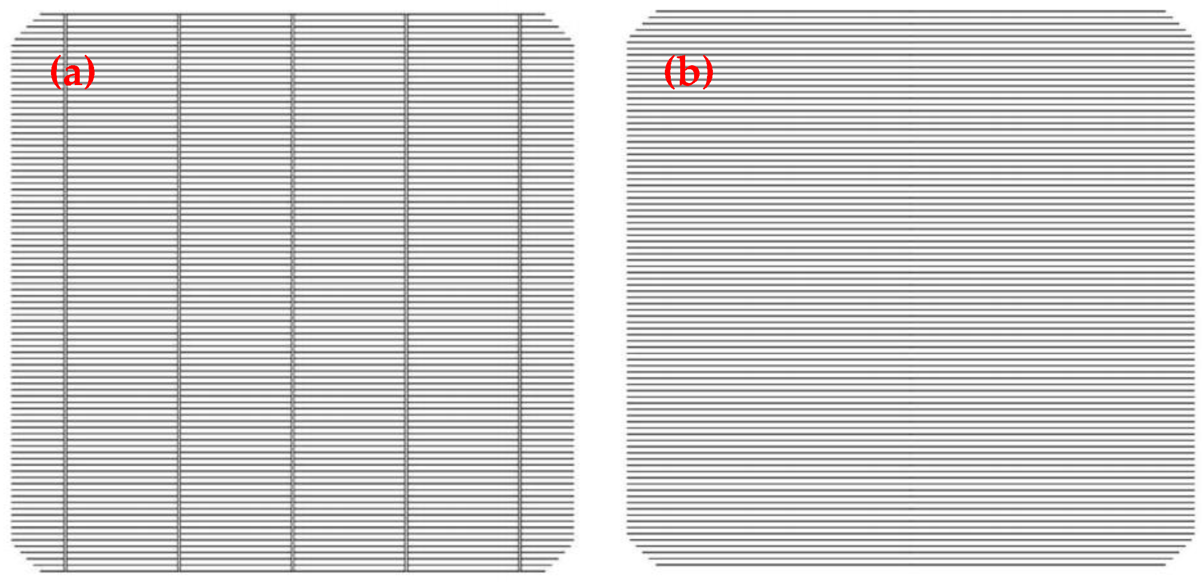
3.1. Finger Electrode Formation for Busbarless Cell

The finger electrode formation process that can apply busbarless cell/module integration technology is an extremely important factor. The formation process for the front and rear electrodes of a solar cell using screen printing was conducted. An electrical analysis was conducted after forming an electrode on a p-type Si solar cell with a thickness of approximately 200 µm, a resistivity of approximately 1.5 Ω·cm, and a sheet resistance of approximately 120 Ω/sq for an n-type emitter formed using POCl3. The rear electrode was formed using Al paste, and the front electrode was formed using two types of Ag paste. First, to analyze the effect of the Ag paste type on the electrode formation before the electrode formation process, two types of Ag paste were analyzed, and the electrode formation process was then conducted. Table 1 shows the viscosities of pastes A and B.
Prior to the electrode process, the viscosity characteristics of pastes A and B and the change in viscosity of the polymer solution by an external force called thixotropy (T.I.) were observed. The viscosity characteristics were measured at 20 rpm to 100 rpm, and the T.I. was calculated as 5/50 rpm viscosity. It can be seen that the viscosity of pastes A and B gradually decreased as the measurement speed increased. The viscosity characteristic of the paste is an extremely important factor for paste comparison analysis because it maintains the uniform size and height of the electrode after forming the electrode. Because screen printing properties are strongly influenced by the viscosity of the paste, it is necessary to compare the printing properties after adjusting the viscosity of the paste to the same level. Comparing the viscosity characteristics of the paste, it was found that paste B showed a slightly higher value than paste A. Thus, the characteristics of the cell electrode can be compared and analyzed based on the resistivity of the paste or the electrode formation process, rather than the paste characteristics owing to the viscosity, and structural and electrical analyses of the paste were conducted. First, the resistivity of the electrode material of pastes A and B, and the contact resistance between the electrode and the cell the transmission line method (TLM), were calculated, and the characteristics of the pastes were compared. Figure 2 shows the method used to measure the resistivity of the electrode [32] and the contact resistivity between the electrode and cell [33,34]. Here, ρ c is contact resistivity, L is length of electrode, and R T is total resistance.
First, a sample was prepared to measure the resistivity of the electrode material, and the line resistance was then measured. In this case, to measure the resistivity of the electrode more accurately, as many finger electrodes with the same thickness and width as possible should be formed [29]. After measuring the line resistance according to the distance, the cross-sectional area and width of the electrode were measured. The formula for calculating the resistivity of the electrode is as follows:
ρ L i n e   =   R L i n e × A W
In the above equation, ρ L i n e is the resistivity of electrode, and R L i n e is the line resistance of electrode. W is width of electrode, and A is the cross sectional area of electrode.
Figure 3 shows a graph of the line resistance of the electrode according to the paste type. As a result of measuring the line resistance of the electrode after forming an electrode according to the paste type, the line resistance of the paste B showed a much smaller numerical value. As a result, the resistivities of the pastes A and B were 1.2 × 10⁻⁴ Ω cm and 3.5 × 10⁻⁶ Ω cm, respectively. This can be explained through the data obtained by measuring the shape of the electrode using a 3D microscope, as shown in Figure 4. It can be seen that the electrode formed using paste A is non-uniform when compared with paste B after the electrode formation process. If the line resistance of an electrode with a non-uniform height and width is measured, the resistance may be measured as inaccurate. Therefore, because explaining the cause of the improved efficiency by analyzing the paste based on the resistivity is insufficient, the cause of the efficiency improvement according to the paste types was analyzed by comparing the contact resistivity using the TLM.
The contact resistivity between the electrode and cell can be calculated using a TLM analysis. After printing an Ag paste on a silicon substrate using screen printing, drying, and firing processes, the contact resistivity with the electrode was measured through TLM measurements. The contact resistivity was calculated using the dark state current–voltage (Dark IV), and when measuring the total resistance (RT) in the dark state current–voltage, the voltage range is −1.00 to 1.00 V. The I–V line was then plotted, and the RT value was obtained through Ohm’s law. In the graph of the RT value and the distance between the electrodes, the intercept values of the x- and y-axes are the transfer length (2LT) and 2Rc values, respectively. From this, the Rc and LT values were obtained, and the contact resistivity ( ρ c) was obtained using the theoretical equation ρ c = RcLTW. The LT value represents the distance through which most of the current flows when a current flows from the silicon to the electrode or from the electrode to the silicon [35].
To accurately calculate the contact resistivity of the electrode, the cross-sectional area and width of the electrode were observed using SEM images, as shown in Figure 5. The line width of the electrodes formed using pastes A and B showed a similar value of approximately 43 µm, with aspect ratios of 0.35 and 0.41, respectively. Accordingly, it was confirmed that the electrode formed using paste B had a higher aspect ratio. It can be predicted that the efficiency will be improved owing to the higher aspect ratio during the electrode formation process as well as the resistance characteristics of the paste material.
Figure 6 shows the contact resistivity values of the electrodes when Ag electrodes were formed using different types of paste. First, the contact resistivity value of paste A was approximately twice as high as that of paste B, and through this, it was found that the electrical properties were excellent when paste B was used. To analyze the cause of the decrease in contact resistivity, the wafer with the electrode was dipped in RCA-1 and an hydrogen fluoride (HF) solution for 30 min, and cross-sectional and surface images were then analyzed through FE-SEM.
Figure 7 shows SEM images of the glass layer according to the type of paste. The thickness of the glass layer after electrode formation has a significant influence on the collection of electrons. First, when the cross-sectional image was observed, Ag particles were present in empty spaces such as holes in the glass layer, and the SEM image shows the surface and cross-sectional state of the wafer after removing the Ag particles through solution treatment [36]. Before solution treatment, Ag particles gather to form a path through which electrons can flow across the entire surface. The thicker the glass layer, the more difficult it is to form a current path, unless the Ag particles are as large as the thickness of the glass layer. Accordingly, to form a contact area of an electrode capable of collecting more electrons, the thickness of the glass layer must be thin. In addition, when the surface image was observed after removing the Ag particles, it can be seen that the dense empty spaces such as pores indicate that the Ag particles were densely formed before removing the Ag particles. As indicated, the passage through which the electrons can be collected is better formed. When comparing the shape of the electrode formed using pastes A and B, paste A has a non-uniform empty space, which means that the electrode that contacts the emitter before solution treatment is not properly formed. In addition, small particles are distributed in the glass part, which indicates that Ag particles are not removed despite the solution treatment, which cannot form a current path because Ag particles are trapped in the glass layer. Therefore, it was confirmed that when paste A rather than paste B was used, the contact area between the emitter and the electrode was not smooth, and the contact resistivity increased.
Figure 8 shows the screen printing mesh pattern according to the number of busbars. The number and width of finger electrodes are the same, but there is a difference between those with or without of busbars. Busbarless cells are formed by screen printing, and busbarless cells cannot be measured with a general simulator jig. Accordingly, the formation conditions of the finger electrodes for busbarless cells were the same as those of the 5bb electrode formation process. Figure 9 shows the electrical properties after forming electrodes using pastes A and B. The characteristics results of cell were obtained from 5bb cell due to the lack of a proper system to measure busbarless cells, it is assumed that the results of 0bb cell are the same, since the only difference is metal shading percentage.
The value of open-circuit voltage for pastes A and B was similar, showing 0.665 V and 0.67 V, respectively. However, the values of short-circuit current and fill factor value showed a slight difference. It was confirmed that the value of fill factor showed a difference due to the influence of the contact specific resistance, as shown in Figure 6. When paste A was used, the efficiency was approximately 20.5%, whereas when paste B was used, the efficiency was approximately 21.6%. It was confirmed that the efficiency was improved by approximately 1%, and these reasons could be expected in three ways, as predicted through the paste characteristic analysis. As the first, the paste has excellent resistance and electrical properties, and as the second, the contact resistivity is improved by the excellent shape of the electrode formed by the optimized screen printing process, resulting in an improved efficiency [36]. To increase the contact resistivity characteristics, methods such as an improvement of the paste material component, change in electrode structure such as a local electrode structure including electrode process optimization, and application of an electrode pattern with a fine line width may be used. As the third, the efficiency is also affected by the short-circuit current value, as well as fill factor value. This can be explained through Figure 7. From the above experimental results, it was confirmed that the thinner the glass layer, the more advantageous it is to form a current path to collect electrons. When the surface image of the electrode was observed after removing the Ag particles, the electrode formed using paste B had more dense Ag particles. Through this, it can be seen that the current path through which electrons can collect is better formed, and the current value is measured higher. Based on the results obtained through various analysis, the upper finger electrode of the busbarless cell was fabricated through paste B, and the module process was performed using a busbarless cell in which were electrodes with excellent characteristics.

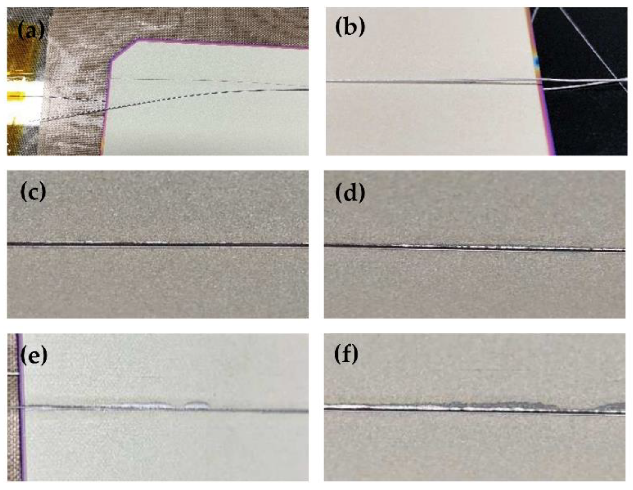
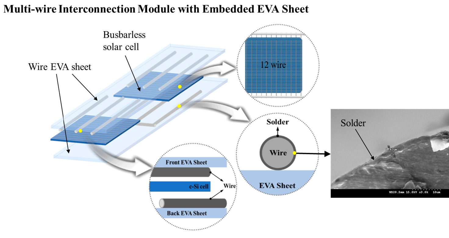
3.2. Wire Embedded EVA Sheet Module Formation

There are many types of wires used to manufacture modules with low-melting-point solder-coated wires. In this case, if a solder with a melting point is too high, the solder coated on the wire cannot melt during lamination. Therefore, it is necessary to use a solder with a low melting point that can melt at the lamination temperature. In this study, a module was fabricated using wires coated with a Sn40.5Bi58Ag1.5 solder. The module was manufactured according to the following procedure to manufacture a module using a low-melting-point solder-coated wire: First, the EVA sheet was manufactured in advance, using a wire before the module was manufactured. After placing the PET film on the EVA sheet, the low-melting-point solder-coated wires were arranged according to a fixed number of 12, and the EVA was then melted and fixed through an iron. Subsequently, the glass, upper EVA sheet, busbarless solar cell, and lower EVA sheet were mounted on the laminator for the lamination process. Finally, after the back sheet was stacked in the module structure, the lamination process was initiated. To manufacture a high-power module using a wire-embedded EVA sheet, the low-melting-point solder coated on the wire must be melted through the lamination process to make contact with the finger electrode of the cell. Accordingly, the lamination melting point temperature of the wire must be analyzed. In this experiment, the structural and electrical characteristics of the wire used to fabricate a wire-embedded EVA sheet module were analyzed, and based on the results of the characteristic analysis, a method was applied to improve the power of the module manufactured using the wire. When manufacturing a module, the solder coated on the wire is not directly affected by the laminator temperature, owing to the module components such as glass, an EVA sheet, and a back sheet. Therefore, a sample was manufactured using the same module material as when manufacturing the module, and a peel-off test of the wire was conducted according to the lamination process temperature. A wire coated with SnBiAg solder was used, and the lamination process temperature was varied from 130 °C to 190 °C. Figure 10 shows the peel off test results based on the adhesive strength according to the lamination process temperature, and Figure 11 shows the image of the SnBiAg-solder-coated wire bonded according to the process temperature after the lamination process. Although the melting point of the SnBiAg solder was 139 °C, it was confirmed that the adhesive strength was measured at 150 °C. The numerical representation of the adhesive strength represents the relative adhesive strength of the wire, and exhibits a value of 250 gf or more on average at a temperature of 150 °C. As can be seen from Figure 10, the wire did not melt at 140 °C or lower, and thus the adhesive properties could not be confirmed. At 150 °C, there was a difference in the adhesive strength between the center and side of the wire, which was found to be a low process temperature sufficiently melting the solder coated on the wire. In addition, as the temperature increased, the solder coated on the wire melted further, and the molten solder could be clearly observed at 190 °C. Therefore, when manufacturing a module using a SnBiAg solder-coated wire through an adhesion strength experiment according to the process temperature, the lamination process temperature must be applied at 150 °C or higher. This increases the probability that the solder coated on the wire will be sufficiently melted and adhere to the finger line electrode with a thin line width of 30 μm; thus, a high-power module can be expected.
Through the above experiment, after conducting a mechanical strength test of the wire in contact with the finger electrode, it was possible to confirm the lowest lamination process temperature at which the wire could be sufficiently melted. In addition, to analyze the electrical characteristics formed by melting the low-melting-point solder coated on the wire when contacting the finger electrode and the wire, a sample was prepared, as shown in Figure 12. When the contact resistivity was measured using a solar cell, because it was affected by the current flowing through the emitter, the sample was fabricated by depositing a SiNx thin film as an insulator on a p-type silicon wafer. A finger electrode was formed under the same conditions as in the electrode process formed on a silicon wafer, and a low-melting-point solder-coated wire was placed in contact with the finger electrode formed by varying the temperature from 150 °C to 200 °C. To analyze the electrical characteristics of the sample, the contact resistivity was measured using a probe station and a source meter (Model 2110, Keithley Instruments, Inc., Cleveland, OH, USA).
The values of Rtotal and Rc can be expressed using Equations (2) and (3). The contact resistivity ( ρ c ) can be expressed through Equation (4), and the contact resistivity was calculated, as shown in Equation (5). R t o t a l is total resistance, R w i r e is resistance of wire, and R f i n g e r is resistance of finger electrode. R c is contact resistance between finger electrode and wire, and A is the contact area between the wire and the finger. The contact area was derived through microscopic measurement, and the line width of the finger electrode and the contact width of the wire and the finger electrode were calculated.
R t o t a l = 2 R w i r e + R f i n g e r + 2 R c
R c = R t o t a l 2 R w i r e R f i n g e r 2
ρ c = R c A
ρ c = R t o t a l 2 R w i r e R f i n g e r 2 · A
To measure the contact resistivity between the wire and sample, the resistances of the wire and finger electrode were measured. To proceed with the electrical characteristic analysis, a wire with a diameter of 0.26 mm and a length of 10 cm was used. At this time, it was confirmed that the resistivity of the wire calculated based on its line resistance was approximately 1.69 × 10⁻⁶ Ω · cm. The Ag paste resistance of the finger electrode was confirmed based on the above experiment, and exhibited a value of 3.5 × 10⁻⁶ Ω · cm. Table 2 shows the structural and electrical characteristics of the wire and finger electrodes used for the electrical analysis.
Figure 13 shows the contact resistivity characteristics between the low-melting-point solder-coated wire and the sample according to the lamination process temperature calculated by considering the resistance values of the wire and finger electrodes. The process temperature was increased from 150 °C to 200 °C. The contact resistivity tended to decrease rapidly from a temperature of 160 °C or higher, and the contact resistivity was similarly measured at temperatures of 160 °C or higher. This means that, if the lamination process is applied at a temperature of 160 °C or higher, the low-melting-point solder coated on the wire will sufficiently melt, and thus an excellent electrical contact between the wire and the finger electrode can be formed. In this manner, the series resistance is lowered, thereby improving the module characteristics, such as the fill factor and efficiency.
To analyze the effect of the process temperature on the module characteristics during the lamination process, the module was manufactured by varying the lamination process temperature from 150 °C to 200 °C. All the cells used to manufacture the module had the same structure, and the lamination process conditions were all applied under the same conditions. At this time, the wire diameter was 0.26 mm and the number of wires was 12.
Figure 14 shows the characteristics of the manufactured module according to the process temperature. The open-circuit voltage and short-circuit current characteristics of the module did not show significant differences under any conditions. However, the fill factor showed a similar pattern as the variation in the range of efficiency. Accordingly, it was found that the fill factor significantly influences the efficiency. Although the fill factor value was not significantly different under the process temperature conditions of 150 °C and 180 °C, it was confirmed that the contact resistivity values were significantly different under the temperature conditions of 150 °C and 180 °C, as shown in Figure 13. This can be explained through Figure 11 and Figure 12. On the side of the cell, the contact resistivity value was measured by interconnecting the wire and the finger electrode through the lamination process, and the FF value was measured after the modularization process was performed. As shown in Figure 11, it can be seen that the solder coated on the wire has melted traces in the process temperature condition of 150 °C, but it is not completely melted. Accordingly, the contact resistivity value was measured to be high. On the other hand, it was confirmed that the solder coated on the wire was completely melted under the process temperature condition of 180 °C. In the module process, the wire is laid up with materials such as glass and EVA sheet to be interconnected with the cell, and the module is completed through the lamination process. As a result of module characteristic analysis, it was confirmed that the solder coated on the wire at a temperature of 150 °C does not melt and only contacts the finger electrodes because the lamination process temperature has not reached the temperature at which the solder can be melted. However, at a process temperature of 180 °C, the wire is not in simple contact with the finger electrode, but the solder coated on the wire completely melts, thereby further promoting the formation of interconnection between the wire and the electrode. Accordingly, a difference in the contact resistivity value was clearly observed at the process temperatures of 180 °C and 150 °C, though FF value showed similar results. As a result, a module manufactured at a process temperature of 180 °C showed a higher efficiency value of approximately 0.3% than a module manufactured at a process temperature of 150 °C. This value represents the absolute difference between the efficiency values. As can be seen from Figure 15, the reason for the difference in contact resistivity and fill factor according to the lamination process temperature is shown in a schematic diagram. When the wires are interconnected to the finger electrodes according to the lamination process temperature, the solder coated on the wires does not melt under low temperature conditions. Accordingly, there are few contact points between the finger electrodes and the wires. On the other hand, under high temperature conditions, the solder coated on the wire melts and the contact point between the finger electrode and the wire increases. This indicates that, as the contact point between the electrode and the wire increased, the shading loss increased and the current density was decreased. Accordingly, the module manufactured at 150 °C showed higher current density characteristics than the module manufactured at 180 °C. However, it was confirmed that the module manufactured at 150 °C shows a low efficiency of 18.328%. This is because the module manufactured at 150 °C was manufactured only by simple contact due to the pressure received from the glass. On the other hand, the module manufactured at 180 °C showed excellent contact resistivity, as the interconnection between wire and finger electrode was further promoted despite the slight decrease in short-circuit current characteristics. As a result, it was confirmed that the fill factor was improved.
Table 3 shows the module characteristics according to lamination process temperature. As a result of comparing the module efficiency manufactured under a temperature condition of 150 °C or higher, the highest efficiency of 19.55% was observed at a temperature of 170 °C [37]. This can be expected to improve the efficiency owing to the increase in the fill factor. Through the electrical characteristic analysis between the wire and finger electrode, the contact resistivity was the lowest at 170 °C, which resulted in an excellent electrical contact. Thus, it was determined that the fill factor was improved, and thus the efficiency increased. Under a temperature of 200 °C, although the solder coated on the wire was sufficiently melted, it showed a low efficiency because the solder coated on the wire is excessively melted and the molten solder area extends not only to the portion in contact with the finger electrode, but also to the portion where the electrode is not deposited, that is, the SiNx passivation thin film layer. As a result, the shadow loss increases owing to the extended solder area and short-circuit current characteristics of the solar cell, resulting in a reduced efficiency. The reduction in efficiency at process temperature of 200 °C can be explained by a decrease in fill factor as well as a decrease in short-circuit current. At a process temperature of 190 °C or higher, the solder coated on the wire melts excessively and the solder contacts the edge of the cell, affecting the part of p-n junction. Accordingly, it was confirmed that the fill factor decreased due to decreased shunt resistance value. It is considered that the efficiency decreased due to the decrease in short-circuit current caused by the shadow loss and the decrease in the fill factor by the shunt resistance decrease in the high temperature process condition. As a result, through the module efficiency analysis according to the variation in the process temperature, it was confirmed that the module can obtain the highest efficiency under a process temperature of 170 °C.

4. Conclusions

A wire-embedded EVA sheet module was fabricated by applying a cell/module integrated process. The wire-embedded EVA sheet module was fabricated using a busbarless cell and SnBiAg solder-coated wire. Although a SnBiAg wire has a low melting point of 139 °C, the temperature directly applied to the wire is much lower because of the material of the module that is mounted in the laminator equipment. Therefore, the characteristics of the module according to the lamination process temperature were analyzed. When the module was fabricated by varying the lamination process temperature, the open-circuit voltage and short-circuit current characteristics of the module did not show a significant difference under all conditions. However, the fill factor showed a pattern similar to the varying range in efficiency. The efficiency was found to be significantly influenced by the fill factor. As a result of comparing the module efficiency manufactured under a temperature condition of 150 °C or higher, the highest efficiency of 19.55% was observed at a temperature of 170 °C. This can be expected to improve the efficiency owing to an increase in the fill factor. The lowest contact resistivity at 170 °C determined through an electrical characteristic analysis between the wire and finger electrode was found, and an excellent electrical contact was formed; in addition, it was determined that the fill factor was improved, and thus the efficiency was increased.

Author Contributions

J.E.P. was the main author, carried out the experiments, and analyzed the data. W.S.C. reviewed and analyzed the data and formatting. D.G.L. conceived the ideas of the analyzed results. All authors participated in the discussion of the results, reviewed the manuscript, and provided input for editing. All authors have read and agreed to the published version of the manuscript.

Funding

This work was supported by the Korea Electric Power Corporation. (Grant no. R17XA05-1), the Korea Institute of Energy Technology Evaluation and Planning (KETEP) and the Ministry of Trade, Industry & Energy (MOTIE) of Korea (no. 20193020010650).

Data Availability Statement

Not applicable.

Conflicts of Interest

The authors declare no conflict of interest.

References

  1. Statistical Review of Wolrd Energy, 69th ed.; bp Statistical Review of World Energy 2020: London, UK, 2020; p. 65.
  2. Report. Statistical Review of World Energy Full Report. 2016, pp. 2–19. Available online: http://oilproduction.net/files/especial-BP/bp-statistical-review-of-world-energy-2016-full-report.pdf (accessed on 12 March 2021).
  3. Fischer, M.; Hanwha, Q.; CELLS GmbH; Woodhouse, M. The National Renewable Energy Laboratory, Susanne Herritsch, VDMA Photovoltaic Equipment, Jutta Trube. In International Technology Roadmap for Photovoltaic 11th; VDMA Photovoltaic Equipment, Lyoner Str.18; VDMA: Frankfurt am Main, Germany, 2020; pp. 1–83. [Google Scholar]
  4. Theunisen, L.; Wilems, B.; Burke, J.; Tonini, D.; Galiazo, M.; Henkens, A. Electrically conductive adhesives as cell interconnection material in shingled module technology. AIP Conf. Proc. 2018, 1999, 080003-1–08003-6. [Google Scholar]
  5. Pletzer, T.M.; van Mölken, J.I.; Rißland, S.; Breitenstein, O.; Knoch, J. Influence of cracks on the local current-voltage parameters of silicon solar cells. Prog. Photovolt. Res. Appl. 2013, 23, 428–436. [Google Scholar] [CrossRef]
  6. Meyer, E.L.; van Dyk, E.E. Assessing the Reliability and Degradation of Photovoltaic Module Performance Parameters. IEEE Trans. Reliab. 2004, 53, 83–92. [Google Scholar] [CrossRef]
  7. Kaushika, N.; Rai, A. An investigation of mismatch losses in solar photovoltaic cell networks. Energy 2007, 32, 755–759. [Google Scholar] [CrossRef]
  8. Hasan, M.K.; Sasaki, K. Thermal deformation analysis of tabbed solar cells using solder alloy and conductive film. J. Mech. Sci. Technol. 2016, 30, 3085–3095. [Google Scholar] [CrossRef] [Green Version]
  9. Lai, C.; Su, C.-H.; Lin, K. Analysis of the thermal stress and warpage induced by soldering in monocrystalline silicon cells. Appl. Therm. Eng. 2013, 55, 7–16. [Google Scholar] [CrossRef]
  10. Yoon, P.; Baek, T.; Chung, H.; Song, H.; Shin, S. Numerical simulation of bowing phenomenon in ultra-thin crystalline silicon solar cells, Solar Energy. Sol. Energy 2014, 105, 705–714. [Google Scholar] [CrossRef]
  11. Kunz, O.; Evans, R.J.; Juhl, M.K.; Trupke, T. Understanding partial shading effects in shingled PV modules. Sol. Energy 2020, 202, 420–428. [Google Scholar] [CrossRef]
  12. Park, J.; Oh, W.; Park, H.; Jeong, C.; Choi, B.; Lee, J. Analysis of solar cells interconnected by electrically conductive adhesives for high-density photovoltaic modules. Appl. Surf. Sci. 2019, 484, 732–739. [Google Scholar] [CrossRef]
  13. Rendler, L.C.; Kraft, A.; Ebert, C.; Eitner, U.; Wiese, S. Mechanical Stress in Solar Cells with Multi Busbar Interconnection—Parameter Study by FEM Simulation. In Proceedings of the 2016 17th International Conference on Thermal, Mechanical and Multi-Physics Simulation and Experiments in Microelectronics and Microsystems (EuroSimE), Montpellier, France, 18–20 April 2016; pp. 1–5. [Google Scholar]
  14. Rendler, L.C.; Kraft, A.; Ebert, C.; Wiese, S.; Eitner, U. Investigation of Thermomechanical Stress in Solar Cells with Multi Busbar Interconnection by Finite Element Modeling. In Proceedings of the 32nd European Photovoltaic Solar Energy Conference and Exhibition, München, Germany, 20–24 June 2016; pp. 94–98. [Google Scholar]
  15. Eiternick, S.; Kaufmann, K.; Schneider, J.; Turek, M. Loss analysis for laser separated solar cells. Energy Procedia 2014, 55, 326–330. [Google Scholar] [CrossRef]
  16. Korzeniewska, E.; Tomczyk, M.; Pietrzak, Ł.; Hadžiselimoví, M.; Štumberger, B.; Sredenšek, K.; Seme, S. Efficiency of Laser-Shaped Photovoltaic Cells. Energies 2020, 13, 4747. [Google Scholar] [CrossRef]
  17. Xia, L.; Chen, J.; Liao, K.; Huang, L.; Li, Q.; Luo, X. Influence of laser cutting conditions on electrical characteristics of half-size bifacial silicon solar cells. Mater. Sci. Semicond. Process. 2020, 105, 104747. [Google Scholar] [CrossRef]
  18. Chunduri, S.K.; Schmela, M. Advanced Solar Module Technology; TaiyangNews UG: Munich, Germany, 2018; pp. 1–55. [Google Scholar]
  19. Soederstroem, T.; Papet, P.; Ufheil, J. Smart wire connection technology. In Proceedings of the 28th European Photovoltaic Solar Energy Conference, Paris, France, 30 September–4 October 2013; pp. 495–499. [Google Scholar]
  20. Silveira, A.; Barbin, S.E.; Kretly, L.C. Using TDR-Time Domain Reflectometry Measurements to Compare Ribbon Busbar versus Wire Busbar Connections in Polycrystalline Solar Cells: The Signature Approach. In Proceedings of the IEEE-APS Topical Conference on Antennas and Propagation in Wireless Communications (APWC), Cartagena, Colombia, 10–14 September 2018; pp. 954–956. [Google Scholar]
  21. Faes, A.; Despeisse, M.; Levrat, J.; Champliaud, J.; Badel, N.; Kiaee, M.; Söderström, T.; Yao, Y.; Grischke, R.; Gragert, M.; et al. SmartWire solar cell interconnection technology. In Proceedings of the 29th European Photovoltaic Solar Energy Conference, Amsterdam, The Netherlands, 22–26 September 2014; pp. 2555–2561. [Google Scholar]
  22. Schulte-Huxel, H.; Blankemeyer, S.; Morlier, A.; Brendel, R.; Köntges, M. Interconnect-shingling: Maximizing the active module area with conventional module processes. Sol. Energy Mater. Sol. Cells 2019, 200, 109991. [Google Scholar] [CrossRef]
  23. Yao, Y.; Papet, P.; Hermans, J.; Soderstrom, T.; Mehlich, H.; Konig, M.; Richter, A. Module integration of solar cells with diverse metallization schemes enabled by SmartWire Connection Technology. In Proceedings of the IEEE 42nd Photovoltaic Specialist Conference (PVSC), New Orleans, LA, USA, 14–19 June 2015; pp. 1–5. [Google Scholar]
  24. Faes, A.; Lachowicz, A.; Bettinelli, A.; Ribeyron, P.; Lerat, J.; Munoz, D.; Geissbühler, J.; Li, H.; Ballif, C.; Despeisse, M. Metallization and interconnection for high-efficiency bifacial silicon heterojunction solar cells and modules. Met. Interconnect. 2018, 41, 65–76. [Google Scholar]
  25. Walter, J.; Tranitz, M.; Volk, M.; Ebert, C.; Eitner, U. Multi-wire interconnection of busbar-free solar cells. Energy Procedia 2014, 55, 380–388. [Google Scholar] [CrossRef]
  26. Shakhray, I.; Abramov, A.; Abolmasov, S.; Terukova, E.; Andronikov, D. Heterojunction technology: The path to high efficiency in mass production. Photovolt. Int. Pap. Thin Film 2015, 43, 52–61. [Google Scholar]
  27. Rendler, L.C.; Walter, J.; Geipel, T.; Volk, M.; Ebert, C.; Eitner, U. Modelling and verification of mechanical stress induced by soldering of wires for multi busbar interconnection. In Proceedings of the 31st European Photovoltaic Solar Energy Conference and Exhibition, Hamburg, Germany, 14–18 September 2015; p. 84. [Google Scholar]
  28. Bastow, E. Solder Families and How They Work. Adv. Mater. Process. 2003, 161, 26–29. [Google Scholar]
  29. Kitaoka, Y.; Tono, T.; Yoshimoto, S.; Hirahara, T.; Hasegawa, S.; Ohba, T. Direct detection of grain boundary scattering in damascene Cu wires by nanoscale four-point probe resistance measurements. Appl. Phys. Lett. 2009, 95, 052110. [Google Scholar] [CrossRef]
  30. Srri, B.; Tiwari, S. Sorting Of Solar Cells. Int. J. Adv. Res. Electron. Commun. Eng. 2018, 7, 777–779. [Google Scholar]
  31. Yusufoglua, U.A.; Min, B.; Pletzer, T.M.; van Mölken, J.I.; Kurz, H. Simulation and analysis of PV module performance by innovative sorting methods. Energy Procedia 2012, 27, 685–690. [Google Scholar] [CrossRef] [Green Version]
  32. Singh, Y. Electrical Resistivity Measurements: A Review. Int. J. Mod. Phys. Conf. Ser. 2013, 22, 745–756. [Google Scholar] [CrossRef]
  33. Meier, D.L.; Schroder, D.K. Contact resistance: Its measurement and relative importance to power loss in a solar cell. IEEE Trans. Electron. Devices 1984, 31, 647–653. [Google Scholar] [CrossRef]
  34. Reeves, G.K.; Harrison, H.B. Obtaining the specific contact resistance from transmission line model measurements. IEEE Electron. Device Lett. 1982, 3, 111–113. [Google Scholar] [CrossRef]
  35. Vinod, P.N. Specific contact resistance measurements of the screen-printed Ag thick film contacts in the silicon solar cells by three-point probe methodology and TLM method. Mater. Electron. 2011, 22, 1248–1257. [Google Scholar] [CrossRef]
  36. Vinod, P.N. SEM and specific contact resistance analysis of screen-printed Ag contacts formed by fire-through process on the shallow emitters of silicon solar cell. Mater. Electron. 2009, 20, 1026–1032. [Google Scholar] [CrossRef]
  37. Shahid, J.; Mittag, M.; Heinrich, M. A multidimensional optimization approach to improve module efficiency, power and costs. In Proceedings of the 35th European PV Solar Energy Conference and Exhibition, Brussels, Belgium, 24–28 September 2018. [Google Scholar]
Figure 1. Lamination process profile.
Energies 14 04035 g001
Figure 2. Method used to measure the resistivity for the electrode and the contact resistivity between the electrode and cell: (a) Resistivity for the electrode and (b) Contact resistivity between the electrode and the cell.
Energies 14 04035 g002
Figure 3. Line resistance of electrode according to paste types.
Energies 14 04035 g003
Figure 4. 3D microscope images of electrode according to paste types: (a) A and (b) B.
Energies 14 04035 g004
Figure 5. SEM images (left, width; right, height) of finger electrode formed according to paste types: (a) A and (b) B.
Energies 14 04035 g005
Figure 6. Contact resistivity of electrode according to paste types.
Energies 14 04035 g006
Figure 7. SEM images of glass layer according to paste types: (a) A and (b) B.
Energies 14 04035 g007
Figure 8. Screen printing mesh pattern according to the number of busbars: (a) 5bb cell, (b) Busbarless cell (0bb).
Energies 14 04035 g008
Figure 9. Cell characteristics after electrode formation process according to paste types: (a) Open-circuit voltage, (b) Short-circuit voltage, (c) Fill factor, and (d) Efficiency.
Energies 14 04035 g009
Figure 10. Peel-off test result according to lamination process temperature.
Energies 14 04035 g010
Figure 11. Wire adhesion strength test image according to lamination process temperature: (a) 140 °C, (b) 150 °C, (c) 160 °C, (d) 170 °C, (e) 180 °C, and (f) 190 °C.
Energies 14 04035 g011
Figure 12. Measurement method of electrical properties of low-melting-point solder-coated wire: (a) Sample, (b) Finger electrode, (c) Wire, (d) Glass.
Energies 14 04035 g012
Figure 13. Contact resistivity of low-melting-point solder-coated wire according to lamination process temperature.
Energies 14 04035 g013
Figure 14. Module characteristics according to lamination process temperature.
Energies 14 04035 g014
Figure 15. Schematic diagram of interconnection between low-melting-point solder-coated wire and busbarless cell according to lamination process temperature.
Energies 14 04035 g015
Table 1. Viscosity of paste types.
Paste AViscosity2.7 × 105 cps (20 rpm)
1.4 × 10⁵ cps (50 rpm)
8.7 × 10⁴ cps (100 rpm)
T.I.
Value (5/50 rpm)
1.94
Paste BViscosity1.9 × 105 cps (20 rpm)
1.3 × 10⁵ cps (50 rpm)
7.8 × 10⁵ cps (100 rpm)
T.I. Value
(5/50 rpm)
0.46
Table 2. Structural and electrical characteristics of wire and finger electrodes.
CharacteristicsValue
Wire length10 cm
Wire diameter0.26 mm
Wire resistivity1.69 × 10−6 Ω · cm
Finger resistivity3.5 × 10−6 Ω · cm
Finger width43 μm
Table 3. Module characteristics according to lamination process temperature.
Temperature (°C) V o c ( V ) J s c ( mA / cm 2 ) FF (%) E f f ( % ) R s   ( Ω )
1500.66741.31966.46818.3280.015
1600.66741.51467.48418.6880.014
1700.66742.29969.28819.5530.012
1800.66641.28767.77618.6330.015
1900.66541.26165.36217.9270.015
2000.66540.17159.33815.8550.017
Publisher’s Note: MDPI stays neutral with regard to jurisdictional claims in published maps and institutional affiliations.

