
DC Solid-State Circuit Breakers with Two-Winding Coupled Inductor for DC Microgrid

Abstract
:1. Introduction
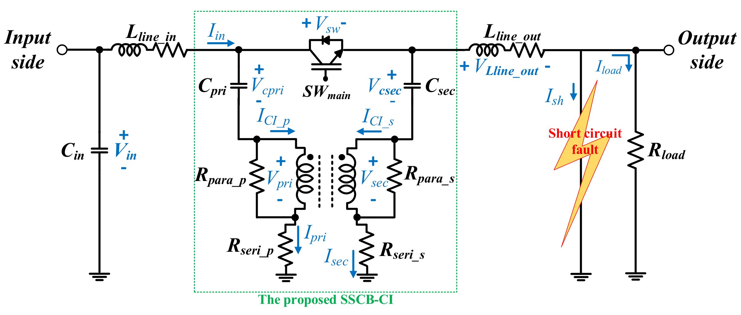
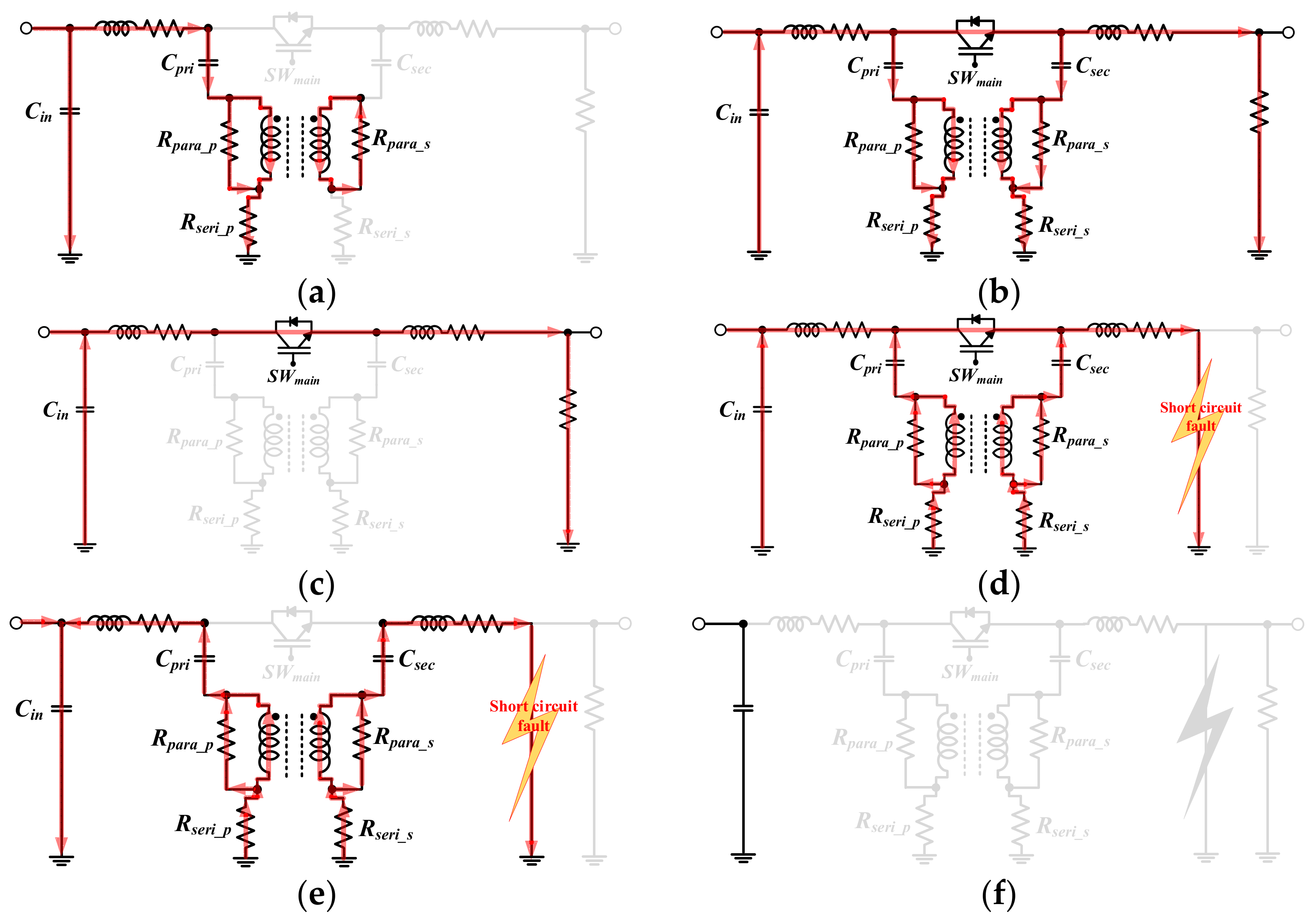
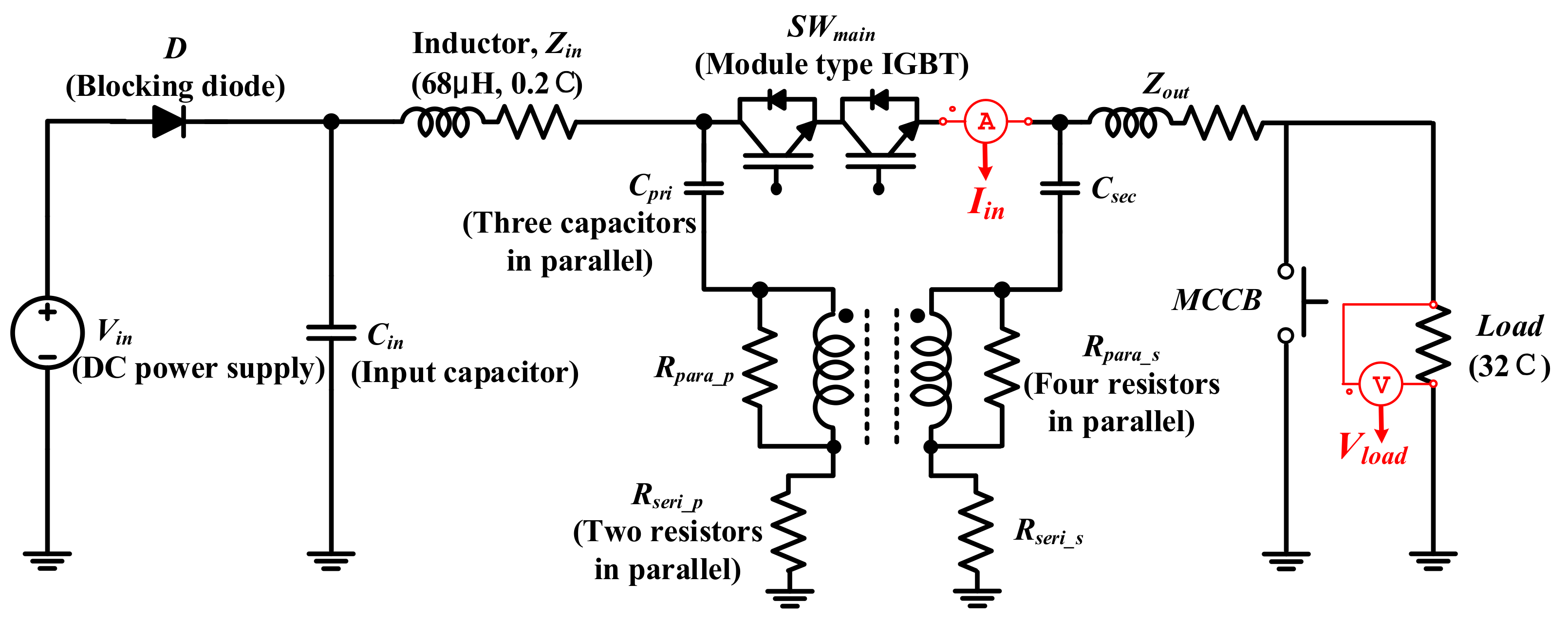
2. Operation of the SSCB-CI
- (i)
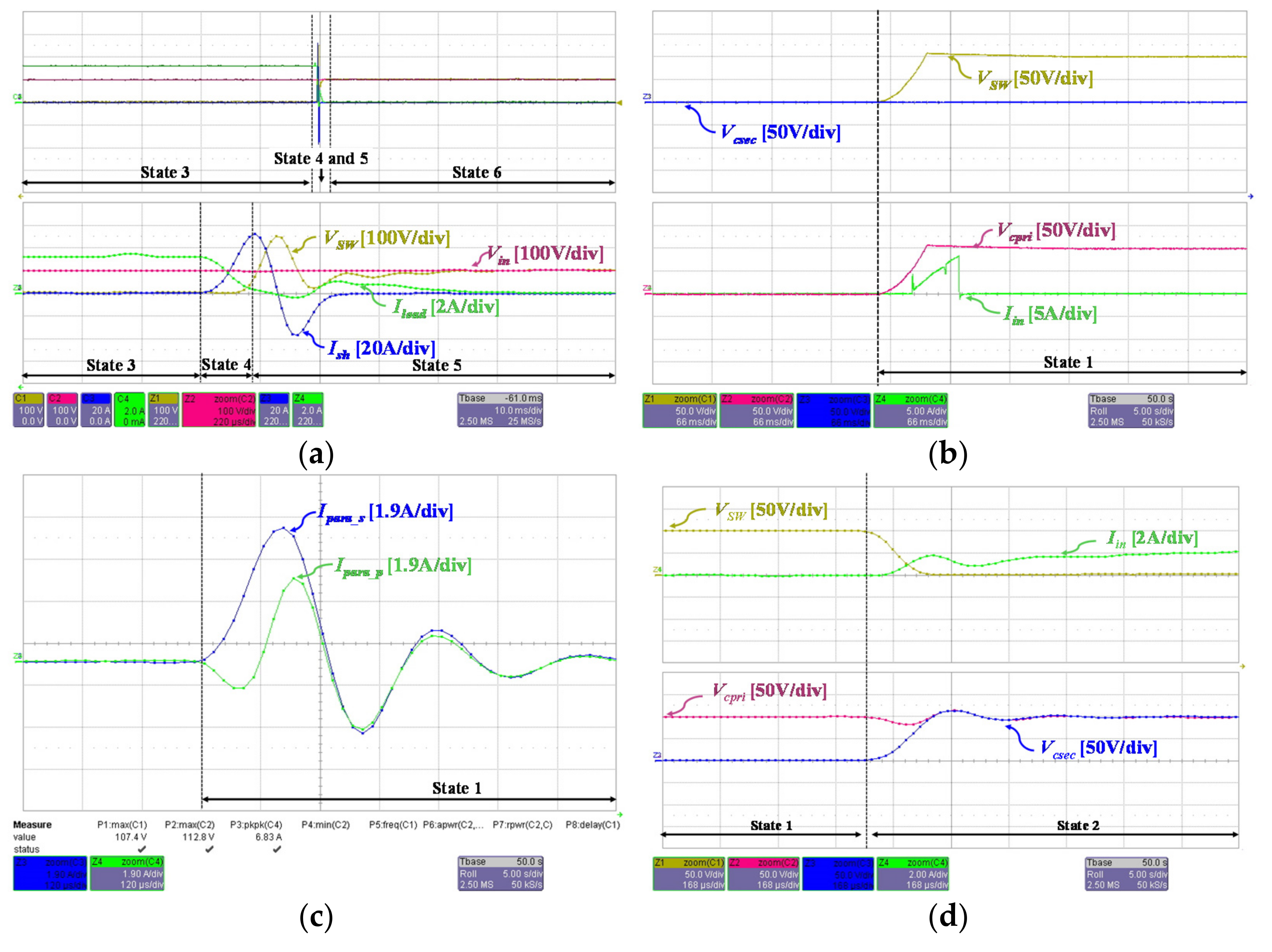
- State 1: Pre-charge of commutation capacitor in the primary side (t0~t1)This state is occurred to charge Cpri under steady state of the DC microgrid. In Figure 2a, this state means the initial state of the SSCB-CI, and occurs when SWmain turns off at the normality of the input voltage Vin. During this state, Cpri is charged. The initial condition of Ish, Ipri, and Iin can be expressed as Equation (1).The voltages across capacitors VCpri is similar to Vin. After charging, the primary winding current ICI_P is removed, thereby eliminating any unexpected power losses by Rpara_p and Rseri_p in the stationary state.
- (ii)
- State 2: Pre-charge of commutation capacitor in the secondary side (t1~t2)After State 1, if SWmain turns on, Csec is charged, and it can be shown as in Figure 2b. The current flow in the secondary winding is similar as that in State 1, but Cpri is discharged temporarily because of the voltage fluctuation of the secondary winding voltage Vpri. After that, Cpri is charged again as Vin, where the input current and the input voltage can be expressed as Equations (2) and (3), respectively.where L is the self-inductance of each winding, Lp and Ls, where two self-inductances are considered herein to have equal inductance. That is, the CI is modeled as an ideal transformer, which has a turns ratio of 1:1, the same magnetizing inductor, and the same leakage inductor. In addition, the winding resistance is neglected for ease of understanding. Therefore,
- (iii)
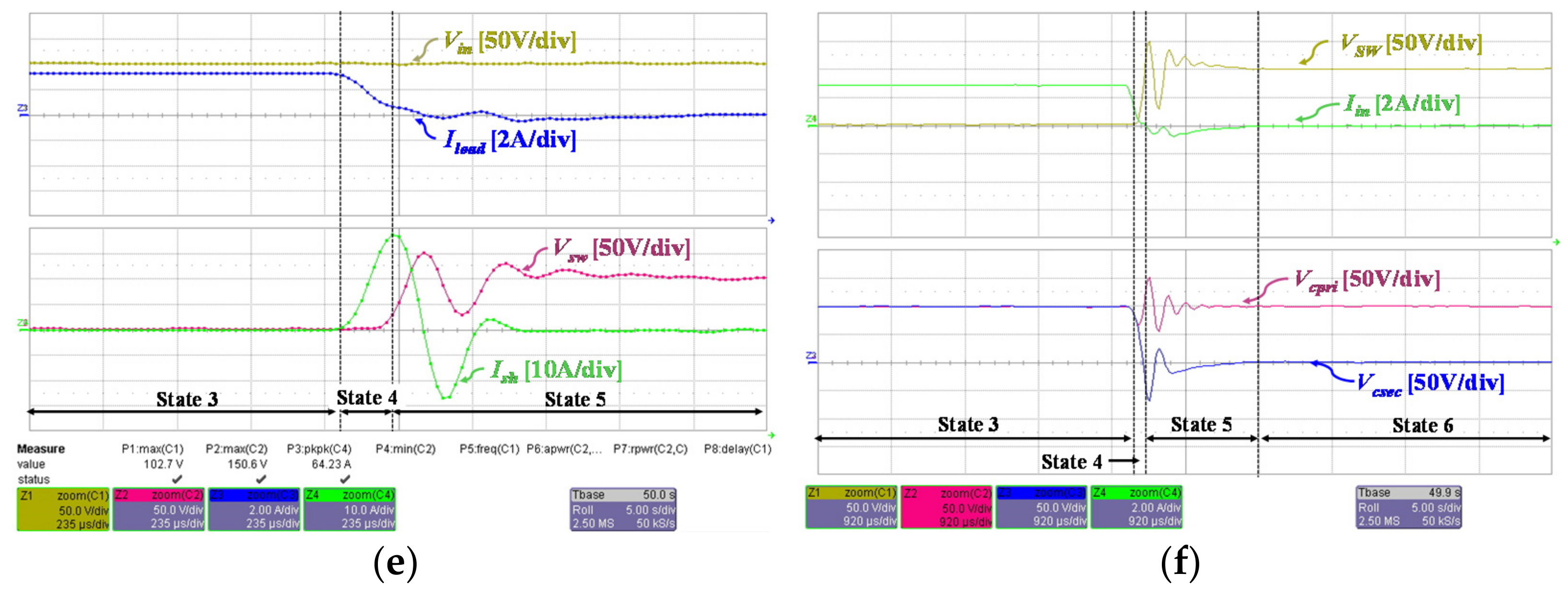
- State 3: Stationary (t2~t3)This state means the interval between the capacitor charging state and time interval state, as shown in Figure 2c. SWmain is continuously turned on and the input current Iin flows to the load as Iload.Until a line-to-ground short-circuit fault, the SSCB-CI stays. At this state, ICP_P and ICP_S are removed as zero. In addition, the voltages across Cpri and Csec are regarded as equal to Vin.
- (iv)
- State 4: Time interval (t3~t4)Figure 2d indicates the voltage and current rise after the line-to-ground fault. In this state, the instantaneous fault current is generated because of the short-circuit fault at the load side. However, SWmain is not turned off immediately because of the short interval time from the trip delay and fault detection. Therefore, Iin and Ish are increased simultaneously. During this state, Ish can be expressed as Equation (6). In this equation, only inductance, Lline_in and Lline_out, as the line impedance are considered for an easy analysis.where Rline_in and Rine_out are the mean resistor components of each line impedance.
- (v)
- State 5: Block and commutating fault current (t4~t5)Figure 2e shows the commutating fault current flow. When the detected level of Iin is exceeded, this state occurs, and consequently SWmain is turned off. The fault current in State 5 can be assumed using Equation (7).where α and ωd mean the damping ratio and the resonant frequency by Lline_out and Csec, respectively. Consequentially, the larger the resistance value, the larger the damping ratio.After Ish reaches the peak level, SWmain is stressed to more than Vin, namely a blocking voltage. Where, Vsw at State 5 can be expressed as follows:After Ish reaches the peak level, SWmain is stressed as VSW_max, namely a blocking voltage, as Equations (10) and (11).After Ish reaches the peak level, SWmain is stressed as VSW_max, namely a blocking voltage. During this state, Ish flows through the secondary winding by discharging the capacitor energy of Cpri and Csec. As Csec discharges, VCpri and VCsec oscillate momentary for a few micro seconds, and then become stable. As a result, an induced energy to the primary winding decreases Ish. As a result of the series resonance configuration, the current waveforms in the SSCB-CI circuit are produced as a sinusoidal current that has zero crossing points and is damped by Rseri_p and Rseri_s.
- (vi)
- State 6: Protection (t5~t6)The final state is the isolation of the load to Vin after a short-circuit fault. After blocking the fault current, Csec is discharged. During this state, fault restoration should be adequately achieved. After fault restoration, the operation state is returned to State 1.
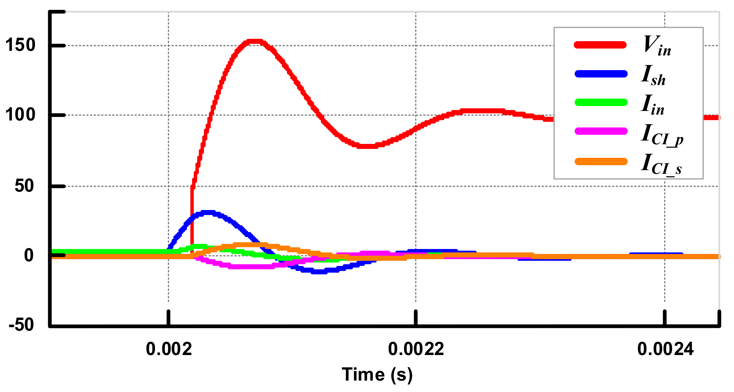
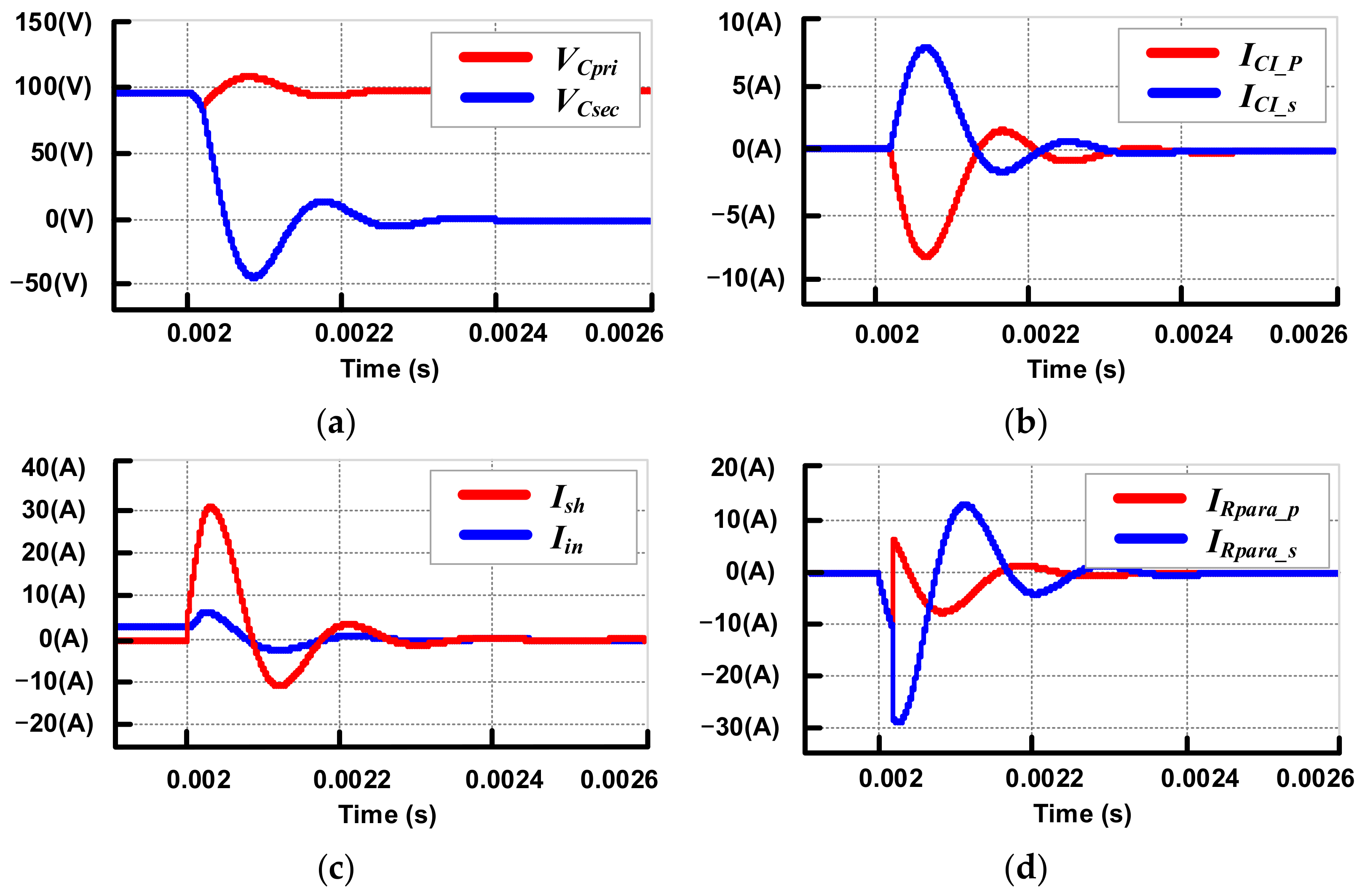
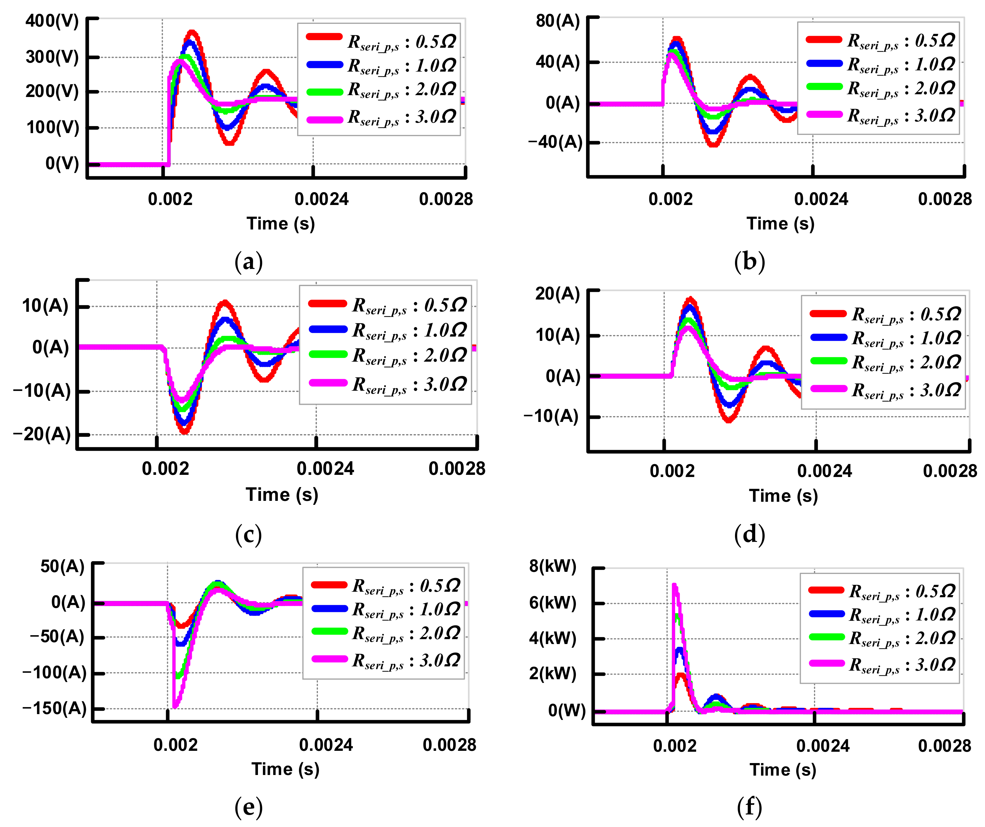
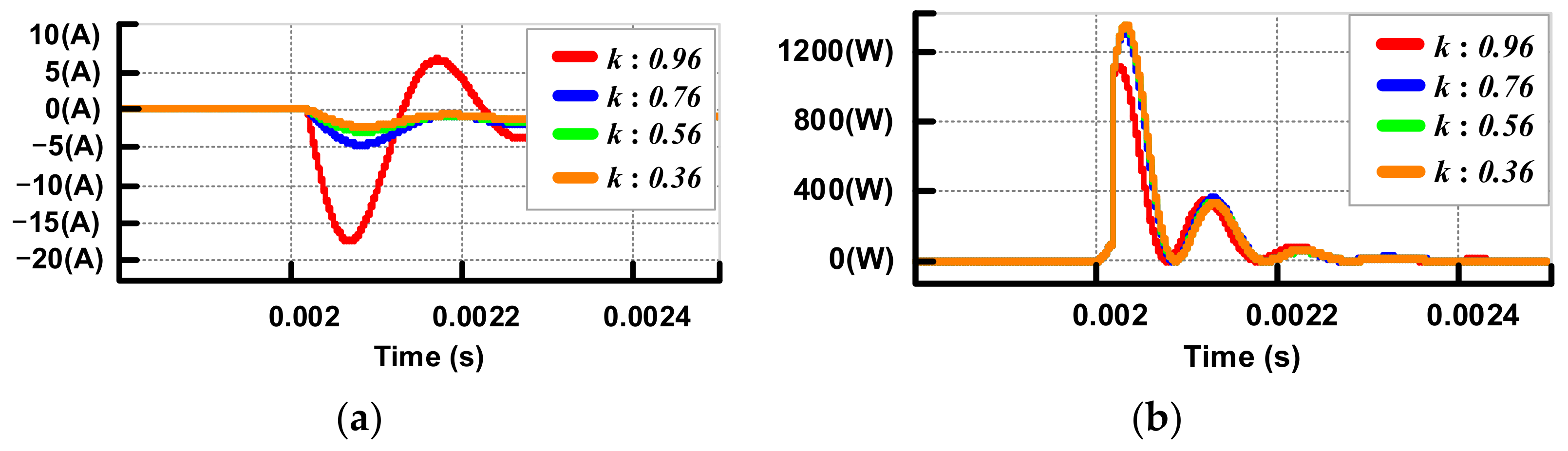
3. Simulation Results
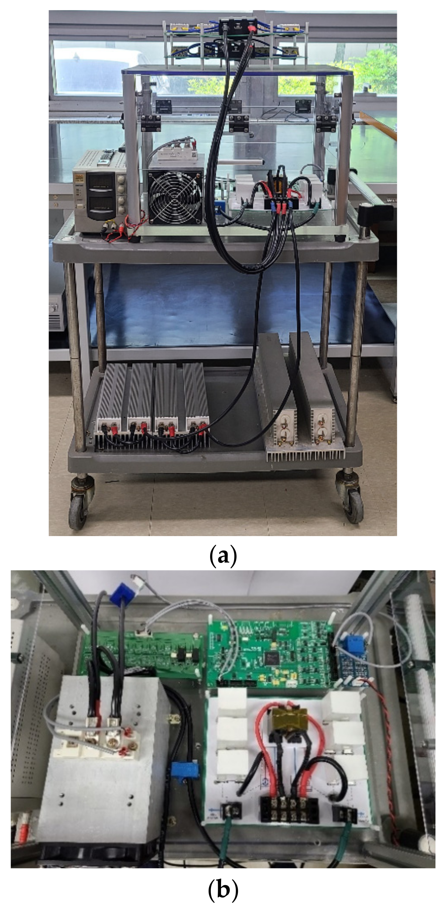
4. Experimental Results
5. Conclusions
Author Contributions
Funding
Institutional Review Board Statement
Informed Consent Statement
Data Availability Statement
Acknowledgments
Conflicts of Interest
References
- Miao, Z.; Sabui, G.; Roshandeh, A.M.; Shen, Z.J. Design and Analysis of DC Solid-State Circuit Breakers Using SiC JFETs. IEEE J. Emerg. Sel. Top. Power Electron. 2016, 4, 863–873. [Google Scholar] [CrossRef]
- Chae, S.; Park, J.; Oh, S. Series DC Arc Fault Detection Algorithm for DC Microgrids Using Relative Magnitude Comparison. IEEE J. Emerg. Sel. Top. Power Electron. 2016, 4, 1270–1278. [Google Scholar] [CrossRef]
- Tapia, L.; Baraia-Etxaburu, I.; Valera, J.J.; Sanchez-Ruiz, A.; Abad, G. Design of a Solid-State Circuit Breaker for a DC Grid-Based Vessel Power System. Electronics 2019, 8, 953. [Google Scholar] [CrossRef] [Green Version]
- Xu, X.; Chen, W.; Tao, H.; Zhou, Q.; Li, Z.; Zhang, B. Design and Experimental Verification of an Efficient SSCB Based on CS-MCT. IEEE Trans. Power Electron. 2020, 35, 11682–11693. [Google Scholar] [CrossRef]
- Rodrigues, R.; Du, Y.; Antoniazzi, A.; Cairoli, P. A Review of Solid-State Circuit Breakers. IEEE Trans. Power Electron. 2021, 36, 364–377. [Google Scholar] [CrossRef]
- Sen, S.; Mehraeen, S. Improving Low-Voltage DC Circuit Breaker Performance Through an Alternate Commutating Circuit. IEEE Trans. Ind. Appl. 2019, 55, 6127–6136. [Google Scholar] [CrossRef]
- Wang, R.; Zhang, B.; Zhao, S.; Liang, L.; Chen, Y. Design of an IGBT-series-based Solid-State Circuit Breaker for Battery Energy Storage System Terminal in Solid-State Transformer. In Proceedings of the 2019—45th Annual Conference of the IEEE Industrial Electronics Society (IECON), Lisbon, Portugal, 14–17 October 2019; pp. 6677–6682. [Google Scholar]
- Guo, D.; Sun, L.; Zhang, X.; Xiao, P.; Liu, Y.; Tao, F. The Causes of Fire and Explosion of Lithium Ion Battery for Energy Storage. In Proceedings of the 2018 2nd IEEE Conference on Energy Internet and Energy System Integration (EI2), Beijing, China, 20–22 October 2018; pp. 1–5. [Google Scholar]
- Kim, J.-Y.; Choi, S.-S.; Kim, I.-D. A New Reclosing and Re-breaking DC Thyristor Circuit Breaker for DC Distribution Applications. J. Power Electron. 2017, 17, 272–281. [Google Scholar] [CrossRef] [Green Version]
- Xiaoze, P.; Alexander, C.; Smith, O.C.; Mike, B. Hybrid DC circuit breaker with coupled inductor for automatic current commutation. Int. J. Electr. Power Energy Syst. 2020, 120, 1–9. [Google Scholar]
- Wang, Y.; Li, W.; Wu, X.; Wu, X. A Novel Bidirectional Solid-State Circuit Breaker for DC Microgrid. IEEE Trans. Ind. Electron. 2019, 66, 5707–5714. [Google Scholar] [CrossRef]
- Corzine, K.A.; Ashton, R.W. A New Z-Source DC Circuit Breaker. IEEE Trans. Power Electron. 2012, 27, 2796–2804. [Google Scholar] [CrossRef]
- Liao, X.; Li, H.; Yao, R.; Huang, Z.; Wang, K. Voltage Overshoot Suppression for SiC MOSFET-Based DC Solid-State Circuit Breaker. IEEE Trans. Compon. Packag. Manuf. Technol. 2019, 9, 649–660. [Google Scholar] [CrossRef]
- Jovcic, D. Series LC DC circuit breaker. High Volt. 2019, 4, 130–137. [Google Scholar] [CrossRef]
- Xu, Z.; Xiao, H.; Xu, Y. Two basic ways to realise DC circuit breakers. J. Eng. 2019, 2019, 3098–3105. [Google Scholar] [CrossRef]
- Wai, R.; Liaw, J. High-Efficiency Coupled-Inductor-Based Step-Down Converter. IEEE Trans. Power Electron. 2016, 31, 4265–4279. [Google Scholar] [CrossRef]
- Wu, H.; Lu, J.; Shi, W.; Xing, Y. Nonisolated Bidirectional DC–DC Converters with Negative-Coupled Inductor. IEEE Trans. Power Electron. 2012, 27, 2231–2235. [Google Scholar] [CrossRef]
- Wang, Y.; Dong, R.; Xu, Z.; Kang, Z.; Yao, W.; Li, W. A Coupled-Inductor-Based Bidirectional Circuit Breaker for DC Microgrid. IEEE J. Emerg. Sel. Top. Power Electron. 2020, 9, 2489–2499. [Google Scholar] [CrossRef]
- Ray, A.; Banavath, S.N.; Pramanick, S.K.; Rajashekara, K. A Coupled Inductor Based Hybrid Circuit Breaker Topology for Subsea HVDC Transmission Systems. In Proceedings of the 2018 IEEE Energy Conversion Congress and Exposition (ECCE), Portland, OR, USA, 23–27 September 2018; pp. 7142–7149. [Google Scholar]
- Ray, A.; Rajashekara, K.; Banavath, S.N.; Pramanick, S.K. Coupled Inductor-Based Zero Current Switching Hybrid DC Circuit Breaker Topologies. IEEE Trans. Ind. Appl. 2019, 55, 5360–5370. [Google Scholar] [CrossRef]
- Shin, D.; Sul, S.; Sim, J.; Kim, Y. Snubber Circuit of Bidirectional Solid State DC Circuit Breaker Based on SiC MOSFET. In Proceedings of the 2018 IEEE Energy Conversion Congress and Exposition (ECCE), Portland, OR, USA, 23–27 September 2018; pp. 3674–3681. [Google Scholar]
- Zhu, G.; McDonald, B.A.; Wang, K. Modeling and analysis of coupled inductors in power converters. IEEE Trans. Power Electron. 2010, 26, 1355–1363. [Google Scholar] [CrossRef]


| Symbol | Quantity | Value |
|---|---|---|
| Vin | Input voltage | 100 V |
| Rload | Load resistor | 32 Ω |
| Cpri and Csec | Charging capacitor | 10.5 µF |
| Rpara_p and Rpara_ s | Parallel resistor | 0.4 Ω |
| Rseri_p and Rseri_ s | Series resistor | from 0.5 Ω to 3 Ω |
| Lline_in and Lline_out | Line impedance | 66 µH |
| L | Self-inductance | 580 µH |
| K | Coupling coefficient | 0.96 |
| Llk | Leakage inductance | 22 µH |
| t2 | The time at a short-circuit fault | at 2 ms |
| Tdelay | Interval time | 20 µs |
| Symbol | Quantity | Value |
|---|---|---|
| Vin | Input voltage | 100 V |
| Zline_in and Zline_out | Line impedance | 66 µH/0.2 Ω |
| Cin | Input capacitor | 3200 µF |
| SWmain | Main switches | 1200 V/150 A |
| Cpri and Csec | Commutation capacitor | 15 µF |
| Rpara_p and Rpara_s | Parallel resistors | 0.4 Ω |
| Rseri_p and Rseri_s | Series resistors | 1 Ω |
| Tdelay | Time delay | about 190 µs |
| fADC | ADC frequency | 40 kHz |
| Symbol | Quantity | Value |
|---|---|---|
| k | Cou sharplypling coefficient | 0.96 |
| L | Self inductance | 680 µH |
| Lm | Magnetizing inductance | 652.8 µH |
| Llk | Leakage inductance | 27.2 µH |
| Item | Model |
|---|---|
| Main switch | FF150R12RT4 |
| Capacitor | PMC 700 V/µF |
| DC power supply | N8957APV |
| Voltage sensor | LV25P |
| Current sensor | LA100-P |
| DSP | TMS320F28335 |
| Main switch | FF150R12RT4 |
| Oscilloscope | Waverunner 44MXi |
Publisher’s Note: MDPI stays neutral with regard to jurisdictional claims in published maps and institutional affiliations. |
© 2021 by the authors. Licensee MDPI, Basel, Switzerland. This article is an open access article distributed under the terms and conditions of the Creative Commons Attribution (CC BY) license (https://creativecommons.org/licenses/by/4.0/).
Share and Cite
Park, J.-m.; Byun, H.-j.; Kim, S.-h.; Kim, S.-h.; Won, C.-y. DC Solid-State Circuit Breakers with Two-Winding Coupled Inductor for DC Microgrid. Energies 2021, 14, 4129. https://doi.org/10.3390/en14144129
Park J-m, Byun H-j, Kim S-h, Kim S-h, Won C-y. DC Solid-State Circuit Breakers with Two-Winding Coupled Inductor for DC Microgrid. Energies. 2021; 14(14):4129. https://doi.org/10.3390/en14144129
Chicago/Turabian StylePark, Jung-min, Hyung-jun Byun, Sung-hun Kim, Si-hwan Kim, and Chung-yuen Won. 2021. "DC Solid-State Circuit Breakers with Two-Winding Coupled Inductor for DC Microgrid" Energies 14, no. 14: 4129. https://doi.org/10.3390/en14144129
APA StylePark, J.-m., Byun, H.-j., Kim, S.-h., Kim, S.-h., & Won, C.-y. (2021). DC Solid-State Circuit Breakers with Two-Winding Coupled Inductor for DC Microgrid. Energies, 14(14), 4129. https://doi.org/10.3390/en14144129